EP1595976A1 - Film-forming apparatus component and method for cleaning same - Google Patents
Film-forming apparatus component and method for cleaning same Download PDFInfo
- Publication number
- EP1595976A1 EP1595976A1 EP04712191A EP04712191A EP1595976A1 EP 1595976 A1 EP1595976 A1 EP 1595976A1 EP 04712191 A EP04712191 A EP 04712191A EP 04712191 A EP04712191 A EP 04712191A EP 1595976 A1 EP1595976 A1 EP 1595976A1
- Authority
- EP
- European Patent Office
- Prior art keywords
- film layer
- metal material
- component
- matrix metal
- metal film
- Prior art date
- Legal status (The legal status is an assumption and is not a legal conclusion. Google has not performed a legal analysis and makes no representation as to the accuracy of the status listed.)
- Withdrawn
Links
Images

Classifications
-
- C—CHEMISTRY; METALLURGY
- C23—COATING METALLIC MATERIAL; COATING MATERIAL WITH METALLIC MATERIAL; CHEMICAL SURFACE TREATMENT; DIFFUSION TREATMENT OF METALLIC MATERIAL; COATING BY VACUUM EVAPORATION, BY SPUTTERING, BY ION IMPLANTATION OR BY CHEMICAL VAPOUR DEPOSITION, IN GENERAL; INHIBITING CORROSION OF METALLIC MATERIAL OR INCRUSTATION IN GENERAL
- C23C—COATING METALLIC MATERIAL; COATING MATERIAL WITH METALLIC MATERIAL; SURFACE TREATMENT OF METALLIC MATERIAL BY DIFFUSION INTO THE SURFACE, BY CHEMICAL CONVERSION OR SUBSTITUTION; COATING BY VACUUM EVAPORATION, BY SPUTTERING, BY ION IMPLANTATION OR BY CHEMICAL VAPOUR DEPOSITION, IN GENERAL
- C23C14/00—Coating by vacuum evaporation, by sputtering or by ion implantation of the coating forming material
- C23C14/22—Coating by vacuum evaporation, by sputtering or by ion implantation of the coating forming material characterised by the process of coating
- C23C14/56—Apparatus specially adapted for continuous coating; Arrangements for maintaining the vacuum, e.g. vacuum locks
- C23C14/564—Means for minimising impurities in the coating chamber such as dust, moisture, residual gases
-
- H—ELECTRICITY
- H10—SEMICONDUCTOR DEVICES; ELECTRIC SOLID-STATE DEVICES NOT OTHERWISE PROVIDED FOR
- H10P—GENERIC PROCESSES OR APPARATUS FOR THE MANUFACTURE OR TREATMENT OF DEVICES COVERED BY CLASS H10
- H10P14/00—Formation of materials, e.g. in the shape of layers or pillars
- H10P14/20—Formation of materials, e.g. in the shape of layers or pillars of semiconductor materials
-
- C—CHEMISTRY; METALLURGY
- C23—COATING METALLIC MATERIAL; COATING MATERIAL WITH METALLIC MATERIAL; CHEMICAL SURFACE TREATMENT; DIFFUSION TREATMENT OF METALLIC MATERIAL; COATING BY VACUUM EVAPORATION, BY SPUTTERING, BY ION IMPLANTATION OR BY CHEMICAL VAPOUR DEPOSITION, IN GENERAL; INHIBITING CORROSION OF METALLIC MATERIAL OR INCRUSTATION IN GENERAL
- C23C—COATING METALLIC MATERIAL; COATING MATERIAL WITH METALLIC MATERIAL; SURFACE TREATMENT OF METALLIC MATERIAL BY DIFFUSION INTO THE SURFACE, BY CHEMICAL CONVERSION OR SUBSTITUTION; COATING BY VACUUM EVAPORATION, BY SPUTTERING, BY ION IMPLANTATION OR BY CHEMICAL VAPOUR DEPOSITION, IN GENERAL
- C23C14/00—Coating by vacuum evaporation, by sputtering or by ion implantation of the coating forming material
- C23C14/0005—Separation of the coating from the substrate
-
- C—CHEMISTRY; METALLURGY
- C23—COATING METALLIC MATERIAL; COATING MATERIAL WITH METALLIC MATERIAL; CHEMICAL SURFACE TREATMENT; DIFFUSION TREATMENT OF METALLIC MATERIAL; COATING BY VACUUM EVAPORATION, BY SPUTTERING, BY ION IMPLANTATION OR BY CHEMICAL VAPOUR DEPOSITION, IN GENERAL; INHIBITING CORROSION OF METALLIC MATERIAL OR INCRUSTATION IN GENERAL
- C23C—COATING METALLIC MATERIAL; COATING MATERIAL WITH METALLIC MATERIAL; SURFACE TREATMENT OF METALLIC MATERIAL BY DIFFUSION INTO THE SURFACE, BY CHEMICAL CONVERSION OR SUBSTITUTION; COATING BY VACUUM EVAPORATION, BY SPUTTERING, BY ION IMPLANTATION OR BY CHEMICAL VAPOUR DEPOSITION, IN GENERAL
- C23C16/00—Chemical coating by decomposition of gaseous compounds, without leaving reaction products of surface material in the coating, i.e. chemical vapour deposition [CVD] processes
- C23C16/44—Chemical coating by decomposition of gaseous compounds, without leaving reaction products of surface material in the coating, i.e. chemical vapour deposition [CVD] processes characterised by the method of coating
- C23C16/4401—Means for minimising impurities, e.g. dust, moisture or residual gas, in the reaction chamber
-
- C—CHEMISTRY; METALLURGY
- C23—COATING METALLIC MATERIAL; COATING MATERIAL WITH METALLIC MATERIAL; CHEMICAL SURFACE TREATMENT; DIFFUSION TREATMENT OF METALLIC MATERIAL; COATING BY VACUUM EVAPORATION, BY SPUTTERING, BY ION IMPLANTATION OR BY CHEMICAL VAPOUR DEPOSITION, IN GENERAL; INHIBITING CORROSION OF METALLIC MATERIAL OR INCRUSTATION IN GENERAL
- C23C—COATING METALLIC MATERIAL; COATING MATERIAL WITH METALLIC MATERIAL; SURFACE TREATMENT OF METALLIC MATERIAL BY DIFFUSION INTO THE SURFACE, BY CHEMICAL CONVERSION OR SUBSTITUTION; COATING BY VACUUM EVAPORATION, BY SPUTTERING, BY ION IMPLANTATION OR BY CHEMICAL VAPOUR DEPOSITION, IN GENERAL
- C23C16/00—Chemical coating by decomposition of gaseous compounds, without leaving reaction products of surface material in the coating, i.e. chemical vapour deposition [CVD] processes
- C23C16/44—Chemical coating by decomposition of gaseous compounds, without leaving reaction products of surface material in the coating, i.e. chemical vapour deposition [CVD] processes characterised by the method of coating
- C23C16/4401—Means for minimising impurities, e.g. dust, moisture or residual gas, in the reaction chamber
- C23C16/4404—Coatings or surface treatment on the inside of the reaction chamber or on parts thereof
-
- C—CHEMISTRY; METALLURGY
- C23—COATING METALLIC MATERIAL; COATING MATERIAL WITH METALLIC MATERIAL; CHEMICAL SURFACE TREATMENT; DIFFUSION TREATMENT OF METALLIC MATERIAL; COATING BY VACUUM EVAPORATION, BY SPUTTERING, BY ION IMPLANTATION OR BY CHEMICAL VAPOUR DEPOSITION, IN GENERAL; INHIBITING CORROSION OF METALLIC MATERIAL OR INCRUSTATION IN GENERAL
- C23C—COATING METALLIC MATERIAL; COATING MATERIAL WITH METALLIC MATERIAL; SURFACE TREATMENT OF METALLIC MATERIAL BY DIFFUSION INTO THE SURFACE, BY CHEMICAL CONVERSION OR SUBSTITUTION; COATING BY VACUUM EVAPORATION, BY SPUTTERING, BY ION IMPLANTATION OR BY CHEMICAL VAPOUR DEPOSITION, IN GENERAL
- C23C16/00—Chemical coating by decomposition of gaseous compounds, without leaving reaction products of surface material in the coating, i.e. chemical vapour deposition [CVD] processes
- C23C16/44—Chemical coating by decomposition of gaseous compounds, without leaving reaction products of surface material in the coating, i.e. chemical vapour deposition [CVD] processes characterised by the method of coating
- C23C16/4401—Means for minimising impurities, e.g. dust, moisture or residual gas, in the reaction chamber
- C23C16/4407—Cleaning of reactor or reactor parts by using wet or mechanical methods
-
- C—CHEMISTRY; METALLURGY
- C23—COATING METALLIC MATERIAL; COATING MATERIAL WITH METALLIC MATERIAL; CHEMICAL SURFACE TREATMENT; DIFFUSION TREATMENT OF METALLIC MATERIAL; COATING BY VACUUM EVAPORATION, BY SPUTTERING, BY ION IMPLANTATION OR BY CHEMICAL VAPOUR DEPOSITION, IN GENERAL; INHIBITING CORROSION OF METALLIC MATERIAL OR INCRUSTATION IN GENERAL
- C23C—COATING METALLIC MATERIAL; COATING MATERIAL WITH METALLIC MATERIAL; SURFACE TREATMENT OF METALLIC MATERIAL BY DIFFUSION INTO THE SURFACE, BY CHEMICAL CONVERSION OR SUBSTITUTION; COATING BY VACUUM EVAPORATION, BY SPUTTERING, BY ION IMPLANTATION OR BY CHEMICAL VAPOUR DEPOSITION, IN GENERAL
- C23C30/00—Coating with metallic material characterised only by the composition of the metallic material, i.e. not characterised by the coating process
-
- C—CHEMISTRY; METALLURGY
- C23—COATING METALLIC MATERIAL; COATING MATERIAL WITH METALLIC MATERIAL; CHEMICAL SURFACE TREATMENT; DIFFUSION TREATMENT OF METALLIC MATERIAL; COATING BY VACUUM EVAPORATION, BY SPUTTERING, BY ION IMPLANTATION OR BY CHEMICAL VAPOUR DEPOSITION, IN GENERAL; INHIBITING CORROSION OF METALLIC MATERIAL OR INCRUSTATION IN GENERAL
- C23F—NON-MECHANICAL REMOVAL OF METALLIC MATERIAL FROM SURFACE; INHIBITING CORROSION OF METALLIC MATERIAL OR INCRUSTATION IN GENERAL; MULTI-STEP PROCESSES FOR SURFACE TREATMENT OF METALLIC MATERIAL INVOLVING AT LEAST ONE PROCESS PROVIDED FOR IN CLASS C23 AND AT LEAST ONE PROCESS COVERED BY SUBCLASS C21D OR C22F OR CLASS C25
- C23F13/00—Inhibiting corrosion of metals by anodic or cathodic protection
-
- C—CHEMISTRY; METALLURGY
- C25—ELECTROLYTIC OR ELECTROPHORETIC PROCESSES; APPARATUS THEREFOR
- C25F—PROCESSES FOR THE ELECTROLYTIC REMOVAL OF MATERIALS FROM OBJECTS; APPARATUS THEREFOR
- C25F5/00—Electrolytic stripping of metallic layers or coatings
-
- Y—GENERAL TAGGING OF NEW TECHNOLOGICAL DEVELOPMENTS; GENERAL TAGGING OF CROSS-SECTIONAL TECHNOLOGIES SPANNING OVER SEVERAL SECTIONS OF THE IPC; TECHNICAL SUBJECTS COVERED BY FORMER USPC CROSS-REFERENCE ART COLLECTIONS [XRACs] AND DIGESTS
- Y10—TECHNICAL SUBJECTS COVERED BY FORMER USPC
- Y10T—TECHNICAL SUBJECTS COVERED BY FORMER US CLASSIFICATION
- Y10T428/00—Stock material or miscellaneous articles
- Y10T428/12—All metal or with adjacent metals
- Y10T428/12014—All metal or with adjacent metals having metal particles
- Y10T428/12028—Composite; i.e., plural, adjacent, spatially distinct metal components [e.g., layers, etc.]
- Y10T428/12063—Nonparticulate metal component
- Y10T428/12139—Nonmetal particles in particulate component
-
- Y—GENERAL TAGGING OF NEW TECHNOLOGICAL DEVELOPMENTS; GENERAL TAGGING OF CROSS-SECTIONAL TECHNOLOGIES SPANNING OVER SEVERAL SECTIONS OF THE IPC; TECHNICAL SUBJECTS COVERED BY FORMER USPC CROSS-REFERENCE ART COLLECTIONS [XRACs] AND DIGESTS
- Y10—TECHNICAL SUBJECTS COVERED BY FORMER USPC
- Y10T—TECHNICAL SUBJECTS COVERED BY FORMER US CLASSIFICATION
- Y10T428/00—Stock material or miscellaneous articles
- Y10T428/12—All metal or with adjacent metals
- Y10T428/12493—Composite; i.e., plural, adjacent, spatially distinct metal components [e.g., layers, joint, etc.]
- Y10T428/12535—Composite; i.e., plural, adjacent, spatially distinct metal components [e.g., layers, joint, etc.] with additional, spatially distinct nonmetal component
- Y10T428/12556—Organic component
- Y10T428/12569—Synthetic resin
-
- Y—GENERAL TAGGING OF NEW TECHNOLOGICAL DEVELOPMENTS; GENERAL TAGGING OF CROSS-SECTIONAL TECHNOLOGIES SPANNING OVER SEVERAL SECTIONS OF THE IPC; TECHNICAL SUBJECTS COVERED BY FORMER USPC CROSS-REFERENCE ART COLLECTIONS [XRACs] AND DIGESTS
- Y10—TECHNICAL SUBJECTS COVERED BY FORMER USPC
- Y10T—TECHNICAL SUBJECTS COVERED BY FORMER US CLASSIFICATION
- Y10T428/00—Stock material or miscellaneous articles
- Y10T428/21—Circular sheet or circular blank
-
- Y—GENERAL TAGGING OF NEW TECHNOLOGICAL DEVELOPMENTS; GENERAL TAGGING OF CROSS-SECTIONAL TECHNOLOGIES SPANNING OVER SEVERAL SECTIONS OF THE IPC; TECHNICAL SUBJECTS COVERED BY FORMER USPC CROSS-REFERENCE ART COLLECTIONS [XRACs] AND DIGESTS
- Y10—TECHNICAL SUBJECTS COVERED BY FORMER USPC
- Y10T—TECHNICAL SUBJECTS COVERED BY FORMER US CLASSIFICATION
- Y10T428/00—Stock material or miscellaneous articles
- Y10T428/25—Web or sheet containing structurally defined element or component and including a second component containing structurally defined particles
- Y10T428/252—Glass or ceramic [i.e., fired or glazed clay, cement, etc.] [porcelain, quartz, etc.]
-
- Y—GENERAL TAGGING OF NEW TECHNOLOGICAL DEVELOPMENTS; GENERAL TAGGING OF CROSS-SECTIONAL TECHNOLOGIES SPANNING OVER SEVERAL SECTIONS OF THE IPC; TECHNICAL SUBJECTS COVERED BY FORMER USPC CROSS-REFERENCE ART COLLECTIONS [XRACs] AND DIGESTS
- Y10—TECHNICAL SUBJECTS COVERED BY FORMER USPC
- Y10T—TECHNICAL SUBJECTS COVERED BY FORMER US CLASSIFICATION
- Y10T428/00—Stock material or miscellaneous articles
- Y10T428/25—Web or sheet containing structurally defined element or component and including a second component containing structurally defined particles
- Y10T428/256—Heavy metal or aluminum or compound thereof
Definitions
- the present invention relates to a component for a film forming equipment which uses a film forming material to form various thin-films, and a method of cleaning such a component.
- the aforementioned film-forming material has also formed a deposited film over the surfaces of the components such as a buffer plates represented by a substrate mask and a wafer support frame in the film forming equipments when a thin film has been formed therein.
- the aforementioned deposited film thickly accumulates on the components as a number of substrates are successively processed to form films thereon in the film forming equipments. If the accumulated deposited film is broken at a certain time point, dust occurs. The dust may fall on a substrate on which a film is being formed, resulting in damage of the intended properties in the formed film. This reduces the yield in the manufacturing products.
- Japanese Laid-Open Patent Application No. 1991-87357 has proposed a structure in which a deposited film thickly accumulated on a component cannot easily be broken/separated from the surface of the component as a result of a mechanical process such as cutting or peeling or a blasting process to the surface of the component.
- the aforementioned processed component is used in the film forming equipments, it is preferable in that the deposited film cannot easily be broken/separated from the surface of the component when a thin film is being formed.
- a chemical removal process for dissolving an deposited film by use of a cleaning fluid has also been proposed.
- Such a chemical process requires that a component with a deposited film is dipped in the cleaning fluid for about two days. This is disadvantageous in that the component may be more dissolved than the deposited film depending on the types of the cleaning fluid and deposited film.
- Japanese Laid-Open Patent Application No. 1999-124661 has proposed a component in which, to remove the deposited film while suppressing the dissolution of the component itself, the surface of a matrix metal material (e.g., aluminum or its alloy) in the aforementioned component is covered with a lower readily-soluble metal layer consisted of a metal more easily soluble in acid cleaning fluid than the matrix metal material (e.g., copper or its alloy), a porous metal film being then formed over the lower readily-soluble metal layer (e.g., see Patent document 2).
- a matrix metal material e.g., aluminum or its alloy
- a porous metal film being then formed over the lower readily-soluble metal layer
- the cleaning fluid When the cleaning fluid reaches the lower readily-soluble metal film layer from the edges of the component and surface defects of a deposited film, it dissolves this lower readily-soluble metal film layer at the first time.
- time period required to separate the deposited film from the component after the cleaning fluid has reached the lower readily-soluble metal film layer via the aforementioned porous metal film to dissolve the lower readily-soluble metal film layer is between 5 and 15 hours.
- time period for which the component is dipped in the cleaning fluid can certainly be shortened.
- the component must yet be dipped in the cleaning fluid for a long time, resulting in not a little damage to the matrix metal material.
- the damage to the matrix metal material also results from the selection of material for the aforementioned lower readily-soluble metal film layer.
- the prior art selected a metal more easily soluble into the acid cleaning fluid than the matrix metal material as the material for the aforementioned lower readily-soluble metal film layer. If the matrix metal material is aluminum or its alloy and when the component is dipped in the cleaning fluid for a long time, however, a local cell will be formed between the matrix metal material of aluminum or its alloy and the lower readily-soluble metal film layer of copper or its alloy by the potential difference since the aluminum is less noble than the copper or its alloy as can be seen from the natural electrode potential. This may more dissolve the matrix metal material.
- An object of the present invention is thus to provide a component for a film forming equipment having a structure which can separate a deposited film from the component for a time period shorter than that of the prior art and reduce the damage to the matrix metal material from the cleaning fluid, and a method of cleaning such a component.
- the component according to the present invention which is to be used in a film forming equipment for forming a thin film is characterized by that it comprises the surface of a matrix metal material formed with a metal film layer electrochemically less noble than the matrix metal material through a spraying, vapor depositing, sputtering, laminating or other process.
- the metal film layer preferentially dissolves and remains in the cleaning fluid as metal ions.
- the materials for the aforementioned metal film layer may suitably be selected in consideration with the type of matrix metal material and the potential difference between the matrix metal material and the deposited film.
- a second metal film layer electrochemically more noble than the aforementioned matrix metal material on the surface of the aforementioned metal film layer through a thermal spraying, vapor depositing, sputtering, laminating or other process, a local cell is also formed between the second metal film layer and the lower metal film layer.
- the dissolution advances from both the interfaces between the lower metal film layer and the matrix metal material and between the lower metal film layer and the second metal film layer.
- the potential difference between the second metal film layer and the lower metal film layer becomes larger than the potential difference between the matrix metal material and the lower metal film layer.
- the dissolution will more intensely advance in the vicinity of the interface between the second metal film layer and the lower metal film layer.
- the matrix metal material for example, if the deposited film is made of molybdenum and the matrix metal material is aluminum or its alloy
- the matrix metal material becomes less noble than those of the deposited film and second metal film layer, resulting in the potential of the matrix metal material being lower than that of the deposited film or second metal film layer. This may cause the matrix metal material to be dissolved by the cleaning fluid.
- the dissolution may be avoided by applying a positive electric field to the matrix metal material and immobilizing the matrix metal material so that it behaves as a metal more noble than the deposited film or second metal film layer.
- Fig. 1(a) is an enlarged cross-sectional view of a component for a film forming equipment in which a metal film layer 2 is formed on the surface of a matrix metal material 1.
- the component comprising the matrix metal material 1 may include buffer plates such as substrate masks in the film forming equipment or wafer support frame.
- buffer plates such as substrate masks in the film forming equipment or wafer support frame.
- This deposited film thickly accumulates on the component as a number of substrates are successively processed to form films thereon in the film forming equipment. If the accumulated deposited film is broken at a certain time point, dust occurs. The dusts may fall on the substrate being processed to damage the intended properties of the formed film.
- the matrix metal material 1 may be dipped in a cleaning fluid S.
- the matrix metal material 1 must be dipped in the cleaning fluid S for a considerable time period (e.g., about two days) until the cleaning fluid S sufficiently penetrates into the deposited film d to separate it from the matrix metal material 1. This may also damage the matrix metal material.
- the time period for which the matrix metal material 1 must be dipped in the cleaning fluid S may be shortened by forming a lower readily-soluble metal film layer on the surface of the matrix metal material 1 and further forming a porous metals film on the surface of this lower readily-soluble metal film layer. Even in such a case, time required to separate the deposited film from the matrix metal material 1 is in a range between 5 hours and 15 hours. This means that the component must be yet dipped in the cleaning fluid S for a long time, resulting in not a little damage to the matrix metal material 1.
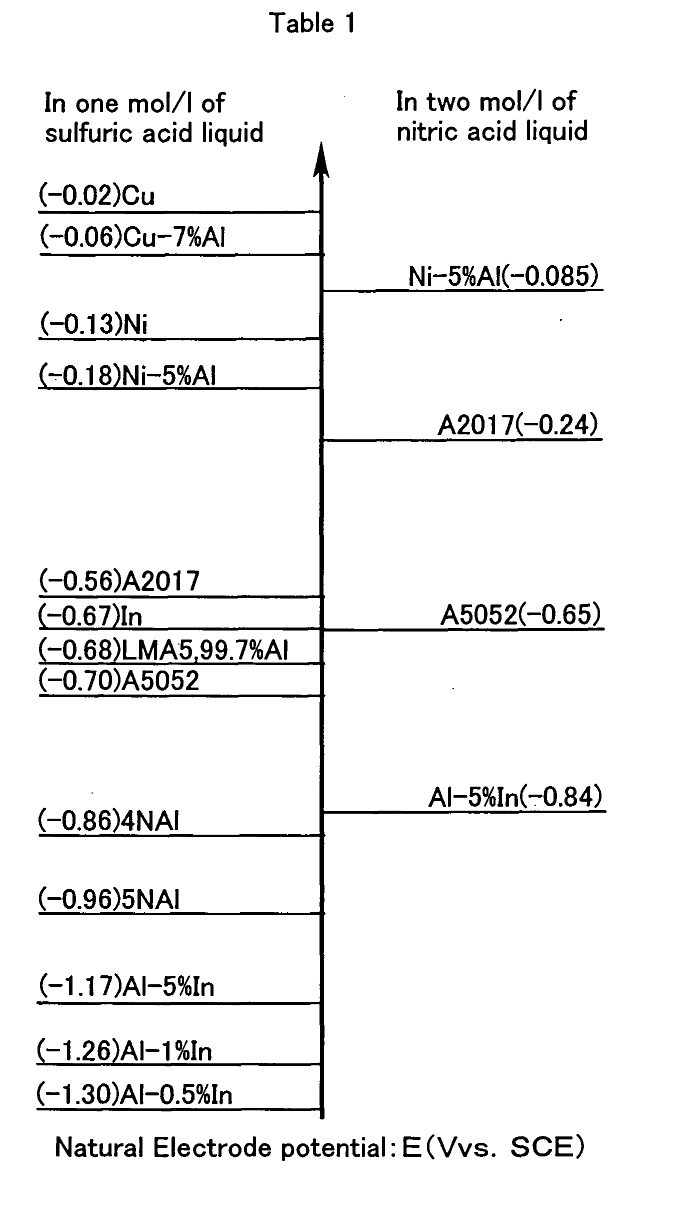
- a preferred material for forming the aforementioned lower readily-soluble metal film layer is a metal more readily soluble to the cleaning fluid S than the matrix metal material 1, for example, a copper alloy. If the matrix metal material 1 is or an aluminum alloy, the natural potential electrode measurement data show that copper alloy (JIS A5052 is -1.02 in one mol/l of sulfuric acid liquid) is more noble than or an alloy of aluminum (JIS A5052 is -1.70 in one mol/l of sulfuric acid liquid), as shown in Table 1.
- a local cell may be formed between or an alloy of aluminum and or an alloy of copper from the potential difference therebetween to promote the oxidization so that the matrix metal material 1 will more be dissolved.
- a more noble metal is one located above the reference metal in the table 1 while a less noble metal is one located below the reference metal in the table 1. Thus, whether a metal is more or less noble is determined relative to the reference metal.
- the present invention can separate the deposited film d from the matrix metal material 1 along with the metal film layer 2 for a shortened time period (e.g., about 45 minutes) by forming a metal film layer 2 containing a metal less noble than the matrix metal material 1 on the surface of the matrix metal material 1 through thermal spraying, vapor depositing, sputtering, laminate or other process and by causing a local cell to be formed between the matrix metal material 1 and the metal film layer 2 to promote the dissolution of the metal film layer 2 when the matrix metal material 1 is dipped in the cleaning fluid S.
- a shortened time period e.g., about 45 minutes
- the local cell is formed between the matrix metal material 1 and metal film layer 2 by the potential difference therebetween, the local current then flowing from the matrix metal material 1 to the metal film layer 2.
- the metal film layer preferentially dissolves and remains in the cleaning fluid as metal ions.
- the metal film layer 2 is Al -5% In (its natural potential is -1.17 in one mol/l of sulfuric acid liquid) and the matrix metal material 1 is Al alloy (the natural electrode potential of JIS A5052 is -0.70 in one mol/l of sulfuric acid liquid) and when the deposited film d of 99.99%Al (4N-Al) (its natural potential is - 0.86 in one mol/l of sulfuric acid liquid) deposits over the metal film layer 2, a local cell is formed between the matrix metal material 1 and the metal film layer 2 in the sulfuric acid liquid.
- the metal film layer 2 is ionized and dissolved into the sulfuric acid liquid.
- the metal film layer 2 may suitably be selected from a group consisting of metals and alloys that can easily form the local cell between the metal film layer 2 and the matrix metal material 1, based on the natural potential E (Vvs.SCE) in the cleaning fluid S.
- a second metal film layer 3 formed on the surface of the aforementioned metal film layer 2 through thermal spraying, vapor depositing, sputtering, laminating or other process, the second metal film layer 3 containing a metal more noble than the matrix metal material 1.
- the metal film layer 2 is Al-5%In
- the second metal film layer 3 is Al alloy (the natural potential of JIS A2017 is -0.56 in one mol/l of sulfuric acid liquid)
- the matrix metal material 1 is Al alloy (JIS A5052) and when 99.99%Al (4N-Al) film deposits on the second metal film layer 3, local cells are formed between the matrix metal material 1 and the metal film layer 2 and between the second metal film layer 3 and the metal film layer 2, respectively, in the sulfuric acid liquid.
- the metal film layer 2 is ionized and dissolved into the sulfuric acid liquid.
- time required to dissolve the metal film layer 2 and separate the deposited film d from the matrix metal material 1 was about 15 minutes.
- reference numeral 4 denotes a power source for applying a positive electric field to the matrix metal material 1 so that it will function as anode.
- the negative side of the power source 4 is connected to a cathode 5.
- the matrix metal material 1 may be less noble than the deposited film d or the second metal film layer 3. In this case, the matrix metal material 1 may dissolve into the cleaning fluid S.
- the present invention can separate the deposited film d from the matrix metal material 1 for an extremely shortened time period, without damaging the matrix metal material 1 itself from the cleaning fluid S by providing the aforementioned metal film layer 2 on the surface of the matrix metal material 1 of the component to form the local cell between the metal film layer 2 and the matrix metal material 1 or by providing the second metal film layer 3 on the surface of metal film layer 2 to form the local cell between the metal film layer 2 and the second metal film layer 3.
- it can be promoted to reuse the component while the life thereof can be extended.
- the present invention provides the component for the film forming equipments and the method of cleaning the same are suitable for use in formation of the thin film on the substrate such as buffer plate (e.g., substrate mask) or wafer support plate from the film forming material through vapor depositing, sputtering, CVD or other process since the deposited film can be separated from the film forming equipment component for a shortened time period so that the matrix metal material can be less damaged by the cleaning fluid and since the components of the present invention and method thereof are led to extend the life of the components, reduce the running cost for the film forming equipment, and save the resource.
- buffer plate e.g., substrate mask
- wafer support plate e.g., wafer support plate from the film forming material through vapor depositing, sputtering, CVD or other process since the deposited film can be separated from the film forming equipment component for a shortened time period so that the matrix metal material can be less damaged by the cleaning fluid and since the components of the present invention and method thereof are led to extend the life of the components
Landscapes
- Chemical & Material Sciences (AREA)
- Organic Chemistry (AREA)
- Engineering & Computer Science (AREA)
- Materials Engineering (AREA)
- Metallurgy (AREA)
- Mechanical Engineering (AREA)
- Chemical Kinetics & Catalysis (AREA)
- General Chemical & Material Sciences (AREA)
- Electrochemistry (AREA)
- Physical Vapour Deposition (AREA)
- Cleaning And De-Greasing Of Metallic Materials By Chemical Methods (AREA)
- Laminated Bodies (AREA)
- Other Surface Treatments For Metallic Materials (AREA)
- Coating By Spraying Or Casting (AREA)
- Cleaning By Liquid Or Steam (AREA)
Abstract
Description
Claims (4)
- A component for a film forming equipment forming a thin film on a substrate, the component being characterized by that a metal film layer electrochemically less noble than the matrix metal material of said component is formed on the surface of the matrix metal material through thermal spraying, vapor depositing, sputtering, laminating or other process.
- The component as claimed in claim 1, characterized by that a second metal film layer electrochemically more noble than said matrix metal material is formed on the surface of said metal film layer through thermal spraying, vapor depositing, sputtering, laminating or other process.
- A method of cleaning a component for a film forming equipment, characterized by that after a thin film has been formed on the substrate by the film forming equipment, the component as claimed in claim 1 or 2 is dipped in a cleaning fluid to remove an deposited film consisting of the film forming material from the component.
- The method as claimed in claim 3, characterized by that a positive electric field is applied to the matrix metal material of said component dipped in the cleaning fluid.
Applications Claiming Priority (3)
| Application Number | Priority Date | Filing Date | Title |
|---|---|---|---|
| JP2003040837 | 2003-02-19 | ||
| JP2003040837 | 2003-02-19 | ||
| PCT/JP2004/001799 WO2004074545A1 (en) | 2003-02-19 | 2004-02-18 | Film-forming apparatus component and method for cleaning same |
Publications (2)
| Publication Number | Publication Date |
|---|---|
| EP1595976A1 true EP1595976A1 (en) | 2005-11-16 |
| EP1595976A4 EP1595976A4 (en) | 2011-05-04 |
Family
ID=32905268
Family Applications (1)
| Application Number | Title | Priority Date | Filing Date |
|---|---|---|---|
| EP04712191A Withdrawn EP1595976A4 (en) | 2003-02-19 | 2004-02-18 | FILM COMPONENT COMPONENT AND METHOD OF CLEANING THE SAME |
Country Status (9)
| Country | Link |
|---|---|
| US (1) | US8216654B2 (en) |
| EP (1) | EP1595976A4 (en) |
| JP (1) | JP4436802B2 (en) |
| KR (1) | KR101024045B1 (en) |
| CN (1) | CN100476037C (en) |
| CA (1) | CA2511833C (en) |
| MY (1) | MY142434A (en) |
| TW (1) | TW200500479A (en) |
| WO (1) | WO2004074545A1 (en) |
Families Citing this family (6)
| Publication number | Priority date | Publication date | Assignee | Title |
|---|---|---|---|---|
| CN103240484A (en) * | 2012-02-01 | 2013-08-14 | 上海科秉电子科技有限公司 | Method for roughening inner layer surface of U-shaped groove |
| CN104614933A (en) * | 2014-12-24 | 2015-05-13 | 信利(惠州)智能显示有限公司 | A cleaning method of a metal film forming mask |
| KR102454433B1 (en) * | 2015-05-28 | 2022-10-17 | 삼성디스플레이 주식회사 | Apparatus of forming a film and cleaning method thereof |
| CN107946164B (en) * | 2017-11-20 | 2019-09-27 | 深圳市华星光电技术有限公司 | One kind preventing plate and its preparation method and application |
| CN108611599B (en) * | 2018-08-01 | 2020-08-21 | 京东方科技集团股份有限公司 | Method and device for cleaning mask |
| CN109576648A (en) * | 2018-12-29 | 2019-04-05 | 福建华佳彩有限公司 | One kind preventing plate |
Family Cites Families (22)
| Publication number | Priority date | Publication date | Assignee | Title |
|---|---|---|---|---|
| JPS52136818A (en) * | 1976-05-13 | 1977-11-15 | Daido Metal Co Ltd | Bearing metal for large size engine |
| GB2040315B (en) * | 1978-12-13 | 1983-05-11 | Glyco Metall Werke | Laminar material or element and a process for its manufacture |
| JPS55130817A (en) * | 1979-03-29 | 1980-10-11 | Matsushita Electric Ind Co Ltd | Producing boron structural material |
| JPS62109971A (en) | 1985-11-08 | 1987-05-21 | Matsushita Electronics Corp | Method for removing deposit in vacuum deposition vessel |
| JPS62287063A (en) | 1986-06-03 | 1987-12-12 | Fujitsu Ltd | Method for removing matter sticking to thin film treating equipment |
| JPH02259064A (en) | 1989-03-31 | 1990-10-19 | Pentel Kk | How to remove attached film from vacuum thin film forming equipment |
| JPH0387357A (en) | 1989-06-13 | 1991-04-12 | Nippon Mining Co Ltd | Thin film forming device |
| JPH04198500A (en) | 1990-11-28 | 1992-07-17 | Neos Co Ltd | Washing of metal base body |
| JPH05179424A (en) | 1991-12-26 | 1993-07-20 | Nisshin Steel Co Ltd | Steel sheet plated with different metals on front and rear sides |
| JPH05206098A (en) | 1992-01-28 | 1993-08-13 | Hitachi Metals Ltd | Method for etching ceramic substrate having metal multilayer film |
| JPH05230624A (en) * | 1992-02-20 | 1993-09-07 | Fujitsu Ltd | Method for preventing generation of dust in internal jig of pvd device and internal jig treating apparatus |
| JPH0649626A (en) | 1992-04-21 | 1994-02-22 | Ulvac Japan Ltd | Parts for film forming device and reproduction method therefor |
| JPH06220600A (en) * | 1993-01-21 | 1994-08-09 | Neos Co Ltd | Washing method of vacuum thin film forming device or the like |
| JPH06346254A (en) | 1993-06-14 | 1994-12-20 | Nisshin Steel Co Ltd | High corrosion resistance Zn / Cr multi-layer plated steel sheet and manufacturing method |
| JPH0783133A (en) | 1993-09-17 | 1995-03-28 | Kubota Corp | Spark ignition multi-cylinder engine |
| US5626943A (en) * | 1994-06-02 | 1997-05-06 | The Carborundum Company | Ultra-smooth ceramic substrates and magnetic data storage media prepared therefrom |
| JPH08165582A (en) * | 1994-12-13 | 1996-06-25 | Sumitomo Electric Ind Ltd | Terminal material |
| US5895696A (en) * | 1996-07-01 | 1999-04-20 | Alyn Corporation | Metal-clad ceramic-metal matrix composites for magnetic disk substrates for hard disk drives |
| JP3534989B2 (en) * | 1997-10-16 | 2004-06-07 | 株式会社アルバック | Component parts for film forming equipment |
| JP2000311879A (en) * | 1999-04-28 | 2000-11-07 | Mitsubishi Electric Corp | Cleaning liquid and method for manufacturing semiconductor device using the same |
| JP2002030494A (en) | 2000-07-13 | 2002-01-31 | Sumitomo Electric Ind Ltd | Corrosion resistant conductive material |
| US6899798B2 (en) * | 2001-12-21 | 2005-05-31 | Applied Materials, Inc. | Reusable ceramic-comprising component which includes a scrificial surface layer |
-
2004
- 2004-02-18 KR KR1020057010901A patent/KR101024045B1/en not_active Expired - Lifetime
- 2004-02-18 JP JP2005502737A patent/JP4436802B2/en not_active Expired - Lifetime
- 2004-02-18 CN CNB2004800023525A patent/CN100476037C/en not_active Expired - Lifetime
- 2004-02-18 CA CA2511833A patent/CA2511833C/en not_active Expired - Lifetime
- 2004-02-18 US US10/538,856 patent/US8216654B2/en not_active Expired - Lifetime
- 2004-02-18 WO PCT/JP2004/001799 patent/WO2004074545A1/en not_active Ceased
- 2004-02-18 EP EP04712191A patent/EP1595976A4/en not_active Withdrawn
- 2004-02-19 MY MYPI20040545A patent/MY142434A/en unknown
- 2004-02-19 TW TW093104120A patent/TW200500479A/en not_active IP Right Cessation
Also Published As
| Publication number | Publication date |
|---|---|
| MY142434A (en) | 2010-11-30 |
| KR20050109457A (en) | 2005-11-21 |
| US8216654B2 (en) | 2012-07-10 |
| CA2511833A1 (en) | 2004-09-02 |
| KR101024045B1 (en) | 2011-03-22 |
| CN1738926A (en) | 2006-02-22 |
| CA2511833C (en) | 2012-03-20 |
| EP1595976A4 (en) | 2011-05-04 |
| CN100476037C (en) | 2009-04-08 |
| JP4436802B2 (en) | 2010-03-24 |
| TW200500479A (en) | 2005-01-01 |
| WO2004074545A1 (en) | 2004-09-02 |
| US20060246735A1 (en) | 2006-11-02 |
| TWI315350B (en) | 2009-10-01 |
| JPWO2004074545A1 (en) | 2006-06-01 |
Similar Documents
| Publication | Publication Date | Title |
|---|---|---|
| JP5770575B2 (en) | Formation method of oxide film | |
| JP2009068071A (en) | Protective plate, vacuum processing apparatus, and method of regenerating proof plate | |
| US8216654B2 (en) | Components for a film-forming device and method for cleaning the same | |
| TW570993B (en) | Sputtering target producing very few particles, backing plate or apparatus within sputtering device and roughening method by electric discharge machining | |
| JP4653406B2 (en) | Water-disintegrating Al composite material, water-disintegrating Al sprayed film, method for producing water-disintegrating Al powder, film forming chamber component, and method for recovering film forming material | |
| KR20210000668A (en) | Surface treatment method | |
| JPH05230628A (en) | Metal film forming apparatus, metal material recovery method in metal film forming apparatus | |
| US10156018B2 (en) | Method for manufacturing anodic metal oxide nanoporous templates | |
| CN102027152A (en) | Water-reactive Al composite material, water-reactive Al film, process for production of the Al film, and constituent member for film deposition chamber | |
| RU2468117C2 (en) | Al COMPOSITE MATERIAL REACTING WITH WATER, Al FILM REACTING WITH WATER, METHOD TO PRODUCE THIS Al FILM AND COMPONENT OF FILM-PRODUCING CHAMBER | |
| CN106191793B (en) | Film forming apparatus and cleaning method thereof | |
| JP3534989B2 (en) | Component parts for film forming equipment | |
| Ley | Wafer-scale controlled spalling and reuse of (100)-oriented germanium | |
| EP1586673B1 (en) | Component for film forming device and method of washing the component | |
| JP2002093719A (en) | Metal material member for film forming apparatus and film forming apparatus using the same | |
| WO2019073819A1 (en) | Method of peeling adhesion metal from metal plate | |
| JP2949615B2 (en) | How to remove the adhered film | |
| JPH1060621A (en) | How to remove the adhered film | |
| TWI228157B (en) | ECP method and apparatus thereof | |
| KR20180131279A (en) | Method of recycling aluminum member | |
| JP2626823B2 (en) | Thin film forming equipment | |
| JP2004315948A (en) | Contamination prevention device for thin film deposition system | |
| JPH08277469A (en) | Wafer clamp device recycling method | |
| JPH10259471A (en) | Jig for vapor deposition and method for recovering noble metal from jig for vapor deposition | |
| JP2005017806A (en) | Multilayer optical element manufacturing method |
Legal Events
| Date | Code | Title | Description |
|---|---|---|---|
| PUAI | Public reference made under article 153(3) epc to a published international application that has entered the european phase |
Free format text: ORIGINAL CODE: 0009012 |
|
| 17P | Request for examination filed |
Effective date: 20050614 |
|
| AK | Designated contracting states |
Kind code of ref document: A1 Designated state(s): AT BE BG CH CY CZ DE DK EE ES FI FR GB GR HU IE IT LI LU MC NL PT RO SE SI SK TR |
|
| AX | Request for extension of the european patent |
Extension state: AL LT LV MK |
|
| DAX | Request for extension of the european patent (deleted) | ||
| RBV | Designated contracting states (corrected) |
Designated state(s): DE FR GB |
|
| A4 | Supplementary search report drawn up and despatched |
Effective date: 20110406 |
|
| RIC1 | Information provided on ipc code assigned before grant |
Ipc: C23C 14/56 20060101ALI20110331BHEP Ipc: H01L 21/205 20060101ALI20110331BHEP Ipc: C23F 1/00 20060101ALI20110331BHEP Ipc: C23C 16/44 20060101ALI20110331BHEP Ipc: C23C 14/00 20060101ALI20110331BHEP Ipc: C23C 30/00 20060101AFI20040906BHEP |
|
| 17Q | First examination report despatched |
Effective date: 20120125 |
|
| STAA | Information on the status of an ep patent application or granted ep patent |
Free format text: STATUS: THE APPLICATION IS DEEMED TO BE WITHDRAWN |
|
| 18D | Application deemed to be withdrawn |
Effective date: 20150303 |