EP1593154B1 - Method of manufacturing a semiconductor device with mos transistors comprising gate electrodes formed in a packet of metal layers deposited upon one another - Google Patents
Method of manufacturing a semiconductor device with mos transistors comprising gate electrodes formed in a packet of metal layers deposited upon one another Download PDFInfo
- Publication number
- EP1593154B1 EP1593154B1 EP04702397A EP04702397A EP1593154B1 EP 1593154 B1 EP1593154 B1 EP 1593154B1 EP 04702397 A EP04702397 A EP 04702397A EP 04702397 A EP04702397 A EP 04702397A EP 1593154 B1 EP1593154 B1 EP 1593154B1
- Authority
- EP
- European Patent Office
- Prior art keywords
- layer
- metal
- nitrogen
- deposited
- active regions
- Prior art date
- Legal status (The legal status is an assumption and is not a legal conclusion. Google has not performed a legal analysis and makes no representation as to the accuracy of the status listed.)
- Expired - Lifetime
Links
Images

Classifications
-
- H—ELECTRICITY
- H10—SEMICONDUCTOR DEVICES; ELECTRIC SOLID-STATE DEVICES NOT OTHERWISE PROVIDED FOR
- H10P—GENERIC PROCESSES OR APPARATUS FOR THE MANUFACTURE OR TREATMENT OF DEVICES COVERED BY CLASS H10
- H10P10/00—Bonding of wafers, substrates or parts of devices
-
- H—ELECTRICITY
- H10—SEMICONDUCTOR DEVICES; ELECTRIC SOLID-STATE DEVICES NOT OTHERWISE PROVIDED FOR
- H10P—GENERIC PROCESSES OR APPARATUS FOR THE MANUFACTURE OR TREATMENT OF DEVICES COVERED BY CLASS H10
- H10P95/00—Generic processes or apparatus for manufacture or treatments not covered by the other groups of this subclass
-
- H—ELECTRICITY
- H10—SEMICONDUCTOR DEVICES; ELECTRIC SOLID-STATE DEVICES NOT OTHERWISE PROVIDED FOR
- H10D—INORGANIC ELECTRIC SEMICONDUCTOR DEVICES
- H10D64/00—Electrodes of devices having potential barriers
- H10D64/01—Manufacture or treatment
- H10D64/013—Manufacture or treatment of electrodes having a conductor capacitively coupled to a semiconductor by an insulator
- H10D64/01302—Manufacture or treatment of electrodes having a conductor capacitively coupled to a semiconductor by an insulator the insulator being formed after the semiconductor body, the semiconductor being silicon
- H10D64/01304—Manufacture or treatment of electrodes having a conductor capacitively coupled to a semiconductor by an insulator the insulator being formed after the semiconductor body, the semiconductor being silicon characterised by the conductor
- H10D64/01316—Manufacture or treatment of electrodes having a conductor capacitively coupled to a semiconductor by an insulator the insulator being formed after the semiconductor body, the semiconductor being silicon characterised by the conductor the conductor comprising a layer of elemental metal contacting the insulator, e.g. Ta, W, Mo or Al
-
- H—ELECTRICITY
- H10—SEMICONDUCTOR DEVICES; ELECTRIC SOLID-STATE DEVICES NOT OTHERWISE PROVIDED FOR
- H10D—INORGANIC ELECTRIC SEMICONDUCTOR DEVICES
- H10D64/00—Electrodes of devices having potential barriers
- H10D64/01—Manufacture or treatment
- H10D64/013—Manufacture or treatment of electrodes having a conductor capacitively coupled to a semiconductor by an insulator
- H10D64/01302—Manufacture or treatment of electrodes having a conductor capacitively coupled to a semiconductor by an insulator the insulator being formed after the semiconductor body, the semiconductor being silicon
- H10D64/01304—Manufacture or treatment of electrodes having a conductor capacitively coupled to a semiconductor by an insulator the insulator being formed after the semiconductor body, the semiconductor being silicon characterised by the conductor
- H10D64/01318—Manufacture or treatment of electrodes having a conductor capacitively coupled to a semiconductor by an insulator the insulator being formed after the semiconductor body, the semiconductor being silicon characterised by the conductor the conductor comprising a layer of alloy material, compound material or organic material contacting the insulator, e.g. TiN
-
- H—ELECTRICITY
- H10—SEMICONDUCTOR DEVICES; ELECTRIC SOLID-STATE DEVICES NOT OTHERWISE PROVIDED FOR
- H10D—INORGANIC ELECTRIC SEMICONDUCTOR DEVICES
- H10D64/00—Electrodes of devices having potential barriers
- H10D64/60—Electrodes characterised by their materials
- H10D64/66—Electrodes having a conductor capacitively coupled to a semiconductor by an insulator, e.g. MIS electrodes
- H10D64/665—Electrodes having a conductor capacitively coupled to a semiconductor by an insulator, e.g. MIS electrodes the conductor comprising a layer of elemental metal contacting the insulator, e.g. tungsten or molybdenum
- H10D64/666—Electrodes having a conductor capacitively coupled to a semiconductor by an insulator, e.g. MIS electrodes the conductor comprising a layer of elemental metal contacting the insulator, e.g. tungsten or molybdenum the conductor further comprising additional layers
-
- H—ELECTRICITY
- H10—SEMICONDUCTOR DEVICES; ELECTRIC SOLID-STATE DEVICES NOT OTHERWISE PROVIDED FOR
- H10D—INORGANIC ELECTRIC SEMICONDUCTOR DEVICES
- H10D64/00—Electrodes of devices having potential barriers
- H10D64/60—Electrodes characterised by their materials
- H10D64/66—Electrodes having a conductor capacitively coupled to a semiconductor by an insulator, e.g. MIS electrodes
- H10D64/667—Electrodes having a conductor capacitively coupled to a semiconductor by an insulator, e.g. MIS electrodes the conductor comprising a layer of alloy material, compound material or organic material contacting the insulator, e.g. TiN workfunction layers
-
- H—ELECTRICITY
- H10—SEMICONDUCTOR DEVICES; ELECTRIC SOLID-STATE DEVICES NOT OTHERWISE PROVIDED FOR
- H10D—INORGANIC ELECTRIC SEMICONDUCTOR DEVICES
- H10D84/00—Integrated devices formed in or on semiconductor substrates that comprise only semiconducting layers, e.g. on Si wafers or on GaAs-on-Si wafers
- H10D84/01—Manufacture or treatment
- H10D84/0123—Integrating together multiple components covered by H10D12/00 or H10D30/00, e.g. integrating multiple IGBTs
- H10D84/0126—Integrating together multiple components covered by H10D12/00 or H10D30/00, e.g. integrating multiple IGBTs the components including insulated gates, e.g. IGFETs
- H10D84/0135—Manufacturing their gate conductors
- H10D84/014—Manufacturing their gate conductors the gate conductors having different materials or different implants
-
- H—ELECTRICITY
- H10—SEMICONDUCTOR DEVICES; ELECTRIC SOLID-STATE DEVICES NOT OTHERWISE PROVIDED FOR
- H10D—INORGANIC ELECTRIC SEMICONDUCTOR DEVICES
- H10D84/00—Integrated devices formed in or on semiconductor substrates that comprise only semiconducting layers, e.g. on Si wafers or on GaAs-on-Si wafers
- H10D84/01—Manufacture or treatment
- H10D84/02—Manufacture or treatment characterised by using material-based technologies
- H10D84/03—Manufacture or treatment characterised by using material-based technologies using Group IV technology, e.g. silicon technology or silicon-carbide [SiC] technology
- H10D84/038—Manufacture or treatment characterised by using material-based technologies using Group IV technology, e.g. silicon technology or silicon-carbide [SiC] technology using silicon technology, e.g. SiGe
Definitions
- the invention relates to a method of manufacturing a semiconductor device with MOS transistors comprising gate electrodes formed in a packet of metal layers deposited upon one another, in which method, on a surface of a silicon body on which border active regions of silicon and field isolation regions insulating these regions with respect to each other, a layer of a gate dielectric is formed at the location of the active regions, after which a layer of a first metal is deposited wherein nitrogen is introduced at the location of a part of the active regions, after which a layer of a second metal is deposited on the layer of the first metal, and subsequently the gate electrodes are etched in the packet of superposed metal layers.
- metal as used herein is to be taken to mean also conductive compounds of metals, such as for example metal silicides and metal nitrides.
- the MOS transistors whose gate electrodes are formed in the layer of the first metal into which nitrogen is introduced thus exhibit a different threshold voltage than the MOS transistors whose gate electrodes are formed in the layer of the first metal into which no nitrogen is introduced. It is thus possible to manufacture a semiconductor device with MOS transistors that exhibit a different threshold voltage.
- the part of the active regions where nitrogen is introduced into the layer of the first metal, and the other active regions are then provided with a p-type or n-type doping in a corresponding manner.
- the introduction of nitrogen may lead to so large an increase of the work function that NMOS and PMOS transistors can be manufactured which, in absolute terms, have an equal threshold voltage.
- the part of the active regions where nitrogen is introduced into the layer of the first metal is, for example, n-type doped, and the other active regions are p-type doped.
- the layer of the second metal is provided in a comparatively large thickness, as a result of which the gate electrodes formed in the two layers exhibit a comparatively low electric resistance; in the gate electrodes, the layer of the first metal is "shunted" by the layer of the second metal,
- US 6,451,690 describes a method of forming electrode structure and method of fabricating a semiconductor device. After forming a barrier film on a silicon-containing film including silicon as a main component, a high-melting-point metal film is deposited on the barrier film, so as to form a laminated structure including the silicon-containing film, the barrier film and the high-melting-point metal film. The laminated structure is subjected to a heat treatment at a temperature of 750 DEG C. or more.
- the barrier film is formed by forming a first film of a nitride of a metal on the film; forming, on the first metal film, a second metal film of the metal or the nitride of the metal with a smaller nitrogen content than the first metal film; and forming, on the second metal film, a third metal film of the nitride of the metal with a larger nitrogen content than the second metal film.
- US 2002/058374 describes a method of forming dual-metal gates in semiconductor devices.
- US 2001/0015463 A1 describes a method of the type mentioned in the opening paragraph, in which an approximately 100 nm thick layer of titanium is deposited as the layer of the first metal. Nitrogen ions are locally implanted in this layer to change the work function. An approximately 200 nm thick layer of tungsten is deposited as the layer of the second material. On the layer of tungsten, an etch mask of silicon nitride is formed, after which the gate electrodes are etched in the packet of superposed layers of tungsten and titanium nitride.
- titanium is used as the metal for the gate electrodes, a maximum change, in this case an increase, of the work function is obtained if the layer of titanium, upon the introduction of nitrogen, is completely converted to a layer of titanium nitride.
- the use of a thinner layer, so that converting this layer of titanium entirely to a layer of titanium nitride would require less nitrogen is impossible in practice because, during the ion implantation, the underlying gate dielectric could be damaged.
- an embodiment of the invention can obviate said drawbacks.
- an auxiliary layer of a third, nitrogen-permeable metal is formed on this layer.
- the layer of the first metal can be applied in a very small thickness of less than 10 nm, as a result of which, for example, the complete conversion of a layer of titanium to a layer of titanium nitride requires much less, i.e. a factor of 10, nitrogen than in the case of the known method described above.
- the energy with which the ion implantation can be carried out is such that practically all nitrogen ions are introduced into the auxiliary layer, so that the gate dielectric lying under the layer is not damaged.
- the nitrogen ions introduced into the auxiliary layer diffuse during a thermal treatment, which is customary in practice after an ion implantation, to the underlying layer of the first metal.
- the auxiliary layer may be removed.
- a simpler procedure is obtained, however, if, after nitrogen has been locally introduced into the layer of the first metal, the layer of the second metal is deposited on the auxiliary layer.
- the auxiliary layer can be advantageously used as an etch-stop layer during etching the layer of the second metal.
- the relatively thick layer of the second metal having a thickness of for example 200 nm
- the much thinner layer of the first metal having a thickness of for example approximately 10 nm
- the underlying layer of gate dielectric are protected by the auxiliary layer.
- the risk of damage to the layer of the first metal and the underlying gate dielectric is much smaller if the nitrogen is introduced into the layer of the first metal by diffusion from a layer of a solid substance containing an excess of nitrogen which is provided on the auxiliary layer at the location of the active regions of the first conductivity type. After nitrogen has been introduced into the layer of the first metal, said solid nitrogen source can be removed using the auxiliary layer as an etch stop.
- a substantially complete conversion of the first metal to a metal nitride can be achieved if a layer of TiN x , where x > 1, is provided on the auxiliary layer as a layer of a solid substance containing an excess of nitrogen. During the subsequent thermal treatment, nitrogen diffuses in atomic form through the auxiliary layer into the layer of the first metal, as a result of which a chemical reaction with the first metal can take place efficiently.
- the first metal of which a layer is deposited on the layer of gate dielectric
- use can be made of many metals, such as tantalum, molybdenum, zirconium, hafnium, vanadium and niobium, and metal silicides.
- the auxiliary layer use can be made of many metals.
- a layer of tantalum or molybdenum is deposited whose work function without nitrogen is 4.15 eV and 4.5 eV, respectively, and, after nitridation, 5.4 eV and 5.3 eV, respectively.
- auxiliary layer use is preferably made of a layer of cobalt or nickel, which metals are properly nitrogen-permeable and form an excellent etch stop when etching a layer of tungsten in a fluor-containing plasma that is deposited on said auxiliary layer.
- This enables substantial changes in work function to be achieved, and cobalt and nickel readily pass nitrogen, which is important in particular when use is made of a solid nitrogen source, while these layers are also very suitable as an etch stop when etch-patterning the layer of the second metal, which second metal may also be chosen from a large number of suitable metals, such as inter alia tungsten, which is very suitable.
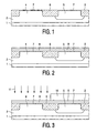
- Figs. 1 through 6 are diagrammatic, cross-sectional views of several stages in the manufacture of a semiconductor device with PMOS and NMOS transistors comprising gate electrodes formed in a packet of metal layers deposited upon one another.
- a silicon body 1 with a customary, epitaxially grown n-type top layer 2 and a surface 3 on which border active regions 4 of a first conductivity type, in this example n-type, and active regions 5 of the second conductivity type, in this example p-type.
- the n-type active regions 4 form part of the epitaxially grown layer 2, the p-type active regions are formed therein by ion implantation.
- the active regions 4 and 5 are insulated with respect to each other by field isolation regions 6 which also border on the surface 3.
- the PMOS transistors are formed, and at the location of the active regions 5, the NMOS transistors are formed.
- the method can also suitably be used to manufacture a semiconductor device with MOS transistors of the same type (N or P) which have a different threshold voltage.
- MOS transistors of the same type N or P
- nitrogen is then introduced into the layer of the first metal, so that the transistors at said locations obtain a threshold voltage that is different from that of the transistors formed at the location of the other active regions.
- all active regions are p-type or n-type doped in the same manner.
- an approximately 5 nm thick layer of a gate dielectric 7 is formed at the location of the p-type active regions 4 and the n-type active regions 5. This can be achieved by thermal oxidation of silicon that borders on the surface 3, but also by deposition of a layer of a suitable material. If the layer is deposited, not only silicon oxide but also, for example, silicon oxynitride or aluminum oxide can be used as the gate dielectric.
- a layer 8 of a first metal in this example an approximately 10 nm thick layer of tantalum or molybdenum, is deposited on the structure shown in Fig. 1 .
- Nitrogen is introduced into this layer at the location of a part of the active regions, in this example at the location of the n-type active regions 4.
- the first metal obtains a higher work function at said locations. It can thus be achieved that the work function of the first metal 8 at the location of the n-type active regions 4 becomes so much higher than that of the first metal 8 at the location of the p-type active regions 5, that, measured in absolute terms, the threshold voltage of the PMOS and NMOS transistors to be formed is equal,.
- the nitrogen is introduced into the layer of the first metal 8 by means of ion implantation.
- a customary photoresist mask 10 is provided on the auxiliary layer 9, which mask covers the layer of the first metal at the location of the p-type active regions 5 and leaves said layer exposed at the location of the n-type regions 4.
- nitrogen ions are introduced into the layer of the first metal 8, as diagrammatically indicated in Fig. 3 by means of arrows 11.
- the photoresist mask 10 is removed.
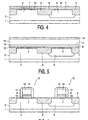
- the layer of the first metal 8 is preferably converted to a layer 12 of a nitride of the first metal; the greatest possible increase of the work function of the first metal is thus achieved.
- the layer of the first metal 8 has, in this case, a thickness of only 10 nm.
- the layer 8 can be completely converted to a layer 12 of metal nitride by means of a comparatively small quantity of nitrogen. What is required for this is a dose of approximately 5.10 16 nitrogen ions per cm 2 .
- the ion implantation can be carried out with such energy, in this case 0.5 keV, that practically all the nitrogen ions are introduced into the auxiliary layer 9, so that the gate dielectric 7 situated underneath the layer of the first metal 8 is not damaged.
- the nitrogen ions introduced into the auxiliary layer 9 diffuse during a thermal treatment, carried out after the implantation process, to the underlying layer of the first metal.
- the silicon body 1 is heated at a temperature of approximately 800 °C for approximately 30 seconds.
- the gate electrodes 15 for the NMOS transistors are formed in the layer packet 8, 9, 13, 14 thus formed, as shown in Fig. 6
- the gate electrodes 16 for the PMOS transistors are formed in the layer packet 12, 9, 13, 14 thus formed.
- the layers of silicon nitride 14 and tungsten 13 are etched in a fluor-containing plasma formed in a gas mixture containing CF 4 and CHF 3 , after which the auxiliary layer of cobalt or nickel is removed by wet etching in an etch bath containing sulfuric acid and peroxide, whereafter the layer of the first metal 8, 12 is etched in said fluor-containing plasma.
- the gate electrodes are further provided with insulating spacers 17 in a customary manner.
- the layer of the second metal 13 is provided in a comparatively large thickness, as a result of which the gate electrodes 15, 16 forme exhibit a comparatively low electric resistance; in the gate electrodes, the layer of the first metal 8, 12 is "shunted" by the layer of the second metal 13.
- the auxiliary layer 9 is not removed, in this case.
- the auxiliary layer is used as an etch stop in the process of etching the layer of the second metal.
- the layer of the first metal 8, the layer of nitride of the first metal 12 and the underlying layer of the gate dielectric 7 are protected by the auxiliary layer 9.
- Figs. 7 and 8 diagrammatically show a different method of introducing nitrogen into the layer of the first metal 8.
- a layer 18 of a solid substance containing an excess of nitrogen is provided on the auxiliary layer 9, at the location of the n-type active regions 4.
- a layer of TiN x where x > 1, is provided as the layer of a solid substance 18 containing an excess of nitrogen. This is carried out, for example, in a customary sputtering apparatus wherein a target of titanium is sputtered by a plasma formed in a gas mixture with argon and an excess of nitrogen. From the layer 18 the nitrogen is introduced into the layer of the first metal 8 by diffusion of nitrogen through the auxiliary layer 9.
- the silicon body 1 is heated at a temperature of approximately 700 °C for approximately 30 seconds.
- nitrogen diffuses in atomic form through the auxiliary layer 9 into the layer of the first metal 12; as a result, the chemical reaction takes place very efficiently.
- the solid nitrogen source 17 is etched away in an etch bath with ammonia and peroxide.
- the auxiliary layer 9 of cobalt or nickel is used as an etch stop in this process.
- the manufacture of the transistors further proceeds as shown in Figs. 5 and 6 .
- the first metal of which a layer 8 is deposited on the layer of gate dielectric 7
- use can be made of many metals, such as tantalum, molybdenum, zirconium, hafnium, vanadium and niobium, as well as metal silicides.
- the auxiliary layer 9 use can be made of many metals.
- a layer of tantalum or molybdenum is deposited as a layer of the first metal 8, on which a layer of cobalt or nickel is deposited as the auxiliary layer 9.
Landscapes
- Metal-Oxide And Bipolar Metal-Oxide Semiconductor Integrated Circuits (AREA)
- Insulated Gate Type Field-Effect Transistor (AREA)
- Electrodes Of Semiconductors (AREA)
Abstract
Description
- The invention relates to a method of manufacturing a semiconductor device with MOS transistors comprising gate electrodes formed in a packet of metal layers deposited upon one another, in which method, on a surface of a silicon body on which border active regions of silicon and field isolation regions insulating these regions with respect to each other, a layer of a gate dielectric is formed at the location of the active regions, after which a layer of a first metal is deposited wherein nitrogen is introduced at the location of a part of the active regions, after which a layer of a second metal is deposited on the layer of the first metal, and subsequently the gate electrodes are etched in the packet of superposed metal layers.
- The term "metals" as used herein is to be taken to mean also conductive compounds of metals, such as for example metal silicides and metal nitrides. The layer of the first metal into which nitrogen is locally introduced, and which can thus be locally entirely converted to a metal nitride, consequently remains a layer of "metal".
- Into the layer of the first metal, which is formed on the layer of gate dielectric, nitrogen is introduced at the location of a part of the active regions, as a result of which the first metal obtains a different work function there. The MOS transistors whose gate electrodes are formed in the layer of the first metal into which nitrogen is introduced thus exhibit a different threshold voltage than the MOS transistors whose gate electrodes are formed in the layer of the first metal into which no nitrogen is introduced. It is thus possible to manufacture a semiconductor device with MOS transistors that exhibit a different threshold voltage. The part of the active regions where nitrogen is introduced into the layer of the first metal, and the other active regions are then provided with a p-type or n-type doping in a corresponding manner. For some metals, such as titanium, the introduction of nitrogen may lead to so large an increase of the work function that NMOS and PMOS transistors can be manufactured which, in absolute terms, have an equal threshold voltage. The part of the active regions where nitrogen is introduced into the layer of the first metal is, for example, n-type doped, and the other active regions are p-type doped.
- The layer of the second metal is provided in a comparatively large thickness, as a result of which the gate electrodes formed in the two layers exhibit a comparatively low electric resistance; in the gate electrodes, the layer of the first metal is "shunted" by the layer of the second metal,
-
US 6,451,690 describes a method of forming electrode structure and method of fabricating a semiconductor device. After forming a barrier film on a silicon-containing film including silicon as a main component, a high-melting-point metal film is deposited on the barrier film, so as to form a laminated structure including the silicon-containing film, the barrier film and the high-melting-point metal film. The laminated structure is subjected to a heat treatment at a temperature of 750 DEG C. or more. The barrier film is formed by forming a first film of a nitride of a metal on the film; forming, on the first metal film, a second metal film of the metal or the nitride of the metal with a smaller nitrogen content than the first metal film; and forming, on the second metal film, a third metal film of the nitride of the metal with a larger nitrogen content than the second metal film. -
US 2002/058374 describes a method of forming dual-metal gates in semiconductor devices. -
US 2001/0015463 A1 describes a method of the type mentioned in the opening paragraph, in which an approximately 100 nm thick layer of titanium is deposited as the layer of the first metal. Nitrogen ions are locally implanted in this layer to change the work function. An approximately 200 nm thick layer of tungsten is deposited as the layer of the second material. On the layer of tungsten, an etch mask of silicon nitride is formed, after which the gate electrodes are etched in the packet of superposed layers of tungsten and titanium nitride. - If titanium is used as the metal for the gate electrodes, a maximum change, in this case an increase, of the work function is obtained if the layer of titanium, upon the introduction of nitrogen, is completely converted to a layer of titanium nitride. This requires a very large quantity of nitrogen to be implanted, in a layer of titanium having a thickness of 100 nm more than 5. 1017 nitrogen atoms per cm2 must be implanted. In practice this requires an expensive process step which is also very time consuming. The use of a thinner layer, so that converting this layer of titanium entirely to a layer of titanium nitride would require less nitrogen is impossible in practice because, during the ion implantation, the underlying gate dielectric could be damaged.
- The invention is defined in the accompanying claims. An embodiment of the invention can obviate said drawbacks. According to an embodiment of the invention, before nitrogen is locally introduced into the layer of the first metal, an auxiliary layer of a third, nitrogen-permeable metal is formed on this layer. By virtue thereof, the layer of the first metal can be applied in a very small thickness of less than 10 nm, as a result of which, for example, the complete conversion of a layer of titanium to a layer of titanium nitride requires much less, i.e. a factor of 10, nitrogen than in the case of the known method described above. If the nitrogen is introduced into the layer of the first metal by means of ion implantation, then the energy with which the ion implantation can be carried out is such that practically all nitrogen ions are introduced into the auxiliary layer, so that the gate dielectric lying under the layer is not damaged. The nitrogen ions introduced into the auxiliary layer diffuse during a thermal treatment, which is customary in practice after an ion implantation, to the underlying layer of the first metal.
- After nitrogen has been introduced into the layer of the first metal, the auxiliary layer may be removed. A simpler procedure is obtained, however, if, after nitrogen has been locally introduced into the layer of the first metal, the layer of the second metal is deposited on the auxiliary layer. In this case, during etching the gate electrodes in the packet of the three metal layers, the auxiliary layer can be advantageously used as an etch-stop layer during etching the layer of the second metal. During etching the relatively thick layer of the second metal, having a thickness of for example 200 nm, the much thinner layer of the first metal, having a thickness of for example approximately 10 nm, and the underlying layer of gate dielectric are protected by the auxiliary layer.
- The risk of damage to the layer of the first metal and the underlying gate dielectric is much smaller if the nitrogen is introduced into the layer of the first metal by diffusion from a layer of a solid substance containing an excess of nitrogen which is provided on the auxiliary layer at the location of the active regions of the first conductivity type. After nitrogen has been introduced into the layer of the first metal, said solid nitrogen source can be removed using the auxiliary layer as an etch stop.
- A substantially complete conversion of the first metal to a metal nitride can be achieved if a layer of TiNx, where x > 1, is provided on the auxiliary layer as a layer of a solid substance containing an excess of nitrogen. During the subsequent thermal treatment, nitrogen diffuses in atomic form through the auxiliary layer into the layer of the first metal, as a result of which a chemical reaction with the first metal can take place efficiently.
- For the first metal, of which a layer is deposited on the layer of gate dielectric, use can be made of many metals, such as tantalum, molybdenum, zirconium, hafnium, vanadium and niobium, and metal silicides. Also for the auxiliary layer use can be made of many metals. Preferably, however, as the layer of the first metal, a layer of tantalum or molybdenum is deposited whose work function without nitrogen is 4.15 eV and 4.5 eV, respectively, and, after nitridation, 5.4 eV and 5.3 eV, respectively. For the auxiliary layer use is preferably made of a layer of cobalt or nickel, which metals are properly nitrogen-permeable and form an excellent etch stop when etching a layer of tungsten in a fluor-containing plasma that is deposited on said auxiliary layer. This enables substantial changes in work function to be achieved, and cobalt and nickel readily pass nitrogen, which is important in particular when use is made of a solid nitrogen source, while these layers are also very suitable as an etch stop when etch-patterning the layer of the second metal, which second metal may also be chosen from a large number of suitable metals, such as inter alia tungsten, which is very suitable.
- These and other aspects of the invention are apparent from and will be elucidated with reference to the embodiment(s) described hereinafter.
- In the drawings:
-
Figs. 1 through 6 are diagrammatic, cross-sectional views of several stages in the manufacture of a semiconductor device by means of a first embodiment of the method in accordance with the invention, and -
Figs. 7 and 8 are diagrammatic, cross-sectional views of several stages in the manufacture of a semiconductor device by means of a second embodiment of the method in accordance with the invention. -
Figs. 1 through 6 are diagrammatic, cross-sectional views of several stages in the manufacture of a semiconductor device with PMOS and NMOS transistors comprising gate electrodes formed in a packet of metal layers deposited upon one another. In this case, as shown inFig. 1 , as a basis use is made of asilicon body 1 with a customary, epitaxially grown n-type top layer 2 and asurface 3 on which borderactive regions 4 of a first conductivity type, in this example n-type, andactive regions 5 of the second conductivity type, in this example p-type. The n-typeactive regions 4 form part of the epitaxially grownlayer 2, the p-type active regions are formed therein by ion implantation. Theactive regions field isolation regions 6 which also border on thesurface 3. At the location of theactive regions 4, the PMOS transistors are formed, and at the location of theactive regions 5, the NMOS transistors are formed. - It is to be noted that the method can also suitably be used to manufacture a semiconductor device with MOS transistors of the same type (N or P) which have a different threshold voltage. At the location of a part of the active regions, nitrogen is then introduced into the layer of the first metal, so that the transistors at said locations obtain a threshold voltage that is different from that of the transistors formed at the location of the other active regions. In this case, all active regions are p-type or n-type doped in the same manner.
- As is also shown in
Fig. 1 , an approximately 5 nm thick layer of a gate dielectric 7 is formed at the location of the p-typeactive regions 4 and the n-typeactive regions 5. This can be achieved by thermal oxidation of silicon that borders on thesurface 3, but also by deposition of a layer of a suitable material. If the layer is deposited, not only silicon oxide but also, for example, silicon oxynitride or aluminum oxide can be used as the gate dielectric. - As shown in
Fig. 2 , alayer 8 of a first metal, in this example an approximately 10 nm thick layer of tantalum or molybdenum, is deposited on the structure shown inFig. 1 . Nitrogen is introduced into this layer at the location of a part of the active regions, in this example at the location of the n-typeactive regions 4. As a result, the first metal obtains a higher work function at said locations. It can thus be achieved that the work function of thefirst metal 8 at the location of the n-typeactive regions 4 becomes so much higher than that of thefirst metal 8 at the location of the p-typeactive regions 5, that, measured in absolute terms, the threshold voltage of the PMOS and NMOS transistors to be formed is equal,. - In the first exemplary embodiment of the method, the nitrogen is introduced into the layer of the
first metal 8 by means of ion implantation. First anauxiliary layer 9, in this example an approximately 10 nm thick layer of cobalt or nickel, is deposited on the layer of thefirst metal 8. Subsequently, as shown inFig. 3 , acustomary photoresist mask 10 is provided on theauxiliary layer 9, which mask covers the layer of the first metal at the location of the p-typeactive regions 5 and leaves said layer exposed at the location of the n-type regions 4. After the formation of thephotoresist mask 10, nitrogen ions are introduced into the layer of thefirst metal 8, as diagrammatically indicated inFig. 3 by means ofarrows 11. After the ion implantation, thephotoresist mask 10 is removed. At the location of the n-typeactive regions 4, the layer of thefirst metal 8 is preferably converted to alayer 12 of a nitride of the first metal; the greatest possible increase of the work function of the first metal is thus achieved. - The layer of the
first metal 8 has, in this case, a thickness of only 10 nm. By virtue thereof, thelayer 8 can be completely converted to alayer 12 of metal nitride by means of a comparatively small quantity of nitrogen. What is required for this is a dose of approximately 5.1016 nitrogen ions per cm2. The ion implantation can be carried out with such energy, in this case 0.5 keV, that practically all the nitrogen ions are introduced into theauxiliary layer 9, so that thegate dielectric 7 situated underneath the layer of thefirst metal 8 is not damaged. The nitrogen ions introduced into theauxiliary layer 9 diffuse during a thermal treatment, carried out after the implantation process, to the underlying layer of the first metal. In this example, thesilicon body 1 is heated at a temperature of approximately 800 °C for approximately 30 seconds. - After the layer of the
first metal 8 has been locally converted to a layer ofmetal nitride 12, an approximately 200 nmthick layer 13 of a second metal, here a layer of tungsten, is deposited. On this layer an approximately 100 nm thick layer ofsilicon nitride 14 is further deposited. Thegate electrodes 15 for the NMOS transistors are formed in thelayer packet Fig. 6 , and thegate electrodes 16 for the PMOS transistors are formed in thelayer packet silicon nitride 14 andtungsten 13 are etched in a fluor-containing plasma formed in a gas mixture containing CF4 and CHF3, after which the auxiliary layer of cobalt or nickel is removed by wet etching in an etch bath containing sulfuric acid and peroxide, whereafter the layer of thefirst metal spacers 17 in a customary manner. The layer of thesecond metal 13 is provided in a comparatively large thickness, as a result of which thegate electrodes first metal second metal 13. - After the introduction of nitrogen into the layer of the
first metal 8, theauxiliary layer 9 is not removed, in this case. During etching thegate electrodes first metal 8, the layer of nitride of thefirst metal 12 and the underlying layer of thegate dielectric 7 are protected by theauxiliary layer 9. -
Figs. 7 and 8 diagrammatically show a different method of introducing nitrogen into the layer of thefirst metal 8. As shown inFig. 7 , a layer 18 of a solid substance containing an excess of nitrogen is provided on theauxiliary layer 9, at the location of the n-typeactive regions 4. Preferably, a layer of TiNx, where x > 1, is provided as the layer of a solid substance 18 containing an excess of nitrogen. This is carried out, for example, in a customary sputtering apparatus wherein a target of titanium is sputtered by a plasma formed in a gas mixture with argon and an excess of nitrogen. From the layer 18 the nitrogen is introduced into the layer of thefirst metal 8 by diffusion of nitrogen through theauxiliary layer 9. For this purpose, thesilicon body 1 is heated at a temperature of approximately 700 °C for approximately 30 seconds. In this process, nitrogen diffuses in atomic form through theauxiliary layer 9 into the layer of thefirst metal 12; as a result, the chemical reaction takes place very efficiently. - After the introduction of nitrogen into the layer of the
first metal 8, whereby this layer is converted to a layer ofmetal nitride 12, thesolid nitrogen source 17 is etched away in an etch bath with ammonia and peroxide. Theauxiliary layer 9 of cobalt or nickel is used as an etch stop in this process. The manufacture of the transistors further proceeds as shown inFigs. 5 and 6 . - For the first metal, of which a
layer 8 is deposited on the layer ofgate dielectric 7, use can be made of many metals, such as tantalum, molybdenum, zirconium, hafnium, vanadium and niobium, as well as metal silicides. Also for theauxiliary layer 9 use can be made of many metals. Preferably, however, as described in the examples, a layer of tantalum or molybdenum is deposited as a layer of thefirst metal 8, on which a layer of cobalt or nickel is deposited as theauxiliary layer 9. This enables substantial changes in work function to be achieved, and cobalt and nickel readily pass nitrogen, which is important in particular when use is made of thesolid nitrogen source 17, while these layers are also very suitable as an etch stop when etch-patterning the layer of the second metal, which second metal may also be chosen from a large number of suitable metals, such as inter alia tungsten as used in the examples.
Claims (4)
- A method of manufacturing a semiconductor device with MOS transistors comprising gate electrodes formed in a packet of metal layers deposited upon one another, the method comprising:providing a silicon body having active regions, of silicon and field isolation regions insulating the active regions with respect to each other;forming a layer of a gate dielectric at the location of the active regions; thereafter depositing a layer of a first metal; thereafterforming an auxiliary layer of a third, nitrogen-permeable metal on the first layer of metal; thereafterchanging a threshold voltage of at least some of the transistors by introducing nitrogen, through the nitrogen-permeable metal, locally into the first layer of metal at the location of a part of the active regions; thereafterdepositing a layer of a second metal over the auxiliary layer; andsubsequently etching the gate electrodes to form said packet of superposed metal layers.
- A method as claimed is claim 1 wherein the nitrogen is locally introduced into the layer of the first metal by diffusion from a solid substance that contains an excess of nitrogen and is locally provided on the auxiliary layer.
- A method as claimed in claim 2, wherein a layer of TiNX, where x > 1, is locally provided on the auxiliary layer as a layer of a solid substance containing an excess of nitrogen, after which a thermal treatment is carried out wherein nitrogen diffuses through the auxiliary layer into the layer of the first metal.
- A method as claimed in any one of the preceding claims, wherein a layer of tantalum or molybdenum is deposited as the layer of the first metal, on which a layer of cobalt on nickel is deposited as the auxiliary layer.
Priority Applications (1)
| Application Number | Priority Date | Filing Date | Title |
|---|---|---|---|
| EP04702397A EP1593154B1 (en) | 2003-02-03 | 2004-01-15 | Method of manufacturing a semiconductor device with mos transistors comprising gate electrodes formed in a packet of metal layers deposited upon one another |
Applications Claiming Priority (4)
| Application Number | Priority Date | Filing Date | Title |
|---|---|---|---|
| EP03100216 | 2003-02-03 | ||
| EP03100216 | 2003-02-03 | ||
| EP04702397A EP1593154B1 (en) | 2003-02-03 | 2004-01-15 | Method of manufacturing a semiconductor device with mos transistors comprising gate electrodes formed in a packet of metal layers deposited upon one another |
| PCT/IB2004/050027 WO2004070833A1 (en) | 2003-02-03 | 2004-01-15 | Method of manufacturing a semiconductor device with mos transistors comprising gate electrodes formed in a packet of metal layers deposited upon one another |
Publications (2)
| Publication Number | Publication Date |
|---|---|
| EP1593154A1 EP1593154A1 (en) | 2005-11-09 |
| EP1593154B1 true EP1593154B1 (en) | 2011-07-20 |
Family
ID=32842800
Family Applications (1)
| Application Number | Title | Priority Date | Filing Date |
|---|---|---|---|
| EP04702397A Expired - Lifetime EP1593154B1 (en) | 2003-02-03 | 2004-01-15 | Method of manufacturing a semiconductor device with mos transistors comprising gate electrodes formed in a packet of metal layers deposited upon one another |
Country Status (7)
| Country | Link |
|---|---|
| US (1) | US7326631B2 (en) |
| EP (1) | EP1593154B1 (en) |
| JP (1) | JP2006518106A (en) |
| KR (1) | KR20050094474A (en) |
| AT (1) | ATE517431T1 (en) |
| TW (1) | TW200503172A (en) |
| WO (1) | WO2004070833A1 (en) |
Families Citing this family (16)
| Publication number | Priority date | Publication date | Assignee | Title |
|---|---|---|---|---|
| US6872613B1 (en) * | 2003-09-04 | 2005-03-29 | Advanced Micro Devices, Inc. | Method for integrating metals having different work functions to form CMOS gates having a high-k gate dielectric and related structure |
| US7291527B2 (en) | 2005-09-07 | 2007-11-06 | Texas Instruments Incorporated | Work function control of metals |
| JP2007157739A (en) * | 2005-11-30 | 2007-06-21 | Fujitsu Ltd | CMOS semiconductor device and manufacturing method thereof |
| JP4855419B2 (en) * | 2005-12-13 | 2012-01-18 | 富士通株式会社 | Manufacturing method of semiconductor device |
| JP4828982B2 (en) * | 2006-03-28 | 2011-11-30 | 富士通セミコンダクター株式会社 | Manufacturing method of semiconductor device |
| KR100775965B1 (en) | 2006-08-17 | 2007-11-15 | 삼성전자주식회사 | MOS transistor and its manufacturing method |
| JP5011921B2 (en) * | 2006-09-29 | 2012-08-29 | 富士通セミコンダクター株式会社 | Semiconductor integrated circuit device and manufacturing method thereof |
| US8034678B2 (en) * | 2008-01-17 | 2011-10-11 | Kabushiki Kaisha Toshiba | Complementary metal oxide semiconductor device fabrication method |
| EP2260510A1 (en) * | 2008-04-02 | 2010-12-15 | Nxp B.V. | Method of manufacturing a semiconductor device and semiconductor device |
| JP5769160B2 (en) * | 2008-10-30 | 2015-08-26 | 国立大学法人東北大学 | Contact forming method, semiconductor device manufacturing method, and semiconductor device |
| WO2012086102A1 (en) * | 2010-12-24 | 2012-06-28 | パナソニック株式会社 | Semiconductor device and method for manufacturing same |
| US9443984B2 (en) | 2010-12-28 | 2016-09-13 | Semiconductor Energy Laboratory Co., Ltd. | Semiconductor device and manufacturing method thereof |
| CN103854982B (en) * | 2012-11-30 | 2016-09-28 | 中国科学院微电子研究所 | Manufacturing method of semiconductor device |
| KR102262887B1 (en) | 2014-07-21 | 2021-06-08 | 삼성전자주식회사 | Semiconductor device and method for fabricating the same |
| US9831301B1 (en) * | 2016-09-19 | 2017-11-28 | International Business Machines Corporation | Metal resistor structures with nitrogen content |
| CN116130417B (en) * | 2022-09-07 | 2026-02-13 | 长鑫存储技术有限公司 | Semiconductor structure and manufacturing method |
Family Cites Families (13)
| Publication number | Priority date | Publication date | Assignee | Title |
|---|---|---|---|---|
| DE3003285A1 (en) * | 1980-01-30 | 1981-08-06 | Siemens AG, 1000 Berlin und 8000 München | METHOD FOR PRODUCING LOW-RESISTANT, SINGLE-CRYSTAL METAL OR ALLOY LAYERS ON SUBSTRATES |
| JPS6213035A (en) * | 1985-07-11 | 1987-01-21 | Matsushita Electric Ind Co Ltd | Manufacture of semiconductor device |
| US5668040A (en) * | 1995-03-20 | 1997-09-16 | Lg Semicon Co., Ltd. | Method for forming a semiconductor device electrode which also serves as a diffusion barrier |
| US6027961A (en) * | 1998-06-30 | 2000-02-22 | Motorola, Inc. | CMOS semiconductor devices and method of formation |
| US6162713A (en) * | 1999-06-17 | 2000-12-19 | United Microelectronics Corp. | Method for fabricating semiconductor structures having metal silicides |
| JP2001217323A (en) * | 1999-12-16 | 2001-08-10 | Texas Instr Inc <Ti> | Method for forming cmos device double metal gate structure |
| US6509254B1 (en) * | 2000-01-20 | 2003-01-21 | Matsushita Electric Industrial Co., Ltd. | Method of forming electrode structure and method of fabricating semiconductor device |
| JP3613113B2 (en) * | 2000-01-21 | 2005-01-26 | 日本電気株式会社 | Semiconductor device and manufacturing method thereof |
| US6451690B1 (en) * | 2000-03-13 | 2002-09-17 | Matsushita Electronics Corporation | Method of forming electrode structure and method of fabricating semiconductor device |
| JP3305301B2 (en) * | 2000-08-02 | 2002-07-22 | 松下電器産業株式会社 | Method for forming electrode structure and method for manufacturing semiconductor device |
| JP2002198441A (en) * | 2000-11-16 | 2002-07-12 | Hynix Semiconductor Inc | Method of forming dual metal gate for semiconductor device |
| US6794234B2 (en) * | 2002-01-30 | 2004-09-21 | The Regents Of The University Of California | Dual work function CMOS gate technology based on metal interdiffusion |
| US6872613B1 (en) * | 2003-09-04 | 2005-03-29 | Advanced Micro Devices, Inc. | Method for integrating metals having different work functions to form CMOS gates having a high-k gate dielectric and related structure |
-
2004
- 2004-01-15 EP EP04702397A patent/EP1593154B1/en not_active Expired - Lifetime
- 2004-01-15 WO PCT/IB2004/050027 patent/WO2004070833A1/en not_active Ceased
- 2004-01-15 AT AT04702397T patent/ATE517431T1/en not_active IP Right Cessation
- 2004-01-15 US US10/544,413 patent/US7326631B2/en not_active Expired - Lifetime
- 2004-01-15 JP JP2006502522A patent/JP2006518106A/en active Pending
- 2004-01-15 KR KR1020057014246A patent/KR20050094474A/en not_active Ceased
- 2004-01-30 TW TW093102195A patent/TW200503172A/en unknown
Also Published As
| Publication number | Publication date |
|---|---|
| WO2004070833A8 (en) | 2005-08-25 |
| ATE517431T1 (en) | 2011-08-15 |
| KR20050094474A (en) | 2005-09-27 |
| US20060134848A1 (en) | 2006-06-22 |
| JP2006518106A (en) | 2006-08-03 |
| WO2004070833A1 (en) | 2004-08-19 |
| EP1593154A1 (en) | 2005-11-09 |
| TW200503172A (en) | 2005-01-16 |
| US7326631B2 (en) | 2008-02-05 |
Similar Documents
| Publication | Publication Date | Title |
|---|---|---|
| US7226827B2 (en) | Method for fabricating semiconductor devices having silicided electrodes | |
| US6897534B2 (en) | Semiconductor device having gate electrode of stacked structure including polysilicon layer and metal layer and method of manufacturing the same | |
| US6964893B2 (en) | Semiconductor device and method of fabricating the same | |
| TW497252B (en) | Process of manufacturing semiconductor device | |
| EP1593154B1 (en) | Method of manufacturing a semiconductor device with mos transistors comprising gate electrodes formed in a packet of metal layers deposited upon one another | |
| KR20030044800A (en) | Semiconductor device having a low-resistance gate electrode | |
| TW201010083A (en) | Sealing structure for high-k metal gate and method of making | |
| KR20050033494A (en) | Semiconductor device having a hmp metal gate | |
| US6399485B1 (en) | Semiconductor device with silicide layers and method of forming the same | |
| JP4872395B2 (en) | Silicon oxide film forming method, capacitor element manufacturing method, and semiconductor device manufacturing method | |
| US6835622B2 (en) | Gate electrode doping method for forming semiconductor integrated circuit microelectronic fabrication with varying effective gate dielectric layer thicknesses | |
| US7018887B1 (en) | Dual metal CMOS transistors with silicon-metal-silicon stacked gate electrode | |
| KR100289372B1 (en) | A method of forming polycide | |
| US6586289B1 (en) | Anti-spacer structure for improved gate activation | |
| JP2004349627A (en) | Method for manufacturing semiconductor device | |
| US6063692A (en) | Oxidation barrier composed of a silicide alloy for a thin film and method of construction | |
| JP3061027B2 (en) | Method for manufacturing semiconductor device | |
| KR100764341B1 (en) | Manufacturing method of semiconductor device | |
| US7186631B2 (en) | Method for manufacturing a semiconductor device | |
| KR100855283B1 (en) | Capacitor Formation Method | |
| JPS63246872A (en) | Manufacture of semiconductor device | |
| JPS63266865A (en) | Manufacture of semiconductor device | |
| JPH09129875A (en) | Method for manufacturing semiconductor device | |
| KR20010020008A (en) | Method For Forming The Gate Electrode Of Semiconductor Device | |
| KR20080101287A (en) | Semiconductor devices |
Legal Events
| Date | Code | Title | Description |
|---|---|---|---|
| PUAI | Public reference made under article 153(3) epc to a published international application that has entered the european phase |
Free format text: ORIGINAL CODE: 0009012 |
|
| 17P | Request for examination filed |
Effective date: 20050905 |
|
| AK | Designated contracting states |
Kind code of ref document: A1 Designated state(s): AT BE BG CH CY CZ DE DK EE ES FI FR GB GR HU IE IT LI LU MC NL PT RO SE SI SK TR |
|
| AX | Request for extension of the european patent |
Extension state: AL LT LV MK |
|
| DAX | Request for extension of the european patent (deleted) | ||
| 17Q | First examination report despatched |
Effective date: 20081218 |
|
| RAP1 | Party data changed (applicant data changed or rights of an application transferred) |
Owner name: NXP B.V. Owner name: INTERUNIVERSITAIR MICROELEKTRONICA CENTRUM VZW |
|
| RAP1 | Party data changed (applicant data changed or rights of an application transferred) |
Owner name: NXP B.V. Owner name: IMEC |
|
| GRAP | Despatch of communication of intention to grant a patent |
Free format text: ORIGINAL CODE: EPIDOSNIGR1 |
|
| GRAS | Grant fee paid |
Free format text: ORIGINAL CODE: EPIDOSNIGR3 |
|
| GRAA | (expected) grant |
Free format text: ORIGINAL CODE: 0009210 |
|
| AK | Designated contracting states |
Kind code of ref document: B1 Designated state(s): AT BE BG CH CY CZ DE DK EE ES FI FR GB GR HU IE IT LI LU MC NL PT RO SE SI SK TR |
|
| REG | Reference to a national code |
Ref country code: GB Ref legal event code: FG4D |
|
| REG | Reference to a national code |
Ref country code: CH Ref legal event code: EP |
|
| REG | Reference to a national code |
Ref country code: DE Ref legal event code: R096 Ref document number: 602004033530 Country of ref document: DE Effective date: 20110908 |
|
| REG | Reference to a national code |
Ref country code: NL Ref legal event code: VDEP Effective date: 20110720 |
|
| REG | Reference to a national code |
Ref country code: AT Ref legal event code: MK05 Ref document number: 517431 Country of ref document: AT Kind code of ref document: T Effective date: 20110720 |
|
| PG25 | Lapsed in a contracting state [announced via postgrant information from national office to epo] |
Ref country code: FI Free format text: LAPSE BECAUSE OF FAILURE TO SUBMIT A TRANSLATION OF THE DESCRIPTION OR TO PAY THE FEE WITHIN THE PRESCRIBED TIME-LIMIT Effective date: 20110720 Ref country code: BE Free format text: LAPSE BECAUSE OF FAILURE TO SUBMIT A TRANSLATION OF THE DESCRIPTION OR TO PAY THE FEE WITHIN THE PRESCRIBED TIME-LIMIT Effective date: 20110720 Ref country code: PT Free format text: LAPSE BECAUSE OF FAILURE TO SUBMIT A TRANSLATION OF THE DESCRIPTION OR TO PAY THE FEE WITHIN THE PRESCRIBED TIME-LIMIT Effective date: 20111121 Ref country code: SE Free format text: LAPSE BECAUSE OF FAILURE TO SUBMIT A TRANSLATION OF THE DESCRIPTION OR TO PAY THE FEE WITHIN THE PRESCRIBED TIME-LIMIT Effective date: 20110720 Ref country code: NL Free format text: LAPSE BECAUSE OF FAILURE TO SUBMIT A TRANSLATION OF THE DESCRIPTION OR TO PAY THE FEE WITHIN THE PRESCRIBED TIME-LIMIT Effective date: 20110720 |
|
| PG25 | Lapsed in a contracting state [announced via postgrant information from national office to epo] |
Ref country code: CY Free format text: LAPSE BECAUSE OF FAILURE TO SUBMIT A TRANSLATION OF THE DESCRIPTION OR TO PAY THE FEE WITHIN THE PRESCRIBED TIME-LIMIT Effective date: 20110720 Ref country code: SI Free format text: LAPSE BECAUSE OF FAILURE TO SUBMIT A TRANSLATION OF THE DESCRIPTION OR TO PAY THE FEE WITHIN THE PRESCRIBED TIME-LIMIT Effective date: 20110720 Ref country code: AT Free format text: LAPSE BECAUSE OF FAILURE TO SUBMIT A TRANSLATION OF THE DESCRIPTION OR TO PAY THE FEE WITHIN THE PRESCRIBED TIME-LIMIT Effective date: 20110720 Ref country code: GR Free format text: LAPSE BECAUSE OF FAILURE TO SUBMIT A TRANSLATION OF THE DESCRIPTION OR TO PAY THE FEE WITHIN THE PRESCRIBED TIME-LIMIT Effective date: 20111021 |
|
| PG25 | Lapsed in a contracting state [announced via postgrant information from national office to epo] |
Ref country code: SK Free format text: LAPSE BECAUSE OF FAILURE TO SUBMIT A TRANSLATION OF THE DESCRIPTION OR TO PAY THE FEE WITHIN THE PRESCRIBED TIME-LIMIT Effective date: 20110720 Ref country code: CZ Free format text: LAPSE BECAUSE OF FAILURE TO SUBMIT A TRANSLATION OF THE DESCRIPTION OR TO PAY THE FEE WITHIN THE PRESCRIBED TIME-LIMIT Effective date: 20110720 |
|
| PLBE | No opposition filed within time limit |
Free format text: ORIGINAL CODE: 0009261 |
|
| STAA | Information on the status of an ep patent application or granted ep patent |
Free format text: STATUS: NO OPPOSITION FILED WITHIN TIME LIMIT |
|
| PG25 | Lapsed in a contracting state [announced via postgrant information from national office to epo] |
Ref country code: EE Free format text: LAPSE BECAUSE OF FAILURE TO SUBMIT A TRANSLATION OF THE DESCRIPTION OR TO PAY THE FEE WITHIN THE PRESCRIBED TIME-LIMIT Effective date: 20110720 Ref country code: IT Free format text: LAPSE BECAUSE OF FAILURE TO SUBMIT A TRANSLATION OF THE DESCRIPTION OR TO PAY THE FEE WITHIN THE PRESCRIBED TIME-LIMIT Effective date: 20110720 Ref country code: RO Free format text: LAPSE BECAUSE OF FAILURE TO SUBMIT A TRANSLATION OF THE DESCRIPTION OR TO PAY THE FEE WITHIN THE PRESCRIBED TIME-LIMIT Effective date: 20110720 |
|
| 26N | No opposition filed |
Effective date: 20120423 |
|
| PG25 | Lapsed in a contracting state [announced via postgrant information from national office to epo] |
Ref country code: DK Free format text: LAPSE BECAUSE OF FAILURE TO SUBMIT A TRANSLATION OF THE DESCRIPTION OR TO PAY THE FEE WITHIN THE PRESCRIBED TIME-LIMIT Effective date: 20110720 |
|
| REG | Reference to a national code |
Ref country code: GB Ref legal event code: 732E Free format text: REGISTERED BETWEEN 20120628 AND 20120704 |
|
| REG | Reference to a national code |
Ref country code: DE Ref legal event code: R097 Ref document number: 602004033530 Country of ref document: DE Effective date: 20120423 |
|
| PG25 | Lapsed in a contracting state [announced via postgrant information from national office to epo] |
Ref country code: MC Free format text: LAPSE BECAUSE OF NON-PAYMENT OF DUE FEES Effective date: 20120131 |
|
| REG | Reference to a national code |
Ref country code: CH Ref legal event code: PL |
|
| REG | Reference to a national code |
Ref country code: DE Ref legal event code: R081 Ref document number: 602004033530 Country of ref document: DE Owner name: IMEC, BE Free format text: FORMER OWNER: IMEC, NXP B.V., , NL Effective date: 20120725 Ref country code: DE Ref legal event code: R081 Ref document number: 602004033530 Country of ref document: DE Owner name: IMEC, BE Free format text: FORMER OWNER: INTERUNIVERSITAIR MICROELECTRON, KONINKLIJKE PHILIPS ELECTRONICS, , NL Effective date: 20110721 Ref country code: DE Ref legal event code: R081 Ref document number: 602004033530 Country of ref document: DE Owner name: IMEC, BE Free format text: FORMER OWNERS: IMEC, LEUVEN, BE; NXP B.V., EINDHOVEN, NL Effective date: 20120725 Ref country code: DE Ref legal event code: R081 Ref document number: 602004033530 Country of ref document: DE Owner name: IMEC, BE Free format text: FORMER OWNERS: INTERUNIVERSITAIR MICROELECTRONICA CENTRUM VZW, LEUVEN-HEVERLEE, BE; KONINKLIJKE PHILIPS ELECTRONICS N.V., EINDHOVEN, NL Effective date: 20110721 |
|
| REG | Reference to a national code |
Ref country code: IE Ref legal event code: MM4A |
|
| PG25 | Lapsed in a contracting state [announced via postgrant information from national office to epo] |
Ref country code: CH Free format text: LAPSE BECAUSE OF NON-PAYMENT OF DUE FEES Effective date: 20120131 Ref country code: LI Free format text: LAPSE BECAUSE OF NON-PAYMENT OF DUE FEES Effective date: 20120131 |
|
| PG25 | Lapsed in a contracting state [announced via postgrant information from national office to epo] |
Ref country code: IE Free format text: LAPSE BECAUSE OF NON-PAYMENT OF DUE FEES Effective date: 20120115 |
|
| PG25 | Lapsed in a contracting state [announced via postgrant information from national office to epo] |
Ref country code: ES Free format text: LAPSE BECAUSE OF FAILURE TO SUBMIT A TRANSLATION OF THE DESCRIPTION OR TO PAY THE FEE WITHIN THE PRESCRIBED TIME-LIMIT Effective date: 20111031 |
|
| PG25 | Lapsed in a contracting state [announced via postgrant information from national office to epo] |
Ref country code: BG Free format text: LAPSE BECAUSE OF FAILURE TO SUBMIT A TRANSLATION OF THE DESCRIPTION OR TO PAY THE FEE WITHIN THE PRESCRIBED TIME-LIMIT Effective date: 20111020 |
|
| PG25 | Lapsed in a contracting state [announced via postgrant information from national office to epo] |
Ref country code: TR Free format text: LAPSE BECAUSE OF FAILURE TO SUBMIT A TRANSLATION OF THE DESCRIPTION OR TO PAY THE FEE WITHIN THE PRESCRIBED TIME-LIMIT Effective date: 20110720 |
|
| PG25 | Lapsed in a contracting state [announced via postgrant information from national office to epo] |
Ref country code: LU Free format text: LAPSE BECAUSE OF NON-PAYMENT OF DUE FEES Effective date: 20120115 |
|
| PG25 | Lapsed in a contracting state [announced via postgrant information from national office to epo] |
Ref country code: HU Free format text: LAPSE BECAUSE OF FAILURE TO SUBMIT A TRANSLATION OF THE DESCRIPTION OR TO PAY THE FEE WITHIN THE PRESCRIBED TIME-LIMIT Effective date: 20040115 |
|
| REG | Reference to a national code |
Ref country code: FR Ref legal event code: PLFP Year of fee payment: 13 |
|
| REG | Reference to a national code |
Ref country code: FR Ref legal event code: PLFP Year of fee payment: 14 |
|
| REG | Reference to a national code |
Ref country code: FR Ref legal event code: PLFP Year of fee payment: 15 |
|
| PGFP | Annual fee paid to national office [announced via postgrant information from national office to epo] |
Ref country code: GB Payment date: 20221221 Year of fee payment: 20 Ref country code: FR Payment date: 20221220 Year of fee payment: 20 |
|
| PGFP | Annual fee paid to national office [announced via postgrant information from national office to epo] |
Ref country code: DE Payment date: 20221220 Year of fee payment: 20 |
|
| P01 | Opt-out of the competence of the unified patent court (upc) registered |
Effective date: 20230513 |
|
| REG | Reference to a national code |
Ref country code: DE Ref legal event code: R071 Ref document number: 602004033530 Country of ref document: DE |
|
| REG | Reference to a national code |
Ref country code: GB Ref legal event code: PE20 Expiry date: 20240114 |
|
| PG25 | Lapsed in a contracting state [announced via postgrant information from national office to epo] |
Ref country code: GB Free format text: LAPSE BECAUSE OF EXPIRATION OF PROTECTION Effective date: 20240114 |