EP1592164A2 - Verfahren und Schaltungsanordnung zum Bestimmen eines Taktsignal-Abtastzeitpunkts für Symbole eines Modulationsverfahrens - Google Patents
Verfahren und Schaltungsanordnung zum Bestimmen eines Taktsignal-Abtastzeitpunkts für Symbole eines Modulationsverfahrens Download PDFInfo
- Publication number
- EP1592164A2 EP1592164A2 EP05008853A EP05008853A EP1592164A2 EP 1592164 A2 EP1592164 A2 EP 1592164A2 EP 05008853 A EP05008853 A EP 05008853A EP 05008853 A EP05008853 A EP 05008853A EP 1592164 A2 EP1592164 A2 EP 1592164A2
- Authority
- EP
- European Patent Office
- Prior art keywords
- sampling
- signals
- signal
- clock
- phase
- Prior art date
- Legal status (The legal status is an assumption and is not a legal conclusion. Google has not performed a legal analysis and makes no representation as to the accuracy of the status listed.)
- Granted
Links
- 238000005070 sampling Methods 0.000 title claims abstract description 157
- 238000000034 method Methods 0.000 title claims abstract description 87
- 238000009826 distribution Methods 0.000 claims abstract description 16
- 230000008859 change Effects 0.000 claims description 8
- 230000010363 phase shift Effects 0.000 claims description 5
- 238000012937 correction Methods 0.000 claims description 4
- 230000001419 dependent effect Effects 0.000 claims description 4
- 230000008569 process Effects 0.000 abstract description 5
- 238000001514 detection method Methods 0.000 description 10
- 238000006243 chemical reaction Methods 0.000 description 8
- 238000002474 experimental method Methods 0.000 description 8
- 230000006872 improvement Effects 0.000 description 4
- 238000009825 accumulation Methods 0.000 description 3
- 230000003044 adaptive effect Effects 0.000 description 3
- 230000005540 biological transmission Effects 0.000 description 3
- 238000004364 calculation method Methods 0.000 description 3
- 238000011156 evaluation Methods 0.000 description 3
- 238000001914 filtration Methods 0.000 description 3
- 230000006870 function Effects 0.000 description 3
- 230000002452 interceptive effect Effects 0.000 description 3
- 238000012545 processing Methods 0.000 description 3
- 238000011084 recovery Methods 0.000 description 3
- 238000013459 approach Methods 0.000 description 2
- 238000005259 measurement Methods 0.000 description 2
- 230000001105 regulatory effect Effects 0.000 description 2
- 238000012935 Averaging Methods 0.000 description 1
- 108010076504 Protein Sorting Signals Proteins 0.000 description 1
- 230000015572 biosynthetic process Effects 0.000 description 1
- 239000000969 carrier Substances 0.000 description 1
- 230000001276 controlling effect Effects 0.000 description 1
- 230000006866 deterioration Effects 0.000 description 1
- 238000010586 diagram Methods 0.000 description 1
- 238000005516 engineering process Methods 0.000 description 1
- 230000002349 favourable effect Effects 0.000 description 1
- 230000000670 limiting effect Effects 0.000 description 1
- 238000012544 monitoring process Methods 0.000 description 1
- 238000005457 optimization Methods 0.000 description 1
- 238000005192 partition Methods 0.000 description 1
- 230000002028 premature Effects 0.000 description 1
- 230000002787 reinforcement Effects 0.000 description 1
- 230000001360 synchronised effect Effects 0.000 description 1
- 230000009897 systematic effect Effects 0.000 description 1
- 238000012360 testing method Methods 0.000 description 1
- 238000012546 transfer Methods 0.000 description 1
- 230000007704 transition Effects 0.000 description 1
- 238000009827 uniform distribution Methods 0.000 description 1
Images


Classifications
-
- H—ELECTRICITY
- H04—ELECTRIC COMMUNICATION TECHNIQUE
- H04L—TRANSMISSION OF DIGITAL INFORMATION, e.g. TELEGRAPHIC COMMUNICATION
- H04L7/00—Arrangements for synchronising receiver with transmitter
- H04L7/0054—Detection of the synchronisation error by features other than the received signal transition
-
- H—ELECTRICITY
- H04—ELECTRIC COMMUNICATION TECHNIQUE
- H04L—TRANSMISSION OF DIGITAL INFORMATION, e.g. TELEGRAPHIC COMMUNICATION
- H04L27/00—Modulated-carrier systems
- H04L27/18—Phase-modulated carrier systems, i.e. using phase-shift keying
- H04L27/22—Demodulator circuits; Receiver circuits
- H04L27/227—Demodulator circuits; Receiver circuits using coherent demodulation
- H04L27/2271—Demodulator circuits; Receiver circuits using coherent demodulation wherein the carrier recovery circuit uses only the demodulated signals
- H04L27/2273—Demodulator circuits; Receiver circuits using coherent demodulation wherein the carrier recovery circuit uses only the demodulated signals associated with quadrature demodulation, e.g. Costas loop
-
- H—ELECTRICITY
- H04—ELECTRIC COMMUNICATION TECHNIQUE
- H04L—TRANSMISSION OF DIGITAL INFORMATION, e.g. TELEGRAPHIC COMMUNICATION
- H04L27/00—Modulated-carrier systems
- H04L27/32—Carrier systems characterised by combinations of two or more of the types covered by groups H04L27/02, H04L27/10, H04L27/18 or H04L27/26
- H04L27/34—Amplitude- and phase-modulated carrier systems, e.g. quadrature-amplitude modulated carrier systems
- H04L27/38—Demodulator circuits; Receiver circuits
- H04L27/3818—Demodulator circuits; Receiver circuits using coherent demodulation, i.e. using one or more nominally phase synchronous carriers
- H04L27/3827—Demodulator circuits; Receiver circuits using coherent demodulation, i.e. using one or more nominally phase synchronous carriers in which the carrier is recovered using only the demodulated baseband signals
-
- H—ELECTRICITY
- H04—ELECTRIC COMMUNICATION TECHNIQUE
- H04L—TRANSMISSION OF DIGITAL INFORMATION, e.g. TELEGRAPHIC COMMUNICATION
- H04L27/00—Modulated-carrier systems
- H04L27/0014—Carrier regulation
- H04L2027/0044—Control loops for carrier regulation
- H04L2027/0053—Closed loops
- H04L2027/0057—Closed loops quadrature phase
Definitions
- the invention relates to a method for determining a Sampling time of a clock signal for a circuit arrangement for determining symbols from a received, in particular complex modulated signal, with the super-conceptual Features of claim 1 and to a circuit arrangement to carry out such a method.
- sampling frequency and the sampling time of a clock signal are when receiving digital, with a quadrature signal pair Coupled signals for fast engagement of decision feedback Regulating a significant factor.
- control loops are found, for example, in the Setting of sampling times, when setting a Equalizer, the linear distortion when receiving the quadrature signal pair eliminated, or at the carrier frequency and Carrier phase control.
- the encoding takes place for transmission via the quadrature signal pair, the corresponds to a pointer which discrete at certain times Positions in the Cartesian amplitude and phase space of the Quadraturesignalpreses occupies. These dates follow in equidistant terms Intervals on each other and must be through the sampling clock be hit as accurately as possible.
- Usual such Transmission methods are QAM (Quadrature Amplitude Modulation) and PSK (Phase Shift Keying).
- a complex multiplier or mixer that one of a Local oscillator is driven, the received, on one Carrier modulated QAM signal frequency and phase correct in the baseband of the circuit.
- a / D Analog / digital
- the signal is either with the Symbol clock or a multiple of it sampled and digitized, or the digitization clock is opposite to the required one Symbol clock freewheeling. In this case, that will Signal finally via a purely digital sample rate conversion converted to the symbol clock or a multiple thereof. Reinforcement controls ensure that the respective control range is exploited and that the received signals properly mapped to the symbol decision stage.
- One adaptive equalizer reduces intersymbol interference, in linear distortions of the transmitter, the transmission line or the recipient has its origin.
- Use circuit arrangements for forming demodulators usually one of two clock recoveries to a suitable one Sampling time for the clock of the circuit provide. These are either the acquisition of the clock signal due to non-linear distortion of the input signal like Rectification or exponentiation, advantageously with the Number of symbols, and subsequent bandpass filtering of the result at the expected symbol rate or a decision feedback Clock recovery.
- the former method is especially for higher quality Modulation method too inaccurate.
- the second method needed for right symbol decisions from the outset phase-true baseband signal.
- the carrier frequency and carrier phase control however, already locked in, which in principle but not possible, because of the unknown Sampling time the symbols can not be detected yet and therefore the decision-feedback carrier frequency and carrier phase control can not be locked.
- the object of the invention is to provide a method for Determining the sampling timing of a clock signal for a Circuit arrangement for determining symbols from a digitized Signal, which is connected to at least one quadrature signal pair a modulation method is coupled, or a corresponding Improve circuit arrangement.
- the object is achieved by a circuit arrangement with a clock controller for outputting of clock signals at discrete sample times, a polar coordinate translator for determining at least one radial coordinate from a digitized signal of a modulation method with discrete to particular symbol timing Amplitudes, at least one memory for storing operating parameters and radial components of the symbols, one Control device for controlling the operation and performing a method for determining the sampling time of the Clock signal according to one of the preceding claims, wherein the Control device and / or other components formed and are designed to vary the sampling phase with respect to one Base clock time of a basic clock and for determining quality values to signals with different varied sampling phases be determined, and in particular depending on the spatial position of the particular symbols relatively at least a radius in the coordinate system of the radial coordinate.
- the task is based on considerations of the distribution of received and certain or sampled signals relative solved to set radii. This defines a scan quality, the state of the carrier control and possibly the state the amplitude control is independent, and tries this scan quality increase and thus the correct sampling frequency and to determine the correct sampling phase.
- the signal vector of the transmitted analog baseband signal travels in I, Q space of a transmitted coded symbol (target symbol) to the next.
- the signal vector is only to the exact one To expect symbol times exactly on a coded symbol, while on average it is all the less attributable to one, ever Continue with the sampling phase in the middle between two Symbol times moved.
- modulation method such as 64-QAM is the number the different Sollradien much smaller than that of the symbols, because on a nominal radius several by different Phase angle differentiated symbols can lie.
- the amplitudes correct represents and its carrier frequency and carrier phase control is engaged, time, d. H. scanned in the right place, right the positions of the received signals in the complex amplitude and phase space with those of the transmitted symbols or
- From the distribution of the radial component of the received Signals may be one of the state of the carrier frequency and carrier phase regulation independent scan quality for the currently selected one Sampling frequency and phase are derived.
- the scanning quality The higher the radii of the received signals lie on the Sollradien or in their immediate vicinity.
- the quality can be determined, for example, by determining the distance of the received Radius to the next target radius can be determined.
- the Quality is the higher, the lower the average of the distances is, an ideal sampling is when every radius of a received signal is at a desired radius and the distances thus are zero.
- the radii of the received signals z. In a decision grid are sorted, all to be examined Sollradien should include. Out of the one in an attempt with a sufficient number of received signals with the same sampling frequency and phase obtained density distribution (Histogram) can also determine the scan quality, by the number of on the Sollradien or in their immediate Near falling received radii is evaluated. For this, all events on and around the target radii are added up and possibly in relation to the total number of received signal values or samples or to the number of signals whose radii are in the spaces between the set radii falls, set.
- Histogram phase obtained density distribution
- This method of evaluation without specified absolute values for the desired radii is also applicable if the location of the Sollradien is not known from the outset, such as. B. at Multi-transmitter / multi-antenna technology (transmitter diversity), as long as both transmitters use a common oscillator and as long as the symbol sampling times are identical. Indeed increases because of the quasi-independent symbols in ZeitRaum codes or because of the absolutely independent symbols the number the set radii proportional to the product of the modulation grades.
- a change in the sampling phase by a certain amount at the same sampling frequency may become higher or lower value for the scan quality.
- the optimal sampling phase can be found iteratively become.
- the step size of the change of the sampling phase can be adapted to the progress of the process.
- the Scanning circuit and subsequent components duplicated, wherein the two sampling circuits with slightly different Sampling phase positions work.
- the sample quality values resulting from these two circuit parts can be directly the control direction, in which a better sample of the signal is expected to derive.
- the sampling phase position changed slightly periodically.
- modulation of the sampling phase position possibly leads to a modulation the sampling quality value, wherein the phase angle of the modulation of the quality value the control direction in which a better Sampling of the signal is expected indicates.
- a found sampling phase position for Optimal scanning permanently by one of the above Procedures are monitored.
- a continuous change the found optimal phase position indicates a frequency difference between the transmitted symbol frequency and the selected sampling frequency in the demodulator.
- the first derivative the optimum phase position gives the value for the necessary Correction of the selected sampling frequency.
- a method for determining the sampling timing of a clock signal for a circuit for determining symbols from a digitized signal which at least one Paired quadrature signal pair of a modulation method, determine the radial component of the digitized signal.
- the is set relative to a base clock time then becomes determines a scan quality before varying at a later one Sampling time, which is relative to a base clock time of the original base clock varies by a difference clock duration is, another scan quality is determined.
- the choice of the difference clock duration less than a whole cycle time or unlike an integer multiple of it the sampling times are opposite to the original received analog signal, resulting in the scan quality of the detected Reflecting symbols.
- An application of the method or a corresponding circuit arrangement is particularly suitable for binary or complex digital modulation methods such as BPSK (Binary Phase Shift Keying), QPSK and QAM.
- BPSK Binary Phase Shift Keying
- QPSK Quadrature Phase Shift Keying
- QAM Quadrature Spectra-Specific Spectra
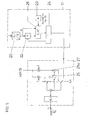
- a demodulator 1 exists as exemplary circuitry for determining symbols, Se from a digitized signal sd, which to a Quadrature signal pair of a modulation method, z. B. according to a QAM standard, from a variety of individual components. These can all or individually also component an integrated circuit. In particular are components described below depending on the purpose can be omitted or supplemented with other components. Also is the Continuation of signals as real signals, complex signals or individual complex signal components depending on the application and special circuitry adaptable accordingly.
- the demodulator receives 1 at an input from a signal source 2, for example a tuner, an analog signal sa.
- a signal source 2 for example a tuner
- an analog signal sa which is usually in a band-limited intermediate frequency position is present, an AD converter 3 (AD: analog / digital) supplied for conversion into a digital signal sd.
- the digital signal sd is the AD converter 3 to a Bandpass filter 5 out, which the digital signal of DC components and interfering harmonics released.
- the signal output from the bandpass filter 5 is supplied to a quadrature converter 6, which converts the digital signal sd into the baseband.
- the baseband corresponds to the requirements of the demodulator 1 and the modulation method used. Accordingly, the quadrature converter outputs the digitized signal sd split into the two quadrature signal components I, Q of the Cartesian coordinate system.
- the quadrature converter 6 is usually fed with two carriers offset by 90 ° from a local oscillator 7 whose frequency and phase are controlled by a carrier control device 8.
- the quadrature signal components I, Q are supplied to a low-pass filter 9, which serves to eliminate interfering harmonics.
- the thus filtered quadrature signal pair I, Q or the two quadrature signal components I, Q are then fed to a symbol scanner 10.
- the control of the symbol scanner 10 via an input to which the sampling signal t i is supplied.
- the symbol sampling instants t i are based on the symbol frequency 1 / T and usually also on the exact phase position of the symbol Se contained in the received signal sd, S.
- the symbol sampling instants ti are in a sampling controller 27 generated from a switch Sch and the actual Function unit 27a exists.
- the output of the scanner 10 is determined by means of a Low pass filter 11 filtered with a Nyquist characteristics and a gain control device 12, which the mean signal strength to the expected value of the used Modulation mode controls and the control range of a symbol decider 15 optimally exploited. That of the gain control device 12 output signal is an equalizer (Equalizer) 14 supplied. Equalizer 14 frees the two Components of the quadrature signal pair I, Q of interfering distortions and provides a signal S at its output. The following will be scanned from such provided Signals by means of Symbolentscheiders 15, the symbols Se formed.
- the signal currents S and signal currents Se compared, in equalizer 14, to the filter coefficients in a phase error detector 18 in order to and to detect frequency errors of the carrier control and to control the carrier control device 8 accordingly, and in a scanning error detector 19, in the locked state To detect errors in the sampling frequency and sampling phase and to control the scanning control device 27 accordingly.
- the phase error detector 18 and the sampling error detector 19 get as inputs the output from the equalizer 14 Signal S and the output from the decision maker 15 icon Se fed.
- the detection circuit 17 consists of a plurality of components, which may also be partially or completely accommodated in a single integrated circuit or circuit component.
- the detection circuit 17 also has a circuit for determining the quality value 28, the at least the radius component R is supplied from the coordinate converter 20 and a signal G representing the quality of the sample, to a controller 24, which in turn a detected sampling phase control signal to the sampling controller 27 issues.
- the circuit stands for determining the quality value 28 with two memory devices 22 and 29 in Connection, wherein the first of these memory devices 22 also at least the radial component R is supplied, the the coordinate converter 20 outputs. This first storage device is created so that it from the supplied radial component R forms a density distribution.
- the second storage device 29 contains a table with set radii Ra - Ri contains.
- the controller 24 causes a proper operation and controls the individual components and processes according to hardware or software supported instructions.
- the controller C also functions individual of said components in whole or in part integrated in itself.
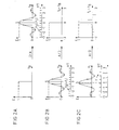
- FIGS. 2A-2C an ideal pulse diagram and an analog Nyquist wavelet are shown respectively on the right and left of a DA conversion process and an AD conversion process, respectively. Plotted are an amplitude E over the time axis t, on which the discrete base clock times t B are marked. Fig. 2C also shows a time axis with respect to the base clock t B offset actual sampling times t i .
- a pulse with the amplitude 1 and converted into an analog Nyquist wavelet (Fig. 2A).
- FIG. 2B is based on an ideally clocked sampling signal to the maximum central value of the wavelet, a sampling instant falls while the other sampling times respectively fall to zero crossings of the wavelet and thus no signal contribution deliver.
- the vector moves in phase space from one symbol code or Se to the next. Is he somewhere? on the track in between, he can not use a symbol code lie. Looking for the right positions for the pointer, which at a correctly determined sampling phase and sampling frequency.
- Fig. 2C is of a staggered Clock signal went out, where not the central, maximum Amplitude value of the wavelet, but instead one sampled lower amplitude value. After the scan is thus a central maximum amplitude value with a against the original amplitude reduced amplitude E output.
- the amplitudes of the adjacent ones Sampling signals whose time points are no longer accurate to the Zeros of the wavelet of the considered symbol fall, influenced by the considered symbol and vice versa, and the more so, the farther the sampling time from deviates ideal sampling.
- the symbol scanner 10 In the case of the non-ideal sampling according to FIG the symbol scanner 10 correspondingly interpolated samples available for further processing as data posed.
- the individual Nyquist pulses are superimposed intermittently and as I and Q components from the symbol scanner 10 issued.
- I, Q signal level which also represents the symbol code and phase plane by such samples, which deviate from the ideal times, Coordinates of points detected on the way of the phase vector from one symbol code to the next.
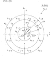
- FIG. 2D shows the Cartesian coordinate plane spanned by a quadrature signal pair I, Q, in which of 16 symbols S x, y of a 16-QAM signal the corresponding positions are drawn.
- the indices x, y correspond to the respective Cartesian coordinates, in which the 16 symbols would have to be determined with ideal sampling. Shown are also three circles Ka, Kb, Kc, on which the symbols S x, y are in accordance with the specifications of the 16-QAM method.
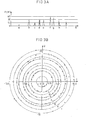
- Fig. 3A shows the distribution of the radius component R after the output of polar coordinates from the coordinate converter 20 in a 64-QAM system.
- the frequency of the radii of the signals S output by the equalizer 14 and converted by the coordinate converter 20 into polar coordinates is shown.
- the same also applies correspondingly to the use of the square R 2 of the radius component R.
- FIG. 3B illustrates the positions of particular and sampled signals in the 64-QAM system.
- circular rings a-i are also shown, which are defined by the radii R a given by the modulation system - R i are defined or fixed.
- FIGS. 3A and 3B results in a number of 8 symbols on the inner circle a, about 34 symbols on the subsequent circle b, and about 17, 33, 44, 39, 26 and 19 certain symbols on or in the area of the following Circular rings c - i.
- the illustrated frequency distribution of the radii of the scanned complex signals is the basic criterion for the quality signal or quality determination, since the radii in Unlike the Cartesian coordinates of neither Freguenzoffsets still dependent on phase offsets of the carrier control are. Therefore, for the beginning of a reception period, in the the support scheme has not yet locked in, taking into account the particular set radii of the respectively used Modulation method of sampling by the detection circuit 17 in the Abtastregel worn 27 systematically varies so that the Abtastgütesignal G is optimized and to achieve a correct sampling frequency and sampling phase position becomes.
- FIG. 4 An exemplary procedure starts according to FIG. 4 with the assumption that the carrier control 18, 8, 7, 6 shown in FIGS. 1 and 5 has not yet engaged, for which reason a switch Sch in the scanning control device 27 is brought into a first position "sync" becomes.
- the sampling frequency 1 / T is selected to correspond to the presumed symbol rate.
- the sampling phase can initially be chosen arbitrarily.
- the scanning signal t i generated in the scanning control device 27 is supplied to the scanning device 10 in the illustrated embodiment.
- the sampling phase can be adapted to the progress of the optimization become.
- the detection circuit 17 may be without knowledge get over the set radii and thus without memory unit 29, if to determine the scan quality after a trial in the memory device 22 present radii distribution an accumulation around especially discrete radii is investigated. This can z. B. with squaring of the individual frequencies and subsequent Summation done. The quality value G, G * is the better, the higher the sum.
- G * by means of a frequency distribution can the circuit for determining quality 28 also so be constructed such that the quality value G of the current sampling phase continuously by determining the quality value per symbol and by continued low-pass filtering of this result stream is determined.
- These are differences of the received radii to the nearest desired radius, whose values in the Memory unit 29 are held, determined and these radius differences low-pass filtered.
- the quality value G is thereby the better, the lower this result is.
- This z. B. areas hidden with many closely spaced radii or the amount of the difference per event is limited or otherwise weighted. This variant comes without the memory device 22 off.
- a comparison of the quality values offers itself G of attempts with something premature and a bit lagging Phase shift relative to the optimum sampling phase at.
- a steady change in the optimal timing of the sampling phase indicates a difference between transmitted symbol frequency and selected sampling frequency.
- Mathematically results the difference between transmitted symbol frequency and instantaneous Sampling frequency 1 / T from the derivative of the shift the optimal sampling phase.
- the control unit or controller 24 corrected the sampling interval T in the Abtastregel founded 27 by changing the the sampling control device 27 supplied control voltage.
- FIG. 5 shows an exemplary embodiment of the scanning control device 27. Essentially only individual components are described, to avoid repetition. Same reference numerals symbolize components or signals with the same or similar function and operation as described above is.
- the sampling control means 27 from a numerical oscillator 26, a double-pole switch Sch and a PI control filter, which in turn consists of two coefficient multipliers for the proportional (P) and integral (I) gain component, a Adder for merging the P and I controlled variables, one Adder 25a and a delay element 25 consists.
- the numerical oscillator is in the simplest case from an accumulator formed with modulo overflow. A previously defined Condition of the accumulator, z. B. 0 or overflow, generates the Sampling signal ti.
- the numerical oscillator 26 accumulates the input.
- a constantly applied quantity defines the frequency 1 / T of the sampling signal t i .
- An applied in only one system clock size causes a phase shift of the sampling signal ti.
- the controller 24 controls the numerical oscillator 26 and the contents of the delay element 25.
- the control device 24 selects after the one described above Method a sampling frequency by a constant and a Sampling phase by overlapping the angular difference once relative to the old sampling phase to said constant. The further procedure is as described above.
- the method can also be used in further exemplary arrangement possibilities for the circuit arrangement.
- a centrally controlled sampling and digitizing clock in the form of the sampling signal t i can be supplied to the AD converter 3 according to FIG. 1 by the clock control device.
- the sampling signal t i is finally synchronized exactly to that for the received symbol or signal sa.
- a later interpolation in the scanning device can be omitted as a separate functional unit (10 in FIG. 1).
- the low pass 9 after the quadrature converter 6 is no longer required. Its limiting effect takes the low pass 11 with the Nyquist characteristic.
- the carrier frequency of the circuit arrangement ie the demodulator 1 is not yet correct and therefore rotates the whole coordinate system of the circuit arrangement with respect to the coordinate system of the input signal. Therefore, the usual decision-feedback rules do not work yet. In the proposed procedure, this rotation can be ignored.
- the sampling clock needed in the A / D converter or in a subsequent purely numerical sampling rate conversion is not correct in phase, and possibly to a limited extent, in frequency.
- the aim of the procedure is to capture the sampling clock t i .
- the clock acquisition circuit 17 gives a clock acquisition Clock out, which still deviates in terms of phase and the Frequency has.
- n symbols are used to evaluate the distribution pattern.
- a tabular listing of several test sequences, each with a different phase, shows the increasing improvement of the specific clock signals after a continuous variation of the phase ⁇ by a phase difference ⁇ : Scan quality G Grid (R) ⁇ (S (R)) ⁇ (S (R) 2 ) bad 1 2 1 2 2 1 3 1 1 14 26 better 0 1 0 2 3 4 3 1 0 14 40 Good 0 0 0 4 6 4 0 0 0 14 68 very well 0 0 0 0 14 0 0 0 0 14 196
- the first column Shown in the first column is the improvement of the scan quality G.
- the second column represents the number of symbols per grid in a given grid distance around the target radius
- the third column shows that each one Totals of present 14 is determined when the entire radius surrounding the setpoint radius is considered around. It is therefore useful when considering the simple sum only the consideration of a preferably narrow range or a weighted area around the target radius R around. Becomes on the other hand, considering the square of the sum radii, yields even when looking at the entire grid area from the resulting value a noticeable improvement in the Scanning quality G.
- this procedure in principle independent of the actual position of the set radii, taking into account the gain.
- phase ⁇ from step to step Step can be an iterative improvement through further increase or lowering the phase value.
- the switch Sch After locking the carrier control, the switch Sch be routed, leaving a normal decision-feedback Scan control is used. As soon as the parallel Continuous sampling monitoring deterioration of the quality value detects, the switch Sch is again in the other Switched position to a tracking and correction of the sampling clock make.
- differences can also be considered determined symbols to the next target radius.
- a good phase of the scan is then at a small or not existing difference given.
- this method is also suitable in connection with low-pass filtering for a continuous measurement. The denomination in individual experiments then disappears.
- the method is thus based on that, with proper sampling all radii of the preliminary symbols fall on nominal radii, while in the times between the symbols the phase vector is on the way from one symbol to the next and, there usually another symbol is driven and there the signal Overall, low-pass filtered, the transitions thus soft are so that the phase vector is probably not on one Sollradius will be found.
- This method is advantageous completely independent of the state of the carrier regulation, because the angle information of the preliminary symbol is ignored becomes.
- the method can be done with experiments of n-symbols work. The n symbols can be used for different experiments be identical or be redefined. at This procedure does not deliver a control voltage, which correspond to the first derivative of the quality after the phase would. The control thus proceeds probatively.
- the tasting can be replaced by an indicated modulation of the scan angle, which is not optimal sampling a modulation with the same frequency of the product size leads. Furthermore, it is possible, the sampling circuit and subsequent Do blocks twice to allow early / late measurement. It is also possible to use a separate arrangement for the actual signal part as an additional arrangement of corresponding circuit elements.
Landscapes
- Engineering & Computer Science (AREA)
- Computer Networks & Wireless Communication (AREA)
- Signal Processing (AREA)
- Digital Transmission Methods That Use Modulated Carrier Waves (AREA)
- Amplitude Modulation (AREA)
- Time-Division Multiplex Systems (AREA)
Abstract
Description
- Fig. 1
- eine Schaltungsanordnung zum Bestimmen von Symbolen aus einem digitalisierten Signal, welches an zumindest ein Quadratursignalpaar eines Modulationsverfahrens gekoppelt ist, wobei die Schaltungsanordnung eine Einrichtung zum Bestimmen des Abtastzeitpunkts des Taktsignals aufweist und das Symbol bei freilaufendem A/D-Wandler über eine rein digitale Abtastratenwandlung gewonnen wird;
- Fig. 2A - 2C
- für sich bekannte Signaldarstellungen im digitalen und analogen Bereich eines Senders sowie mit richtiger Taktwahl und falscher Taktwahl eines Empfängers;
- Fig. 2D
- eine Darstellung der Symbolanordnung von 16-QAM im kartesischen komplexen Koordinatenraum;
- Fig. 3A, 3B:
- eine Häufigkeitsverteilung über dem Radius bzw. eine Signalverteilung in der komplexen polaren Symbolraumdarstellung von 64 QAM;
- Fig. 4
- ein Ablaufdiagramm zur Durchführung eines Verfahrens zur Abtastzeitpunkt-Bestimmung und
- Fig. 5
- einen detaillierteren Ausschnitt einer Detektionsschaltungsanordnung aus Fig. 1.
| Abtastgüte G | Raster (R) | Σ(S(R)) | Σ(S(R)2) | ||||||||
| schlecht | 1 | 2 | 1 | 2 | 2 | 1 | 3 | 1 | 1 | 14 | 26 |
| besser | 0 | 1 | 0 | 2 | 3 | 4 | 3 | 1 | 0 | 14 | 40 |
| gut | 0 | 0 | 0 | 4 | 6 | 4 | 0 | 0 | 0 | 14 | 68 |
| sehr gut | 0 | 0 | 0 | 0 | 14 | 0 | 0 | 0 | 0 | 14 | 196 |
Claims (14)
- Verfahren zum Bestimmen eines Abtastzeitpunkts eines Taktsignals (t; T) für eine Schaltungsanordnung (1; 1') zum Bestimmen von Symbolen (Se) mit diskreten Amplituden aus einem digitalisierten Signal (sd, S) eines Modulationsverfahrens (QAM) mit dem Schritt:gekennzeichnet durch die Schritte:a) Umsetzen des digitalisierten und demodulierten Signals (S) in eine radiale Komponente (R, S1, S2),b) Bestimmen eines Gütewertes (G) von Signalen (S) anhand einer radiusbezogenen Lage der Signale bei einer ersten Abtastphase (ϕi), welche relativ zu einem Basistaktzeitpunkt eines Basistaktes festgelegt ist (S2, S3),c) Bestimmen eines weiteren Gütewertes (G*) von Symbolen (S) bei einer relativ zu der vorherigen Abtastphase (ϕi) variierten Abtastphase (ϕi2 = ϕi + Δϕ) (S4, S5),d) Ermitteln des besseren der bestimmten Gütewerte (G, G*) (S6) unde) weiteres Verwenden der Abtastphase (ϕi oder ϕi2) des besseren Gütewerts (G bzw. G*) und/oderf) weiteres Variieren der Abtastphase (ϕi, ϕi2) (S6, S7, S8).
- Verfahren nach Anspruch 1, bei dem das Modulationsverfahren ein PSK- oder QAM-Verfahren oder ein demgegenüber höherwertiges Modulationsverfahren ist (PSK: Phase-Shift Keying, QAM: Quadratur Amplitude Modulation).
- Verfahren nach Anspruch 1 oder 2, bei dem aus Gütewerten (G, G*), welche in zeitlichen Abständen bestimmten Signalen (S) zugeordnet sind, und den dabei verwendeten Abtastphasen (ϕi bzw. ϕi2) eine Frequenzkorrektur bestimmt wird.
- Verfahren nach Anspruch 1 oder 2, bei dem das Bestimmen Gütewerte (G, G*) der Signale (S) zu aufeinanderfolgenden Zeitpunkten mit gleichen Abtastphasen (ϕi = ϕi2) durchgeführt wird und anhand einer Wertveränderung der Gütewerte (G, G*) eine erforderliche Frequenzkorrektur angezeigt wird.
- Verfahren nach einem vorstehenden Anspruch, bei dem die Gütewerte (G, G*) der Signale (S) abhängig von der Häufigkeitsverteilung der Signale (S) in der radialen Komponente (R) bestimmt werden.
- Verfahren nach Anspruch 5, bei dem die Gütewerte (G, G*) abhängig vom Quadrat der Häufigkeiten der Signale (S) und abhängig von der radialen Verteilung der Signale bestimmt werden.
- Verfahren nach einem vorstehenden Anspruch, bei dem die Gütewerte (G, G*) der Signale (S) im Bereich festgelegter Radien (Ra - Ri) des Modulationsverfahrens (QAM) in der polaren Signalkoordinatenebene (R, α) bestimmt werden.
- Verfahren nach einem vorstehenden Anspruch, bei dem die Gütewerte (G, G*) der Signale (S) im Bereich eines oder mehrerer ausgewählter Radien (Ra - Rc) aus einer Vielzahl von Radien des Modulationsverfahrens (QAM) bestimmt werden.
- Verfahren nach Anspruch 7 oder 8, bei dem die Gütewerte (G, G*) der Signale (S) nur in festgelegten Toleranzbereichen (ΔR) um die Radien (Rb) herum bestimmt werden.
- Verfahren nach einem der Ansprüche 5 bis 9, bei dem die Gütewerte (G, G*) der Signale (S) in Bereichen um die Radien (Ra - Ri) herum gewichtet bestimmt werden.
- Verfahren nach einem vorstehenden Anspruch, bei dem der Basistakt nach einer festgestellten erforderlichen Verschiebung des Abtastzeitpunktes gegenüber dem ursprünglichen Basistakt um eine entsprechende Differenztaktdauer verschoben wird.
- Verfahren nach einem vorstehenden Anspruch, bei dem bei einer kontinuierlichen Veränderung der über eine Vielzahl an Abtastzeitpunkten bestimmten Gütewerte (G, G*) die Taktdauer (T) des Basistaktes korrigiert wird.
- Schaltungsanordnung miteiner Taktsteuereinrichtung (17 - 29) zum Ausgeben von Taktsignalen (ti) zu diskreten Abtastzeitpunkten,einem Polarkoordinatenumsetzer (20; I, Q→R, α) zum Bestimmen zumindest einer radialen Koordinate (R) zu Signalen (S) aus einem digitalisierten Signal (sd) mit diskreten Amplituden eines Modulationsverfahrens (QAM),zumindest einem Speicher (M) zum Speichern von Betriebsparametern und radialen Komponenten (R) der Signale (S),einer Steuereinrichtung (C, 24) zum Steuern des Betriebsablaufs und Durchführen eines Verfahrens zum Bestimmen des Abtastzeitpunkts des Taktsignals (ti) gemäß einem der vorstehenden Ansprüche, wobeidie Steuereinrichtung (C, 24) und/oder weitere Komponenten (22, 28, 29) ausgebildet und ausgelegt sind- zum Variieren der Abtastphase (ϕi, ϕi2) gegenüber einem Basistaktzeitpunkt eines Basistaktes, und- zum Bestimmen von Gütewerten (G, G*) zu Signalen, welche mit verschiedenen variierten Abtastphasen (ϕi bzw. (ϕi2) bestimmt werden, und zwar insbesondere abhängig von der räumlichen Lage der bestimmten Signale (S) relativ zumindest einem Radius (Ra - Rc) im Koordinatensystem der radialen Koordinate.
- Schaltungsanordnung nach Anspruch 13 mit einer Schalteinrichtung (27, Sch) zum Bestimmen des Taktsignals (ti) wahlweise entsprechend einer entscheidungsrückgekoppelten Abtastregelung oder mit einem Wert einer variierten Abtastphase (ϕi, ϕi2).
Applications Claiming Priority (2)
| Application Number | Priority Date | Filing Date | Title |
|---|---|---|---|
| DE102004020300 | 2004-04-26 | ||
| DE102004020300A DE102004020300B3 (de) | 2004-04-26 | 2004-04-26 | Verfahren und Schaltungsanordnung zum Bestimmen eines Taktsignal-Abtastzeitpunkts für Symbole eines Modulationsverfahrens |
Publications (4)
| Publication Number | Publication Date |
|---|---|
| EP1592164A2 true EP1592164A2 (de) | 2005-11-02 |
| EP1592164A3 EP1592164A3 (de) | 2006-06-21 |
| EP1592164B1 EP1592164B1 (de) | 2010-06-16 |
| EP1592164B8 EP1592164B8 (de) | 2010-07-21 |
Family
ID=34877752
Family Applications (1)
| Application Number | Title | Priority Date | Filing Date |
|---|---|---|---|
| EP05008853A Expired - Lifetime EP1592164B8 (de) | 2004-04-26 | 2005-04-22 | Verfahren und Schaltungsanordnung zum Bestimmen eines Taktsignal-Abtastzeitpunkts für Symbole eines Modulationsverfahrens |
Country Status (4)
| Country | Link |
|---|---|
| US (1) | US7675998B2 (de) |
| EP (1) | EP1592164B8 (de) |
| AT (1) | ATE471610T1 (de) |
| DE (2) | DE102004020300B3 (de) |
Families Citing this family (15)
| Publication number | Priority date | Publication date | Assignee | Title |
|---|---|---|---|---|
| DE10344756A1 (de) * | 2003-09-25 | 2005-05-12 | Micronas Gmbh | Verfahren und Schaltungsanordnung zum Entscheiden eines Symbols im komplexen Phasenraum eines Quadraturmodulationsverfahrens |
| DE102006062519A1 (de) * | 2006-12-29 | 2008-07-03 | Micronas Gmbh | Vorrichtung und Verfahren zum Entscheiden eines Symbols beim Empfang eines mit einem Quadratursignalpaar gekoppelten Signals zur QAM-Frequenzregelung und/oder Rotationsregelung |
| WO2008087004A1 (de) * | 2007-01-16 | 2008-07-24 | Micronas Gmbh | Anwendung von vorläufig entschiedenen symbolen in einem quadraturempfänger |
| KR20080088302A (ko) * | 2007-03-29 | 2008-10-02 | 삼성전자주식회사 | 이상 변조 신호 처리 방법 및 이상 변조 신호 보상 기능을가지는 수신기 |
| DE102014209469A1 (de) * | 2014-05-19 | 2015-11-19 | TRUMPF Hüttinger GmbH + Co. KG | Regelungsanordnung, Regelsystem und Hochfrequenzleistungserzeugungsvorrichtung |
| EP3210034B1 (de) | 2014-10-24 | 2019-09-11 | Texas Instruments Incorporated | Batteriekapazitätsmonitor |
| US9553754B1 (en) | 2015-09-10 | 2017-01-24 | Qualcomm Incorporated | Post distortion in satellite communications |
| FR3046709B1 (fr) * | 2016-01-07 | 2019-06-14 | Commissariat A L'energie Atomique Et Aux Energies Alternatives | Recepteur rf a poursuite de frequence |
| US11398876B2 (en) | 2021-02-19 | 2022-07-26 | Ultralogic 6G, Llc | Error detection and correction in 5G/6G pulse-amplitude modulation |
| US11601150B1 (en) | 2021-11-17 | 2023-03-07 | Ultralogic 6G, Llc | Demodulation for phase-noise mitigation in 5G and 6G |
| US12250100B2 (en) * | 2022-02-14 | 2025-03-11 | David E. Newman | Selecting a modulation scheme responsive to fault types in 5G/6G |
| US11736320B2 (en) * | 2022-02-14 | 2023-08-22 | Ultralogic 6G, Llc | Multiplexed amplitude-phase modulation for 5G/6G noise mitigation |
| US11637649B2 (en) | 2022-09-06 | 2023-04-25 | Ultralogic 6G, Llc | Phase-noise mitigation at high frequencies in 5G and 6G |
| CN115550124B (zh) * | 2022-09-23 | 2024-09-13 | 中孚安全技术有限公司 | 一种信号调制方式识别方法及系统 |
| US11737044B1 (en) | 2022-12-12 | 2023-08-22 | Ultralogic 6G, Llc | Mid-symbol timestamp point for precision synchronization in 5G and 6G |
Family Cites Families (13)
| Publication number | Priority date | Publication date | Assignee | Title |
|---|---|---|---|---|
| DE3766614D1 (de) * | 1987-03-10 | 1991-01-17 | Ant Nachrichtentech | Verfahren zum gewinnen eines phasendifferenzsignals. |
| US4866739A (en) * | 1988-02-22 | 1989-09-12 | Silicon Systems, Inc. | Digital fast recovery timing algorithm |
| US5079512A (en) * | 1989-07-17 | 1992-01-07 | Nec Corporation | Quadrature demodulation of a data sequence following a particular signal sequence with a local reference carrier signal having a frequency different from a received carrier signal |
| US5513209A (en) * | 1993-02-26 | 1996-04-30 | Holm; Gunnar | Resampling synchronizer of digitally sampled signals |
| US5671257A (en) * | 1995-06-06 | 1997-09-23 | Sicom, Inc. | Symbol timing recovery based on complex sample magnitude |
| DE19540250C1 (de) * | 1995-10-28 | 1997-02-20 | Hermann Prof Dr Rer Na Rohling | Pseudokohärentes Demodulationsverfahren für ein verrauschtes, differentiell moduliertes Multiträgersignal |
| DE59609450D1 (de) * | 1996-01-26 | 2002-08-22 | Micronas Gmbh | Digitaler Demodulator |
| EP0895386B1 (de) * | 1997-07-31 | 2003-01-29 | Micronas Semiconductor Holding AG | Trägerregelkreis für einen Empfänger von digital übertragenen Signalen |
| US6154510A (en) * | 1999-05-03 | 2000-11-28 | Sicom, Inc. | Symbol timing recovery based on adjusted, phase-selected magnitude values |
| DE19920334A1 (de) * | 1999-05-03 | 2000-11-16 | Siemens Ag | Verfahren und Schaltungsanordnung zur Regelung des Abtasttakts eines phasenmodulierten Signals |
| JP4284774B2 (ja) * | 1999-09-07 | 2009-06-24 | ソニー株式会社 | 送信装置、受信装置、通信システム、送信方法及び通信方法 |
| FR2847101B1 (fr) * | 2002-11-08 | 2005-09-23 | Thales Sa | Procede et modem pour la synchronisation et la poursuite de phase |
| DE10344756A1 (de) * | 2003-09-25 | 2005-05-12 | Micronas Gmbh | Verfahren und Schaltungsanordnung zum Entscheiden eines Symbols im komplexen Phasenraum eines Quadraturmodulationsverfahrens |
-
2004
- 2004-04-26 DE DE102004020300A patent/DE102004020300B3/de not_active Expired - Fee Related
-
2005
- 2005-04-22 US US11/112,875 patent/US7675998B2/en not_active Expired - Fee Related
- 2005-04-22 DE DE502005009743T patent/DE502005009743D1/de not_active Expired - Lifetime
- 2005-04-22 AT AT05008853T patent/ATE471610T1/de active
- 2005-04-22 EP EP05008853A patent/EP1592164B8/de not_active Expired - Lifetime
Non-Patent Citations (2)
| Title |
|---|
| "Entscheidungsrückgekoppelte Trägerphasenregelung im Basisband", pages: 429 - 431 |
| ENTSCHEIDUNGSRÜCKGEKOPPELTE TAKTREGELUNG, pages 213 - 215 |
Also Published As
| Publication number | Publication date |
|---|---|
| DE102004020300B3 (de) | 2005-09-22 |
| US7675998B2 (en) | 2010-03-09 |
| EP1592164B8 (de) | 2010-07-21 |
| EP1592164B1 (de) | 2010-06-16 |
| US20080112509A1 (en) | 2008-05-15 |
| ATE471610T1 (de) | 2010-07-15 |
| EP1592164A3 (de) | 2006-06-21 |
| DE502005009743D1 (de) | 2010-07-29 |
Similar Documents
| Publication | Publication Date | Title |
|---|---|---|
| DE69613007T2 (de) | Signalverarbeitungssystem | |
| EP1592164B1 (de) | Verfahren und Schaltungsanordnung zum Bestimmen eines Taktsignal-Abtastzeitpunkts für Symbole eines Modulationsverfahrens | |
| DE69534625T2 (de) | Mehrschwellendetektion für 0.3-GMSK | |
| DE2309167C2 (de) | Verfahren und Schaltungsanordnung zum Korrigieren eines durch Phasenzittern verfälschten elektrischen Übertragtungssignals | |
| EP0486554B1 (de) | Verfahren und vorrichtung zum umsetzen digital modulierter empfangssignale aus dem hochfrequenzbereich | |
| DE69406151T2 (de) | Einrichtung zur Synchronisierung eines lokalen Trägers, in OFDM-Systemen | |
| DE60002144T2 (de) | Vorrichtung und verfahren zur detektion falscher trägerverriegelung in einem empfänger | |
| DE2716979A1 (de) | Schaltungsanordnung fuer die korrektur von phasenjitter und frequenzversetzungen des in einem quadratur-amplituden-modulation-empfaenger empfangenen signals | |
| EP0829990B1 (de) | Verfahren zur Demodulation von höherstufigen MQAM-Signalen ohne Kenntnis der übertragenen Symbole | |
| DE69729329T2 (de) | Gerät und verfahren zur phasenschätzung | |
| DD292788A5 (de) | Verfahren und einrichtung zur automatischen frequenzregelung | |
| DE68928362T2 (de) | Digitale selbsttätige Frequenzsteuerung mit reinen Sinuswellen | |
| DE102004047398B3 (de) | Gemeinsamer Detektor für Taktphase und Trägerphase | |
| EP1523144A2 (de) | Verfahren und Schaltungsanordnung zum Entscheiden eines Symbols im komplexen Phasenraum eines Quadratumodulationsverfahrens | |
| DE3789984T2 (de) | Rauschsignaldetektion durch Abtastung des digitalen Grundfrequenzsignals an einer Augenöffnung. | |
| DE102007056490A1 (de) | Verfahren und Schaltungsanordnung zum Entscheiden eines Symbols beim Empfang von mit einem Quadratursignalpaar gekoppelten empfangenen Symbolen | |
| EP1556986B1 (de) | Verfahren und schaltung zur erzeugung eines hilfssymbols zum einregeln eines qam-demodulators | |
| EP1523146A2 (de) | Verfahren zum Synchronisieren einer Schaltungsanordnung beim Empfang eines modulierten Signals | |
| DE69838481T2 (de) | Schaltung zur Trägerwiederherstellung | |
| EP1892910A2 (de) | Verfahren bzw. Schaltungsanordnung zum Entscheiden eines Symbols beim Empfang eines mit einem Quadratur-Signalpaar gekoppelten Signals | |
| EP1596552A2 (de) | Verfahren und Schaltungsanordnung zum Bestimmen der Frequenz eines empfangenen Signals | |
| EP1490962B1 (de) | Demodulation eines digital frequenzmodulierten analogen empfangssignals durch auswertung der zeitlichen abstände zwischen den nulldurchgängen | |
| DE10036703B4 (de) | Verfahren und Vorrichtung zur Korrektur eines Resamplers | |
| DE102004036464B4 (de) | Trägerphasendetektor | |
| DE69433267T2 (de) | Digital synchronisierter diversity-funkempfänger |
Legal Events
| Date | Code | Title | Description |
|---|---|---|---|
| PUAI | Public reference made under article 153(3) epc to a published international application that has entered the european phase |
Free format text: ORIGINAL CODE: 0009012 |
|
| AK | Designated contracting states |
Kind code of ref document: A2 Designated state(s): AT BE BG CH CY CZ DE DK EE ES FI FR GB GR HU IE IS IT LI LT LU MC NL PL PT RO SE SI SK TR |
|
| AX | Request for extension of the european patent |
Extension state: AL BA HR LV MK YU |
|
| RIN1 | Information on inventor provided before grant (corrected) |
Inventor name: WITTE, FRANZ-OTTO, DR. Inventor name: NOESKE, CARSTEN, DIPL.-ING. Inventor name: BOCK, CHRISTIAN, DR. |
|
| PUAL | Search report despatched |
Free format text: ORIGINAL CODE: 0009013 |
|
| AK | Designated contracting states |
Kind code of ref document: A3 Designated state(s): AT BE BG CH CY CZ DE DK EE ES FI FR GB GR HU IE IS IT LI LT LU MC NL PL PT RO SE SI SK TR |
|
| AX | Request for extension of the european patent |
Extension state: AL BA HR LV MK YU |
|
| RIC1 | Information provided on ipc code assigned before grant |
Ipc: H04L 27/26 20060101ALN20060516BHEP Ipc: H04L 7/02 20060101AFI20050606BHEP Ipc: H04L 27/38 20060101ALI20060516BHEP |
|
| 17P | Request for examination filed |
Effective date: 20060718 |
|
| 17Q | First examination report despatched |
Effective date: 20060918 |
|
| AKX | Designation fees paid |
Designated state(s): AT BE BG CH CY CZ DE DK EE ES FI FR GB GR HU IE IS IT LI LT LU MC NL PL PT RO SE SI SK TR |
|
| 17Q | First examination report despatched |
Effective date: 20060918 |
|
| RAP1 | Party data changed (applicant data changed or rights of an application transferred) |
Owner name: TRIDENT MICROSYSTEMS (FAR EAST) LTD. |
|
| GRAP | Despatch of communication of intention to grant a patent |
Free format text: ORIGINAL CODE: EPIDOSNIGR1 |
|
| RIN1 | Information on inventor provided before grant (corrected) |
Inventor name: BOCK, CHRISTIAN, DR. Inventor name: NOESKE, CARSTEN, DIPL.-ING. Inventor name: WITTE, FRANZ-OTTO, DR. |
|
| GRAS | Grant fee paid |
Free format text: ORIGINAL CODE: EPIDOSNIGR3 |
|
| GRAA | (expected) grant |
Free format text: ORIGINAL CODE: 0009210 |
|
| AK | Designated contracting states |
Kind code of ref document: B1 Designated state(s): AT BE BG CH CY CZ DE DK EE ES FI FR GB GR HU IE IS IT LI LT LU MC NL PL PT RO SE SI SK TR |
|
| REG | Reference to a national code |
Ref country code: CH Ref legal event code: EP |
|
| RBV | Designated contracting states (corrected) |
Designated state(s): AT BE BG CH CY CZ DK EE ES FI FR GB GR HU IE IS IT LI LT LU MC NL PL PT RO SE SI SK TR |
|
| REG | Reference to a national code |
Ref country code: IE Ref legal event code: FG4D Free format text: LANGUAGE OF EP DOCUMENT: GERMAN |
|
| REF | Corresponds to: |
Ref document number: 502005009743 Country of ref document: DE Date of ref document: 20100729 Kind code of ref document: P |
|
| RIN2 | Information on inventor provided after grant (corrected) |
Inventor name: NOESKE, CARSTEN, DIPL.-ING. Inventor name: BOCK, CHRISTIAN, DR. Inventor name: WITTE, FRANZ-OTTO, DR. |
|
| REG | Reference to a national code |
Ref country code: NL Ref legal event code: VDEP Effective date: 20100616 |
|
| PG25 | Lapsed in a contracting state [announced via postgrant information from national office to epo] |
Ref country code: SE Free format text: LAPSE BECAUSE OF FAILURE TO SUBMIT A TRANSLATION OF THE DESCRIPTION OR TO PAY THE FEE WITHIN THE PRESCRIBED TIME-LIMIT Effective date: 20100616 Ref country code: LT Free format text: LAPSE BECAUSE OF FAILURE TO SUBMIT A TRANSLATION OF THE DESCRIPTION OR TO PAY THE FEE WITHIN THE PRESCRIBED TIME-LIMIT Effective date: 20100616 |
|
| LTIE | Lt: invalidation of european patent or patent extension |
Effective date: 20100616 |
|
| PG25 | Lapsed in a contracting state [announced via postgrant information from national office to epo] |
Ref country code: SI Free format text: LAPSE BECAUSE OF FAILURE TO SUBMIT A TRANSLATION OF THE DESCRIPTION OR TO PAY THE FEE WITHIN THE PRESCRIBED TIME-LIMIT Effective date: 20100616 Ref country code: FI Free format text: LAPSE BECAUSE OF FAILURE TO SUBMIT A TRANSLATION OF THE DESCRIPTION OR TO PAY THE FEE WITHIN THE PRESCRIBED TIME-LIMIT Effective date: 20100616 |
|
| PG25 | Lapsed in a contracting state [announced via postgrant information from national office to epo] |
Ref country code: PL Free format text: LAPSE BECAUSE OF FAILURE TO SUBMIT A TRANSLATION OF THE DESCRIPTION OR TO PAY THE FEE WITHIN THE PRESCRIBED TIME-LIMIT Effective date: 20100616 Ref country code: GR Free format text: LAPSE BECAUSE OF FAILURE TO SUBMIT A TRANSLATION OF THE DESCRIPTION OR TO PAY THE FEE WITHIN THE PRESCRIBED TIME-LIMIT Effective date: 20100917 Ref country code: CY Free format text: LAPSE BECAUSE OF FAILURE TO SUBMIT A TRANSLATION OF THE DESCRIPTION OR TO PAY THE FEE WITHIN THE PRESCRIBED TIME-LIMIT Effective date: 20100616 |
|
| REG | Reference to a national code |
Ref country code: IE Ref legal event code: FD4D |
|
| PG25 | Lapsed in a contracting state [announced via postgrant information from national office to epo] |
Ref country code: NL Free format text: LAPSE BECAUSE OF FAILURE TO SUBMIT A TRANSLATION OF THE DESCRIPTION OR TO PAY THE FEE WITHIN THE PRESCRIBED TIME-LIMIT Effective date: 20100616 Ref country code: EE Free format text: LAPSE BECAUSE OF FAILURE TO SUBMIT A TRANSLATION OF THE DESCRIPTION OR TO PAY THE FEE WITHIN THE PRESCRIBED TIME-LIMIT Effective date: 20100616 Ref country code: IE Free format text: LAPSE BECAUSE OF FAILURE TO SUBMIT A TRANSLATION OF THE DESCRIPTION OR TO PAY THE FEE WITHIN THE PRESCRIBED TIME-LIMIT Effective date: 20100616 |
|
| PG25 | Lapsed in a contracting state [announced via postgrant information from national office to epo] |
Ref country code: RO Free format text: LAPSE BECAUSE OF FAILURE TO SUBMIT A TRANSLATION OF THE DESCRIPTION OR TO PAY THE FEE WITHIN THE PRESCRIBED TIME-LIMIT Effective date: 20100616 Ref country code: SK Free format text: LAPSE BECAUSE OF FAILURE TO SUBMIT A TRANSLATION OF THE DESCRIPTION OR TO PAY THE FEE WITHIN THE PRESCRIBED TIME-LIMIT Effective date: 20100616 Ref country code: CZ Free format text: LAPSE BECAUSE OF FAILURE TO SUBMIT A TRANSLATION OF THE DESCRIPTION OR TO PAY THE FEE WITHIN THE PRESCRIBED TIME-LIMIT Effective date: 20100616 Ref country code: IS Free format text: LAPSE BECAUSE OF FAILURE TO SUBMIT A TRANSLATION OF THE DESCRIPTION OR TO PAY THE FEE WITHIN THE PRESCRIBED TIME-LIMIT Effective date: 20101016 Ref country code: PT Free format text: LAPSE BECAUSE OF FAILURE TO SUBMIT A TRANSLATION OF THE DESCRIPTION OR TO PAY THE FEE WITHIN THE PRESCRIBED TIME-LIMIT Effective date: 20101018 |
|
| PG25 | Lapsed in a contracting state [announced via postgrant information from national office to epo] |
Ref country code: IT Free format text: LAPSE BECAUSE OF FAILURE TO SUBMIT A TRANSLATION OF THE DESCRIPTION OR TO PAY THE FEE WITHIN THE PRESCRIBED TIME-LIMIT Effective date: 20100616 |
|
| PLBE | No opposition filed within time limit |
Free format text: ORIGINAL CODE: 0009261 |
|
| STAA | Information on the status of an ep patent application or granted ep patent |
Free format text: STATUS: NO OPPOSITION FILED WITHIN TIME LIMIT |
|
| PG25 | Lapsed in a contracting state [announced via postgrant information from national office to epo] |
Ref country code: DK Free format text: LAPSE BECAUSE OF FAILURE TO SUBMIT A TRANSLATION OF THE DESCRIPTION OR TO PAY THE FEE WITHIN THE PRESCRIBED TIME-LIMIT Effective date: 20100616 |
|
| 26N | No opposition filed |
Effective date: 20110317 |
|
| BERE | Be: lapsed |
Owner name: TRIDENT MICROSYSTEMS (FAR EAST) LTD. Effective date: 20110430 |
|
| PG25 | Lapsed in a contracting state [announced via postgrant information from national office to epo] |
Ref country code: MC Free format text: LAPSE BECAUSE OF NON-PAYMENT OF DUE FEES Effective date: 20110430 |
|
| REG | Reference to a national code |
Ref country code: CH Ref legal event code: PL |
|
| REG | Reference to a national code |
Ref country code: FR Ref legal event code: ST Effective date: 20111230 |
|
| PG25 | Lapsed in a contracting state [announced via postgrant information from national office to epo] |
Ref country code: BE Free format text: LAPSE BECAUSE OF NON-PAYMENT OF DUE FEES Effective date: 20110430 Ref country code: CH Free format text: LAPSE BECAUSE OF NON-PAYMENT OF DUE FEES Effective date: 20110430 Ref country code: LI Free format text: LAPSE BECAUSE OF NON-PAYMENT OF DUE FEES Effective date: 20110430 Ref country code: FR Free format text: LAPSE BECAUSE OF NON-PAYMENT OF DUE FEES Effective date: 20110502 |
|
| REG | Reference to a national code |
Ref country code: AT Ref legal event code: MM01 Ref document number: 471610 Country of ref document: AT Kind code of ref document: T Effective date: 20110422 |
|
| PG25 | Lapsed in a contracting state [announced via postgrant information from national office to epo] |
Ref country code: AT Free format text: LAPSE BECAUSE OF NON-PAYMENT OF DUE FEES Effective date: 20110422 |
|
| PG25 | Lapsed in a contracting state [announced via postgrant information from national office to epo] |
Ref country code: LU Free format text: LAPSE BECAUSE OF NON-PAYMENT OF DUE FEES Effective date: 20110422 |
|
| PGFP | Annual fee paid to national office [announced via postgrant information from national office to epo] |
Ref country code: GB Payment date: 20130429 Year of fee payment: 9 |
|
| PG25 | Lapsed in a contracting state [announced via postgrant information from national office to epo] |
Ref country code: TR Free format text: LAPSE BECAUSE OF FAILURE TO SUBMIT A TRANSLATION OF THE DESCRIPTION OR TO PAY THE FEE WITHIN THE PRESCRIBED TIME-LIMIT Effective date: 20100616 Ref country code: BG Free format text: LAPSE BECAUSE OF FAILURE TO SUBMIT A TRANSLATION OF THE DESCRIPTION OR TO PAY THE FEE WITHIN THE PRESCRIBED TIME-LIMIT Effective date: 20100916 |
|
| PG25 | Lapsed in a contracting state [announced via postgrant information from national office to epo] |
Ref country code: HU Free format text: LAPSE BECAUSE OF FAILURE TO SUBMIT A TRANSLATION OF THE DESCRIPTION OR TO PAY THE FEE WITHIN THE PRESCRIBED TIME-LIMIT Effective date: 20100616 Ref country code: ES Free format text: LAPSE BECAUSE OF FAILURE TO SUBMIT A TRANSLATION OF THE DESCRIPTION OR TO PAY THE FEE WITHIN THE PRESCRIBED TIME-LIMIT Effective date: 20100927 |
|
| REG | Reference to a national code |
Ref country code: GB Ref legal event code: 732E Free format text: REGISTERED BETWEEN 20131107 AND 20131113 |
|
| GBPC | Gb: european patent ceased through non-payment of renewal fee |
Effective date: 20140422 |
|
| PG25 | Lapsed in a contracting state [announced via postgrant information from national office to epo] |
Ref country code: GB Free format text: LAPSE BECAUSE OF NON-PAYMENT OF DUE FEES Effective date: 20140422 |