EP1592003A1 - Optical recording medium and method for manufacturing same - Google Patents
Optical recording medium and method for manufacturing same Download PDFInfo
- Publication number
- EP1592003A1 EP1592003A1 EP04704344A EP04704344A EP1592003A1 EP 1592003 A1 EP1592003 A1 EP 1592003A1 EP 04704344 A EP04704344 A EP 04704344A EP 04704344 A EP04704344 A EP 04704344A EP 1592003 A1 EP1592003 A1 EP 1592003A1
- Authority
- EP
- European Patent Office
- Prior art keywords
- layer
- less
- recording medium
- dielectrics
- optical recording
- Prior art date
- Legal status (The legal status is an assumption and is not a legal conclusion. Google has not performed a legal analysis and makes no representation as to the accuracy of the status listed.)
- Granted
Links
Images


Classifications
-
- G—PHYSICS
- G11—INFORMATION STORAGE
- G11B—INFORMATION STORAGE BASED ON RELATIVE MOVEMENT BETWEEN RECORD CARRIER AND TRANSDUCER
- G11B7/00—Recording or reproducing by optical means, e.g. recording using a thermal beam of optical radiation by modifying optical properties or the physical structure, reproducing using an optical beam at lower power by sensing optical properties; Record carriers therefor
- G11B7/24—Record carriers characterised by shape, structure or physical properties, or by the selection of the material
- G11B7/241—Record carriers characterised by shape, structure or physical properties, or by the selection of the material characterised by the selection of the material
- G11B7/242—Record carriers characterised by shape, structure or physical properties, or by the selection of the material characterised by the selection of the material of recording layers
- G11B7/243—Record carriers characterised by shape, structure or physical properties, or by the selection of the material characterised by the selection of the material of recording layers comprising inorganic materials only, e.g. ablative layers
- G11B7/2433—Metals or elements of groups 13, 14, 15 or 16 of the Periodic System, e.g. B, Si, Ge, As, Sb, Bi, Se or Te
-
- G—PHYSICS
- G11—INFORMATION STORAGE
- G11B—INFORMATION STORAGE BASED ON RELATIVE MOVEMENT BETWEEN RECORD CARRIER AND TRANSDUCER
- G11B7/00—Recording or reproducing by optical means, e.g. recording using a thermal beam of optical radiation by modifying optical properties or the physical structure, reproducing using an optical beam at lower power by sensing optical properties; Record carriers therefor
- G11B7/24—Record carriers characterised by shape, structure or physical properties, or by the selection of the material
- G11B7/241—Record carriers characterised by shape, structure or physical properties, or by the selection of the material characterised by the selection of the material
- G11B7/252—Record carriers characterised by shape, structure or physical properties, or by the selection of the material characterised by the selection of the material of layers other than recording layers
- G11B7/256—Record carriers characterised by shape, structure or physical properties, or by the selection of the material characterised by the selection of the material of layers other than recording layers of layers improving adhesion between layers
-
- G—PHYSICS
- G11—INFORMATION STORAGE
- G11B—INFORMATION STORAGE BASED ON RELATIVE MOVEMENT BETWEEN RECORD CARRIER AND TRANSDUCER
- G11B7/00—Recording or reproducing by optical means, e.g. recording using a thermal beam of optical radiation by modifying optical properties or the physical structure, reproducing using an optical beam at lower power by sensing optical properties; Record carriers therefor
- G11B7/24—Record carriers characterised by shape, structure or physical properties, or by the selection of the material
- G11B7/241—Record carriers characterised by shape, structure or physical properties, or by the selection of the material characterised by the selection of the material
- G11B7/252—Record carriers characterised by shape, structure or physical properties, or by the selection of the material characterised by the selection of the material of layers other than recording layers
- G11B7/257—Record carriers characterised by shape, structure or physical properties, or by the selection of the material characterised by the selection of the material of layers other than recording layers of layers having properties involved in recording or reproduction, e.g. optical interference layers or sensitising layers or dielectric layers, which are protecting the recording layers
- G11B7/2578—Record carriers characterised by shape, structure or physical properties, or by the selection of the material characterised by the selection of the material of layers other than recording layers of layers having properties involved in recording or reproduction, e.g. optical interference layers or sensitising layers or dielectric layers, which are protecting the recording layers consisting essentially of inorganic materials
-
- G—PHYSICS
- G11—INFORMATION STORAGE
- G11B—INFORMATION STORAGE BASED ON RELATIVE MOVEMENT BETWEEN RECORD CARRIER AND TRANSDUCER
- G11B7/00—Recording or reproducing by optical means, e.g. recording using a thermal beam of optical radiation by modifying optical properties or the physical structure, reproducing using an optical beam at lower power by sensing optical properties; Record carriers therefor
- G11B7/24—Record carriers characterised by shape, structure or physical properties, or by the selection of the material
- G11B7/26—Apparatus or processes specially adapted for the manufacture of record carriers
-
- G—PHYSICS
- G11—INFORMATION STORAGE
- G11B—INFORMATION STORAGE BASED ON RELATIVE MOVEMENT BETWEEN RECORD CARRIER AND TRANSDUCER
- G11B7/00—Recording or reproducing by optical means, e.g. recording using a thermal beam of optical radiation by modifying optical properties or the physical structure, reproducing using an optical beam at lower power by sensing optical properties; Record carriers therefor
- G11B7/24—Record carriers characterised by shape, structure or physical properties, or by the selection of the material
- G11B7/241—Record carriers characterised by shape, structure or physical properties, or by the selection of the material characterised by the selection of the material
- G11B7/242—Record carriers characterised by shape, structure or physical properties, or by the selection of the material characterised by the selection of the material of recording layers
- G11B7/243—Record carriers characterised by shape, structure or physical properties, or by the selection of the material characterised by the selection of the material of recording layers comprising inorganic materials only, e.g. ablative layers
- G11B2007/24302—Metals or metalloids
- G11B2007/24312—Metals or metalloids group 14 elements (e.g. Si, Ge, Sn)
-
- G—PHYSICS
- G11—INFORMATION STORAGE
- G11B—INFORMATION STORAGE BASED ON RELATIVE MOVEMENT BETWEEN RECORD CARRIER AND TRANSDUCER
- G11B7/00—Recording or reproducing by optical means, e.g. recording using a thermal beam of optical radiation by modifying optical properties or the physical structure, reproducing using an optical beam at lower power by sensing optical properties; Record carriers therefor
- G11B7/24—Record carriers characterised by shape, structure or physical properties, or by the selection of the material
- G11B7/241—Record carriers characterised by shape, structure or physical properties, or by the selection of the material characterised by the selection of the material
- G11B7/242—Record carriers characterised by shape, structure or physical properties, or by the selection of the material characterised by the selection of the material of recording layers
- G11B7/243—Record carriers characterised by shape, structure or physical properties, or by the selection of the material characterised by the selection of the material of recording layers comprising inorganic materials only, e.g. ablative layers
- G11B2007/24302—Metals or metalloids
- G11B2007/24314—Metals or metalloids group 15 elements (e.g. Sb, Bi)
-
- G—PHYSICS
- G11—INFORMATION STORAGE
- G11B—INFORMATION STORAGE BASED ON RELATIVE MOVEMENT BETWEEN RECORD CARRIER AND TRANSDUCER
- G11B7/00—Recording or reproducing by optical means, e.g. recording using a thermal beam of optical radiation by modifying optical properties or the physical structure, reproducing using an optical beam at lower power by sensing optical properties; Record carriers therefor
- G11B7/24—Record carriers characterised by shape, structure or physical properties, or by the selection of the material
- G11B7/241—Record carriers characterised by shape, structure or physical properties, or by the selection of the material characterised by the selection of the material
- G11B7/242—Record carriers characterised by shape, structure or physical properties, or by the selection of the material characterised by the selection of the material of recording layers
- G11B7/243—Record carriers characterised by shape, structure or physical properties, or by the selection of the material characterised by the selection of the material of recording layers comprising inorganic materials only, e.g. ablative layers
- G11B2007/24302—Metals or metalloids
- G11B2007/24316—Metals or metalloids group 16 elements (i.e. chalcogenides, Se, Te)
-
- G—PHYSICS
- G11—INFORMATION STORAGE
- G11B—INFORMATION STORAGE BASED ON RELATIVE MOVEMENT BETWEEN RECORD CARRIER AND TRANSDUCER
- G11B7/00—Recording or reproducing by optical means, e.g. recording using a thermal beam of optical radiation by modifying optical properties or the physical structure, reproducing using an optical beam at lower power by sensing optical properties; Record carriers therefor
- G11B7/24—Record carriers characterised by shape, structure or physical properties, or by the selection of the material
- G11B7/241—Record carriers characterised by shape, structure or physical properties, or by the selection of the material characterised by the selection of the material
- G11B7/252—Record carriers characterised by shape, structure or physical properties, or by the selection of the material characterised by the selection of the material of layers other than recording layers
- G11B7/257—Record carriers characterised by shape, structure or physical properties, or by the selection of the material characterised by the selection of the material of layers other than recording layers of layers having properties involved in recording or reproduction, e.g. optical interference layers or sensitising layers or dielectric layers, which are protecting the recording layers
- G11B2007/25705—Record carriers characterised by shape, structure or physical properties, or by the selection of the material characterised by the selection of the material of layers other than recording layers of layers having properties involved in recording or reproduction, e.g. optical interference layers or sensitising layers or dielectric layers, which are protecting the recording layers consisting essentially of inorganic materials
- G11B2007/25706—Record carriers characterised by shape, structure or physical properties, or by the selection of the material characterised by the selection of the material of layers other than recording layers of layers having properties involved in recording or reproduction, e.g. optical interference layers or sensitising layers or dielectric layers, which are protecting the recording layers consisting essentially of inorganic materials containing transition metal elements (Zn, Fe, Co, Ni, Pt)
-
- G—PHYSICS
- G11—INFORMATION STORAGE
- G11B—INFORMATION STORAGE BASED ON RELATIVE MOVEMENT BETWEEN RECORD CARRIER AND TRANSDUCER
- G11B7/00—Recording or reproducing by optical means, e.g. recording using a thermal beam of optical radiation by modifying optical properties or the physical structure, reproducing using an optical beam at lower power by sensing optical properties; Record carriers therefor
- G11B7/24—Record carriers characterised by shape, structure or physical properties, or by the selection of the material
- G11B7/241—Record carriers characterised by shape, structure or physical properties, or by the selection of the material characterised by the selection of the material
- G11B7/252—Record carriers characterised by shape, structure or physical properties, or by the selection of the material characterised by the selection of the material of layers other than recording layers
- G11B7/257—Record carriers characterised by shape, structure or physical properties, or by the selection of the material characterised by the selection of the material of layers other than recording layers of layers having properties involved in recording or reproduction, e.g. optical interference layers or sensitising layers or dielectric layers, which are protecting the recording layers
- G11B2007/25705—Record carriers characterised by shape, structure or physical properties, or by the selection of the material characterised by the selection of the material of layers other than recording layers of layers having properties involved in recording or reproduction, e.g. optical interference layers or sensitising layers or dielectric layers, which are protecting the recording layers consisting essentially of inorganic materials
- G11B2007/2571—Record carriers characterised by shape, structure or physical properties, or by the selection of the material characterised by the selection of the material of layers other than recording layers of layers having properties involved in recording or reproduction, e.g. optical interference layers or sensitising layers or dielectric layers, which are protecting the recording layers consisting essentially of inorganic materials containing group 14 elements except carbon (Si, Ge, Sn, Pb)
-
- G—PHYSICS
- G11—INFORMATION STORAGE
- G11B—INFORMATION STORAGE BASED ON RELATIVE MOVEMENT BETWEEN RECORD CARRIER AND TRANSDUCER
- G11B7/00—Recording or reproducing by optical means, e.g. recording using a thermal beam of optical radiation by modifying optical properties or the physical structure, reproducing using an optical beam at lower power by sensing optical properties; Record carriers therefor
- G11B7/24—Record carriers characterised by shape, structure or physical properties, or by the selection of the material
- G11B7/241—Record carriers characterised by shape, structure or physical properties, or by the selection of the material characterised by the selection of the material
- G11B7/252—Record carriers characterised by shape, structure or physical properties, or by the selection of the material characterised by the selection of the material of layers other than recording layers
- G11B7/257—Record carriers characterised by shape, structure or physical properties, or by the selection of the material characterised by the selection of the material of layers other than recording layers of layers having properties involved in recording or reproduction, e.g. optical interference layers or sensitising layers or dielectric layers, which are protecting the recording layers
- G11B2007/25705—Record carriers characterised by shape, structure or physical properties, or by the selection of the material characterised by the selection of the material of layers other than recording layers of layers having properties involved in recording or reproduction, e.g. optical interference layers or sensitising layers or dielectric layers, which are protecting the recording layers consisting essentially of inorganic materials
- G11B2007/25713—Record carriers characterised by shape, structure or physical properties, or by the selection of the material characterised by the selection of the material of layers other than recording layers of layers having properties involved in recording or reproduction, e.g. optical interference layers or sensitising layers or dielectric layers, which are protecting the recording layers consisting essentially of inorganic materials containing nitrogen
-
- G—PHYSICS
- G11—INFORMATION STORAGE
- G11B—INFORMATION STORAGE BASED ON RELATIVE MOVEMENT BETWEEN RECORD CARRIER AND TRANSDUCER
- G11B7/00—Recording or reproducing by optical means, e.g. recording using a thermal beam of optical radiation by modifying optical properties or the physical structure, reproducing using an optical beam at lower power by sensing optical properties; Record carriers therefor
- G11B7/24—Record carriers characterised by shape, structure or physical properties, or by the selection of the material
- G11B7/241—Record carriers characterised by shape, structure or physical properties, or by the selection of the material characterised by the selection of the material
- G11B7/252—Record carriers characterised by shape, structure or physical properties, or by the selection of the material characterised by the selection of the material of layers other than recording layers
- G11B7/257—Record carriers characterised by shape, structure or physical properties, or by the selection of the material characterised by the selection of the material of layers other than recording layers of layers having properties involved in recording or reproduction, e.g. optical interference layers or sensitising layers or dielectric layers, which are protecting the recording layers
- G11B2007/25705—Record carriers characterised by shape, structure or physical properties, or by the selection of the material characterised by the selection of the material of layers other than recording layers of layers having properties involved in recording or reproduction, e.g. optical interference layers or sensitising layers or dielectric layers, which are protecting the recording layers consisting essentially of inorganic materials
- G11B2007/25715—Record carriers characterised by shape, structure or physical properties, or by the selection of the material characterised by the selection of the material of layers other than recording layers of layers having properties involved in recording or reproduction, e.g. optical interference layers or sensitising layers or dielectric layers, which are protecting the recording layers consisting essentially of inorganic materials containing oxygen
-
- G—PHYSICS
- G11—INFORMATION STORAGE
- G11B—INFORMATION STORAGE BASED ON RELATIVE MOVEMENT BETWEEN RECORD CARRIER AND TRANSDUCER
- G11B7/00—Recording or reproducing by optical means, e.g. recording using a thermal beam of optical radiation by modifying optical properties or the physical structure, reproducing using an optical beam at lower power by sensing optical properties; Record carriers therefor
- G11B7/24—Record carriers characterised by shape, structure or physical properties, or by the selection of the material
- G11B7/241—Record carriers characterised by shape, structure or physical properties, or by the selection of the material characterised by the selection of the material
- G11B7/252—Record carriers characterised by shape, structure or physical properties, or by the selection of the material characterised by the selection of the material of layers other than recording layers
- G11B7/257—Record carriers characterised by shape, structure or physical properties, or by the selection of the material characterised by the selection of the material of layers other than recording layers of layers having properties involved in recording or reproduction, e.g. optical interference layers or sensitising layers or dielectric layers, which are protecting the recording layers
- G11B2007/25705—Record carriers characterised by shape, structure or physical properties, or by the selection of the material characterised by the selection of the material of layers other than recording layers of layers having properties involved in recording or reproduction, e.g. optical interference layers or sensitising layers or dielectric layers, which are protecting the recording layers consisting essentially of inorganic materials
- G11B2007/25716—Record carriers characterised by shape, structure or physical properties, or by the selection of the material characterised by the selection of the material of layers other than recording layers of layers having properties involved in recording or reproduction, e.g. optical interference layers or sensitising layers or dielectric layers, which are protecting the recording layers consisting essentially of inorganic materials containing sulfur
-
- G—PHYSICS
- G11—INFORMATION STORAGE
- G11B—INFORMATION STORAGE BASED ON RELATIVE MOVEMENT BETWEEN RECORD CARRIER AND TRANSDUCER
- G11B7/00—Recording or reproducing by optical means, e.g. recording using a thermal beam of optical radiation by modifying optical properties or the physical structure, reproducing using an optical beam at lower power by sensing optical properties; Record carriers therefor
- G11B7/24—Record carriers characterised by shape, structure or physical properties, or by the selection of the material
- G11B7/241—Record carriers characterised by shape, structure or physical properties, or by the selection of the material characterised by the selection of the material
- G11B7/252—Record carriers characterised by shape, structure or physical properties, or by the selection of the material characterised by the selection of the material of layers other than recording layers
- G11B7/253—Record carriers characterised by shape, structure or physical properties, or by the selection of the material characterised by the selection of the material of layers other than recording layers of substrates
- G11B7/2531—Record carriers characterised by shape, structure or physical properties, or by the selection of the material characterised by the selection of the material of layers other than recording layers of substrates comprising glass
-
- G—PHYSICS
- G11—INFORMATION STORAGE
- G11B—INFORMATION STORAGE BASED ON RELATIVE MOVEMENT BETWEEN RECORD CARRIER AND TRANSDUCER
- G11B7/00—Recording or reproducing by optical means, e.g. recording using a thermal beam of optical radiation by modifying optical properties or the physical structure, reproducing using an optical beam at lower power by sensing optical properties; Record carriers therefor
- G11B7/24—Record carriers characterised by shape, structure or physical properties, or by the selection of the material
- G11B7/241—Record carriers characterised by shape, structure or physical properties, or by the selection of the material characterised by the selection of the material
- G11B7/252—Record carriers characterised by shape, structure or physical properties, or by the selection of the material characterised by the selection of the material of layers other than recording layers
- G11B7/253—Record carriers characterised by shape, structure or physical properties, or by the selection of the material characterised by the selection of the material of layers other than recording layers of substrates
- G11B7/2533—Record carriers characterised by shape, structure or physical properties, or by the selection of the material characterised by the selection of the material of layers other than recording layers of substrates comprising resins
- G11B7/2534—Record carriers characterised by shape, structure or physical properties, or by the selection of the material characterised by the selection of the material of layers other than recording layers of substrates comprising resins polycarbonates [PC]
-
- G—PHYSICS
- G11—INFORMATION STORAGE
- G11B—INFORMATION STORAGE BASED ON RELATIVE MOVEMENT BETWEEN RECORD CARRIER AND TRANSDUCER
- G11B7/00—Recording or reproducing by optical means, e.g. recording using a thermal beam of optical radiation by modifying optical properties or the physical structure, reproducing using an optical beam at lower power by sensing optical properties; Record carriers therefor
- G11B7/24—Record carriers characterised by shape, structure or physical properties, or by the selection of the material
- G11B7/241—Record carriers characterised by shape, structure or physical properties, or by the selection of the material characterised by the selection of the material
- G11B7/252—Record carriers characterised by shape, structure or physical properties, or by the selection of the material characterised by the selection of the material of layers other than recording layers
- G11B7/258—Record carriers characterised by shape, structure or physical properties, or by the selection of the material characterised by the selection of the material of layers other than recording layers of reflective layers
- G11B7/259—Record carriers characterised by shape, structure or physical properties, or by the selection of the material characterised by the selection of the material of layers other than recording layers of reflective layers based on silver
Definitions
- the present invention relates to an optical recording medium and a manufacturing method thereof, in particular, one that can be preferably applicable to an optical recording medium in which laser light is irradiated from a side on which a protective layer is disposed to protect an information signal portion, and thereby the information signal is recorded and reproduced.
- optical information recording system has many advantages in that (1) non-contact recording and/or reproducing can be realized, (2) the recording density more than one digit higher than that of a magnetic recording system can be attained, (3) less expensive and large capacity file can be realized and so on. Accordingly, a wide application from industrial uses to consumer uses is in consideration.
- Optical recording media that use the optical information recording system can be categorized into a read-only type, a rewrite type and a write-once type.
- the read-only type optical recording medium is the most popular optical recording medium at present, and as the optical recording medium, for instance, a CD-DA (CD-Digital Audio), a CD-ROM (Compact Disc Read Only Memory), a DVD-ROM (Digital Versatile Disc-Read Only Memory) and so on can be cited.
- the rewrite type optical recording medium is a recording medium in which information can be erased and rewritten and can be categorized into an optical magnetic recording medium and a phase change recording medium.
- the optical magnetic recording medium is a recording medium that makes use of thermal magnetic recording and magneto-optical reproducing, and, as the optical recording medium, for instance, an MO (Magneto Optical) and MD (Mini Disc) can be cited.
- the phase change recording medium is an optical recording medium that makes use of a structural phase change between crystalline and amorphous phases, and as the optical recording medium, for instance, a CD-RW (Compact Disc ReWritable) and a DVD-R (Digital Versatile Disc-Recordable) can be cited.
- the write-once type optical recording medium is an optical recording medium that allows neither erasing nor rewriting information but allows overwriting in another place, and as the optical recording medium, for instance, a CD-R (Compact Disc Recordable) and a DVD-R (Digital Versatile Disc-Recordable) can be cited.
- a CD-R Compact Disc Recordable
- DVD-R Digital Versatile Disc-Recordable
- optical recording medium can be roughly divided into a single plate type (for instance, CD, CD-R, and CD-RW) and a laminated type (for instance, DVD-ROM, DVD-R, and DVD-RW).
- the CD has a configuration in which on a transparent substrate on which a concaved pattern is formed in accordance with an information signal, a reflective layer made of aluminum and a protective layer that protects the reflective layer from moisture and oxygen in air are sequentially formed.
- the CD-RW has a configuration in which on one main surface of a transparent substrate on which a concave pattern such as a land and a groove is formed, a transparent dielectrics film made of silicon nitride, a phase change recording layer made of a chalcogen compound, a transparent dielectrics layer made of silicon nitride and a reflective layer made of aluminum are sequentially laminated.
- the recording/reproducing of an information signal is carried out by irradiating light from a transparent substrate side on a phase change recording layer.
- a configuration of the DVD-RW will be shown.
- a configuration of the DVD-RW is shown.
- a DVD-RW has a configuration in which a substrate 101 on one main surface of which a dielectrics layer 102, a recording layer 103, a dielectrics layer 104 and a reflective layer 105 are sequentially laminated and a substrate 111 on one main surface of which a reflective layer 112 is laminated are laminated through an adhesive layer 120.
- a DVD having such a configuration by use of a semiconductor laser that outputs laser light having a wavelength of 650 nm and an optical system provided with an object lens having the NA of 0.6, a recording capacity of 4.7 GB corresponding to substantially 8 times that of the CD can be realized. Accordingly, the DVD is used to record versatile data such as videos, music and computer data.
- next generation optical recording medium it is intended, by enabling to record and reproduce for 4 hours as a home video disc recorder, to provide a function as a new recording medium that can replace a video tape recorder (Video Tape Recorder) that is most popular at present.
- video tape recorder Video Tape Recorder
- next generation optical recording medium it is considered, by forming into a shape and size same as that of a digital audio disc on which music data is recorded, to render a product that can be easily used by users familiar to the convenience and handiness of the digital audio disc.
- next generation optical recording medium not only that by forming a shape in disc it can make use of a speedy access that is the biggest advantage of the disc shape and is a recording medium that is small and convenient, but also it is considered to further include various functions such as instantaneous recording and reproducing, trick play and edition.
- a recording capacity of 8 GB or more is necessary to be realized.
- a signal format such as an ECC (Error Correcting Code) system or a modulation system remained in a DVD system as it is, secure a memory capacity of 8 GB or more.
- the numerical aperture NA and a wavelength ⁇ of laser light that is used in recording/reproducing an information signal have to satisfy the following equation. 4.7 ⁇ (0.65/0.60 ⁇ NA/ ⁇ ) 2 ⁇ 8
- a next generation optical recording medium in which on an information signal portion formed on one main surface on a substrate, a light transmissive layer that allows the laser light passing through is formed is proposed.
- the optical recording medium not from a side of the substrate, but from a side of the light transmissive layer formed on the information signal portion, light is irradiated to record and/or reproduce the information signal.
- a next generation read-only type optical recording medium has a configuration in which, for instance, on one main surface on a concaved side of a substrate, a reflective layer made of a metal and a light transmissive layer that is a light transmissive thin layer are sequentially laminated.
- a next generation rewrite type optical recording medium has a configuration in which, for instance, on one main surface of a concaved side of a substrate, a reflective layer made of a metal, a recording layer (for instance, optical magnetic recording layer or phase change type recording layer) and a light transmissive layer are sequentially formed.
- a next generation phase change recording medium specifically has a configuration as shown below.
- a reflective layer, a dielectrics layer, a phase change type recording layer and a dielectrics layer are sequentially laminated to form a recording layer, and further thereon a light transmissive layer is formed.
- an object of the present invention is to provide, in an optical recording medium in which by focusing light having a wavelength in a range of 400 nm or more and 410 nm or less with an optical system having a numeral aperture in the range of 0.84 or more and 0.86 or less followed by irradiating through a light transmissive layer on an information signal portion, and thereby a information signal is recorded and reproduced, a optical recording medium that can obtain excellent signal characteristics and high reliability; and a manufacturing method thereof.
- Another object of the present invention is to provide, in an optical recording medium in which by focusing light having a wavelength in a range of 400 nm or more and 410 nm or less with an optical system having a numeral aperture in the range of 0.84 or more and 0.86 or less followed by irradiating through the light transmissive layer on the information signal portion, and thereby an information signal is recorded and reproduced, a optical recording medium that can obtain, even when, with a line speed selected from a range of 4.554 m/s or more and 5.28 m/s or less as a reference, a information signal is recorded at a line speed higher than two times the reference, excellent signal characteristics and high reliability; and a manufacturing method thereof.
- a first invention relates to an optical recording medium that comprises at least a reflective layer, a lower dielectrics layer, a recording layer, an upper dielectrics layer and a light transmissive layer that are sequentially laminated on one main surface of a substrate, wherein light having a wavelength in a range of 400 nm or more and 410 nm or less is focused with an optical system having a numeral aperture in the range of 0.84 or more and 0.86 or less followed by irradiating from a side of the light transmissive layer on the recording layer, and thereby a information signal is recorded and reproduced, wherein the lower dielectrics layer includes a first lower dielectric layer and a second lower dielectrics layer that inhibits a material that constitutes the first lower dielectrics layer and a material that constitutes the reflective layer from reacting; and the upper dielectrics layer includes a first upper dielectric layer and a second upper dielectrics layer that inhibits a material that constitutes the first upper dielectric
- a second invention according to the invention relates to a method of manufacturing an optical recording medium that has a configuration in which on one main surface of a substrate at least a reflective layer, a lower dielectrics layer, a recording layer, an upper dielectrics layer and a light transmissive layer are sequentially laminated, wherein light having a wavelength in the range of 400 nm or more and 410 nm or less is focused with an optical system having a numeral aperture in the range of 0.84 or more and 0.86 or less followed by irradiating from a side of the light transmissive layer on the recording layer, and thereby a information signal is recorded and reproduced, comprising:
- the lower dielectrics layer includes the first lower dielectrics layer and the second lower dielectrics layer that inhibits a material that constitutes the first lower dielectrics layer and a material that constitutes the reflective layer from reacting
- the upper dielectrics layer includes the first upper dielectrics layer and the second upper dielectrics layer that inhibits a material that constitutes the first upper dielectrics layer and a material that constitutes the light transmissive layer from reacting. Accordingly, a material that constitutes the first lower dielectrics layer and a material that constitutes the reflective layer can be inhibited from reacting, and a material that constitutes the first upper dielectrics layer and a material that constitutes the light transmissive layer can be inhibited from reacting.
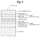
- Fig. 1 is a sectional view showing an example of a configuration of an optical disc according to one embodiment of the invention.
- an optical disc 1 according to this one embodiment has a configuration in which on one main surface of a substrate 2, a reflective layer 3, a lower dielectrics layer 4, a recording layer 5, an upper dielectrics layer 6 and a light transmissive layer 7 are sequentially laminated.
- the optical disc when a track pitch P of a guiding groove, the skew ⁇ of the substrate 2, the numeral aperture NA of an optical pickup that is used to reproduce and/or record an information signal, a wavelength ⁇ of laser light that is used to reproduce and/or record an information signal and a thickness t of the light transmissive layer 7 are made so as to satisfy the following relational equations (1) through (4), a recording capacity of 8 GB or more can be realized.
- the wavelength ⁇ is selected from 400 nm or more and 410 nm or less, the numerical aperture NA from 0.84 or more and 0.86 or less, and a data bit length from 0.1035 ⁇ m or more and 0.12 ⁇ m or less.
- the wavelength ⁇ is selected at 405 nm, the numerical aperture NA at 0.85, the data bit length at 0.12 ⁇ m and the track pitch at 0.32 ⁇ m.
- the numerical aperture NA In the case of the numerical aperture NA being 0.84 or less and the wavelength ⁇ being 410 nm or more, since a spot diameter d (d ⁇ ⁇ /NA) becomes larger than a desired diameter, a high recording density that enables the recording capacity of 8 GB or more cannot be realized.
- the numerical aperture NA In the case of the numerical aperture NA being 0.86 or more and the wavelength ⁇ being 400 nm or less, in order to secure an allowance (tilt margin) of tilt of an optical axis from a recording surface, the light transmissive layer 7 has to be made further thinner; accordingly, an error of a thickness of the light transmissive layer 7 can be confined within an allowable range with difficulty. That is, maintenance of the signal quality becomes difficult.
- the substrate 2 has an annular shape in which a center hole (not shown in the drawing) is formed at a center.
- a pit row for information reproduction or a concaved portion (not shown in the drawing) that becomes a guiding groove for guiding an optical spot when information is recorded or reproduced is formed.
- a thickness of the substrate 2 is selected from 0.3 to 1.2 mm, for instance, at 1.1 mm.
- a plastics material such as a polycarbonate base resin, a polyolefin base resin or an acrylic resin, or glass can be used.
- the plastics material can be preferably used as the material of the substrate 2.
- a material of the reflective layer 3 is selected in view of, for instance, the reflectivity and the thermal conduction of the reflective layer 3. That is, it is selected from metal elements, semi-metal elements and compounds or mixtures thereof that have the reflectivity to a wavelength of laser light that is used for recording and reproducing and the thermal conductivity in the range of, for instance, 4.0 ⁇ 10 -2 to 4. 5 ⁇ 10 2 J/m ⁇ K ⁇ s (4.0 ⁇ 10-4 to 4. 5 J/cm ⁇ K ⁇ s).
- simple bodies such as Al, Ag, Au, Ni, Cr, Ti, Pd, Co, Si, Ta, W, Mo and Ge, or alloys having one of these simple bodies as a main component can be cited.
- Al base, Ag base, Au base, Si base or Ge base materials are preferable.
- AlCu, AlTi, AlCr, AlCo, AlMgSi, AgPdCu, AgPdTi, AgCuTi, AgPdCa, AgPdMg, AgPdFe, Ag and SiB are preferable.
- the reflective layer 3 being constituted of, for instance, a Ag base alloy made of Ag, Nd and Cu, it is preferably selected so that a content of Nd may be in the range of 0.4 atomic percent or more and 0.7 atomic percent or less and that of Cu may be in the range of 0.6 atomic percent or more and 0.9 atomic percent or less.
- a thickness of the reflective layer 3 is preferably selected in the range of 80 nm or more and 140 nm or less, for instance at 100 nm.
- the thickness of the reflective layer 3 is set at less than 80 nm, since heat generated in the recording layer 5 cannot be sufficiently diffused, the thermal cooling becomes insufficient, resulting in deterioration in the jitter characteristics due to a reproduction power at the time of reproduction.
- the thickness of the reflective layer 3 is set at more than 140 nm, although the thermal characteristics and the optical characteristics are not adversely affected, owing to stress generated in the reflective layer 3, the mechanical characteristics such as the skew are adversely affected, resulting in incapability of obtaining desired characteristics.
- the lower dielectrics layer 4 and the upper dielectrics layer 6 are formed by laminating a plurality of dielectrics layers.
- the laminated dielectrics layer is constituted of materials low in the absorptivity to laser light for use in recording and reproducing, preferably of materials extinction coefficient k of which satisfies the relationship of 0 ⁇ k ⁇ 3.
- the lower dielectrics layer 4 is constituted of a first lower dielectrics layer 12 and a second lower dielectrics layer 11 that inhibits a material that constitutes the first lower dielectrics layer from reacting with a material that constitutes the reflective layer 3.
- the upper dielectrics layer 6 is constituted of a first upper dielectrics layer 13 and a second upper dielectrics layer 14 that inhibits a material that constitutes the first upper dielectrics layer 13 from reacting with a material that constitutes the light transmissive layer 7.
- the second lower dielectrics layer 11 and the second upper dielectrics layer 14 are made of Si 3 N 4 .
- the first lower dielectrics layer 12 and the first upper dielectrics layer are made of a mixture of ZnS-SiO 2 , preferably a mixture of ZnS-SiO 2 at a molar ratio of substantially 4: 1.
- a thickness of the second lower dielectrics layer 11 is preferably selected from 8 nm or more and 14 nm or less, for instance, at 10 nm.
- the thickness of the second lower dielectrics layer 4 is set at less than 8 nm, owing to diffusion of Sulfur (S) that constitutes the first lower dielectrics layer 12, the reflective layer 3 is corroded.
- the thickness of the second lower dielectrics layer 4 is set larger than 14 nm, the reflectance decreases and desired signal characteristics becomes incapable of obtaining.
- a thickness of the first lower dielectrics layer 12 is preferably selected from 4 nm or more and 10 nm or less, for instance, at 6 nm.
- the thickness of the first lower dielectrics layer 12 is set at less than 4 nm, it becomes difficult to form the first lower dielectrics layer 12 with a uniform thickness.
- the thickness is set larger than 10 nm, the reflectance decreases and desired signal characteristics becomes incapable of obtaining.
- a thickness of the first upper dielectrics layer 13 is preferably selected from 4 nm or more and 12 nm or less, for instance, at 6 nm.
- the thickness of the first upper dielectrics layer 13 is set at less than 4 nm, it becomes difficult to form the first upper dielectrics layer 13 with a uniform thickness.
- the thickness of the first upper dielectrics layer 13 is set larger than 12 nm, since heat becomes likely to be accumulated in the recording layer 5, resulting in deterioration in the reproduction stability.
- a thickness of the second upper dielectrics layer 14 is preferably selected from 36 nm or more and 46 nm or less, for instance, at 42 nm. When the thickness of the second upper dielectrics layer 14 is selected at less than 36 nm, the reflectance increases, and when it is selected larger than 46 nm, the reflectance decreases.
- the recording layer 5 is a phase change recording layer in which by making use of a crystalline-amorphous structural phase change, an information signal is recorded.
- chalcogen compounds are preferably selected, and more preferably SbTe base alloys are selected.
- SbTe base alloy materials Ge, Sb and Te are preferably selected.
- a content of Ge is selected in the range of 2 atomic percent or more and 8 atomic percent or less
- a ratio of Sb to Te is selected in the range of 3.4 times or more and 4.0 times or less.
- a content of Ge is selected in the range of 2 atomic percent or more and 8 atomic percent or less
- a ratio of Sb to Te is selected in the range of 4.2 times or more and 4.8 times or less.
- a thickness of the recording layer 5 is preferably selected from 6 nm or more and 16 nm or less, for instance, at 10 nm.
- the thickness of the recording layer 5 is selected at less than 6 nm, it becomes difficult to obtain sufficient reproduction durability.
- the thickness is larger than 16 nm, since the recording sensibility becomes poor, an information signal can be recorded with difficulty.
- the light transmissive layer 7 is constituted of a light transmissive sheet (film) having a planar annular shape and an adhesive layer for adhering the light transmissive sheet to the upper dielectrics layer 6 (both are not shown in the drawing).
- the adhesive layer is made of, for instance, a UV-curable resin or a pressure sensitive adhesive (PSA: Pressure Sensitive Adhesive).
- the light transmissive sheet is preferably made of a material that is low in the absorptivity to laser light used for recording/reproducing, specifically, a material having the transmittance of 90 percent or more.
- the light transmissive sheet is made of, for instance, a polycarbonate resin material or a polyolefin base resin.
- a material having the thermal expansion coefficient of substantially 7.0 ⁇ 10 -5 (1/°C) and the bending elasticity of substantially 2.4 ⁇ 10 4 (MPa) is used.
- polyolefin base resin for instance, trademark: Zeonex
- a material having the thermal expansion coefficient of substantially 6.0 ⁇ 10 -5 (1/°C) and the bending elasticity of substantially 2.3 ⁇ 10 4 (MPa) is used.
- a thickness of the light transmissive sheet is selected from a range of 3 ⁇ m to 177 ⁇ m, for instance, at 100 ⁇ m in sum total inclusive a thickness of the adhesive layer.
- the light transmissive sheet according to one of embodiments can be formed, for instance, by inputting a material such as polycarbonate resin in an extruder, followed by melting at a temperature in the range of 250 to 300°C with a heater (not shown in the drawing), further followed by forming into sheet by use of a plurality of cooling rolls, still further followed by cutting in a shape in accordance with the substrate 2.
- a material such as polycarbonate resin
- a heater not shown in the drawing
- a protective layer made of an organic or inorganic material may be further formed.
- a material that hardly has the absorptivity to a wavelength of the laser for use in recording and reproducing is preferable.
- a thickness t of the light transmissive layer 7 is set in the range of 10 to 177 ⁇ m and the dispersion of the thickness of the light transmissive layer is ⁇ t
- a recording capacity can be made 8 GB, and by use of recording and reproducing apparatus similar to existing recording and reproducing apparatus, a higher recording capacity can be attained.
- ⁇ t ⁇ 5.26 ( ⁇ /NA 4 )
- the sputtering device is a leaf type stationary facing sputtering device in which a substrate can rotate on its axis.
- a sputtering device that is used to manufacture an optical disc 1 is shown.
- the sputtering device is constituted by including a vacuum chamber 21 that is a deposition chamber, a vacuum controller 22 that controls a vacuum state in the vacuum chamber 21, a DC high voltage power source 23 for use in plasma discharge, a puttering cathode 25 that is connected through a power source line 24 with the DC high voltage power source 23 for use in plasma discharge, a pallet 26 that is disposed facing the sputtering cathode 25 with a predetermined separation, and a sputter gas supply 27 for supplying a sputter gas such as an inert gas such as Ar or a reaction gas into the vacuum chamber 21.
- a sputter gas such as an inert gas such as Ar or a reaction gas into the vacuum chamber 21.
- the sputtering cathode 25 includes a target 28 that functions as a negative electrode, a backing plate 29 that is constituted so as to fix the target 28 and a magnet system 30 that is disposed on a surface opposite to a surface thereto the target 28 of the backing plate 29 is fixed.
- a pair of electrodes is constituted.
- a substrate 2 on which deposition is performed is attached with a disc base 33 interposed therebetween.
- an inner periphery mask 31 and an outer periphery mask 32 an inner periphery portion and an outer periphery portion of the substrate 2 are covered.
- a substrate rotation driving portion 34 for rotating the pallet 26 in an in-plane direction of the substrate 2 and thereby rotating the substrate 2 is interlockably disposed.
- a substrate 2 that has a planar annular shape as shown in Fig. 4A and on which deposition is performed, and a target 28 that has a disc shape as shown in Fig. 4C and is made of a deposition material, in their planar positional relationship, are disposed so that a center O of the substrate 2 and a center O' of the target 28 may substantially coincide.
- the substrate 2 is constituted so as to be rotated on its axis around the center O owing to the substrate rotation driving portion 34 shown in Fig. 3.
- the sputtering device 20 that is used in the manufacture of an optical disc in one of embodiments is constituted.
- a substrate 2 is carried in a first sputtering device 20 in which a target 28 made of, for instance, AgM (M: additive) is disposed, followed by fastening to a pallet 26.
- a target 28 made of, for instance, AgM (M: additive) is disposed, followed by fastening to a pallet 26.
- the inside of the vacuum chamber 21 is evacuated until a predetermined pressure is attained.
- Ar gas is introduced in the vacuum chamber 21, followed by performing the sputtering, and thereby on one main surface of the substrate 2, a reflective layer 3 made of, for instance, a Ag base alloy is formed.
- the substrate 2 is carried in a second sputtering device 20 that is provided with, for instance, a Si target, followed by fastening to the pallet 26. Then, the inside of the vacuum chamber 21 is evacuated until a predetermined pressure is attained. In the next place, for instance, Ar gas and nitrogen are introduced in the vacuum chamber 21, followed by carrying out the sputtering, and thereby on the reflective layer 3, a second lower dielectrics layer 11 made of, for instance, Si 3 N 4 is formed.
- a second sputtering device 20 that is provided with, for instance, a Si target, followed by fastening to the pallet 26. Then, the inside of the vacuum chamber 21 is evacuated until a predetermined pressure is attained. In the next place, for instance, Ar gas and nitrogen are introduced in the vacuum chamber 21, followed by carrying out the sputtering, and thereby on the reflective layer 3, a second lower dielectrics layer 11 made of, for instance, Si 3 N 4 is formed.
- the substrate 2 is carried in a third sputtering device 20 provided with a target 28 made of, for instance, a ZnS-SiO 2 mixture, followed by fastening to the pallet 26.
- a target 28 made of, for instance, a ZnS-SiO 2 mixture
- the inside of the vacuum chamber 21 is evacuated until a predetermined pressure is attained.
- an inert gas such as Ar gas is introduced in the vacuum chamber 21, followed by carrying out the sputtering, and thereby on the second lower dielectrics layer 11, a first lower dielectrics layer 12 made of, for instance, a ZnS-SiO 2 mixture is formed.
- the substrate 2 is carried in a fourth sputtering device 20 provided with a target 28 made of, for instance, a GeSbTe alloy, followed by fastening to the pallet 26. Then the inside of the vacuum chamber 21 is evacuated until a predetermined pressure is attained. Thereafter, an inert gas such as Ar gas is introduced in the vacuum chamber 21, followed by carrying out the sputtering, and thereby on the first lower dielectrics layer 12, a recording layer 5 made of, for instance, a GeSbTe alloy is formed.
- a target 28 made of, for instance, a GeSbTe alloy
- the substrate 2 is carried in a fifth sputtering device 20 provided with a target 28 made of, for instance, a ZnS-SiO 2 mixture, followed by fastening to the pallet 26. Then the inside of the vacuum chamber 21 is evacuated until a predetermined pressure is attained. Thereafter, an inert gas such as Ar gas is introduced in the vacuum chamber 21, followed by carrying out the sputtering, and thereby on the recording layer 5, a first upper dielectrics layer 13 made of, for instance, a ZnS-SiO 2 mixture is formed.
- a target 28 made of, for instance, a ZnS-SiO 2 mixture
- the substrate 2 on which a first upper dielectrics layer 13 is formed is carried in a sixth sputtering device provided with a target made of, for instance, Si, followed by fastening to the pallet 26. Then the inside of the vacuum chamber 21 is evacuated until a predetermined pressure is attained. In the next place, for instance Ar gas and nitrogen are introduced in the vacuum chamber 21, followed by carrying out the sputtering, and thereby on one main surface of the substrate 2, a second upper dielectrics layer 14 made of, for instance, Si 3 N 4 is formed on the first upper dielectrics layer 13.
- the substrate 2 is carried in a predetermined position of a laminator (omitted from showing in the drawing). Subsequently, a planar annular light transmissive sheet, with a pressure sensitive adhesive (PSA) previously uniformly coated on one main surface of the sheet, is adhered on a side where the respective layers are formed on the substrate 2. Thereby, the light transmissive layer 7 is formed so as to cover the respective layers formed on the substrate 2.
- PSA pressure sensitive adhesive
- an optical disc 1 shown in Fig. 1 is manufactured. After the optical disc 1 is thus manufactured, a state of the recording layer 5 is preferably made crystalline by use of an initializing device.
- a material that constitutes a first lower dielectrics layer 12 and a material that constitutes a reflective layer 3 can be inhibited from reacting and a material that constitutes a first upper dielectrics layer 13 and a material that constitutes a light transmissive layer 7 can be inhibited from reacting. Accordingly, an optical disc can be inhibited from corroding and excellent signal characteristics can be obtained.
- a recording layer 5 being formed of a SbTe base alloy material made of Ge, Sb and Te
- a content of Ge is selected at 2 atomic percent or more and 8 atomic percent or less, and a ratio of Sb to Te is selected at 3.4 times or more and 4.0 times or less
- an information signal being recorded at a line speed selected from a range of 4.554 m/s or more and 5.28 m/s or less
- the jitter value and the recording sensitivity can be improved, and excellent signal characteristics can be obtained.
- the recording layer 5 being formed of a SbTe base alloy made of Ge, Sb and Te
- a content of Ge is selected at 2 atomic percent or more and 8 atomic percent or less, and a ratio of Sb to Te is selected at 4.2 times or more and 4.8 times or less, even in the case of, with a line speed selected from a range of 4.554 m/s or more and 5.28 m/s or less as a reference, an information signal being recorded at a line speed two times thereof, the jitter value and the recording sensitivity can be improved, and excellent signal characteristics can be obtained.
- Examples 1 through 4 relates to optical discs formed by laminating, on a substrate 2, a reflective layer 3 made of AgNdCu, a second lower dielectrics layer 11 made of Si 3 N 4 , a first lower dielectrics layer 12 made of a ZnS-SiO 2 mixture, a recording layer 5 made of GeSbTe, a first upper dielectrics layer 13 made of a ZnS-SiO 2 mixture, a second upper dielectrics layer 14 made of Si 3 N 4 , and a light transmissive layer 7.
- the substrate 2 has a diameter of 120 mm and a thickness of 1.1 mm.
- the light transmissive layer 7 is formed by laminating a light transmissive sheet having a planar annular shape through an adhesive layer made of a pressure sensitive adhesive (PSA) coated previously uniformly on one main surface of the light transmissive sheet onto a upper dielectrics layer 6.
- PSA pressure sensitive adhesive
- Examples 1 through 4 relate to optical discs that are different from each other in thickness of the reflective layer 3, and the thicknesses thereof are, in turn of examples 1 through 4, 60 nm, 80 nm, 120 nm and 140 nm.
- thicknesses of the respective layers other than the reflective layer 3 are the same and the second lower dielectrics layer 11, the first lower dielectrics layer 12, the recording layer 5, the first upper dielectrics layer 13 and the second upper dielectrics layer 14, respectively, are 8 nm, 6 nm, 10 nm, 8 nm and 40 nm in the thickness.
- the deposition conditions of the reflective layer 3, the first lower dielectrics layer 12, the recording layer 5 and the first upper dielectrics layer 13 are as follows.
- the deposition conditions of the second lower dielectrics layer 11 and the second upper dielectrics layer 14 are as follows.
- a thickness of the reflective layer 3 was determined by properly adjusting a time based on a calibration curve obtained from relationship between a deposition time and a film thickness.
- Examples 5 through 8 relate to optical discs that are different from each other in thickness of the second lower dielectrics layer 11, and the thicknesses thereof are, in turn of examples 5 through 8, 4 nm, 8 nm, 14 nm and 18 nm.
- thicknesses of the respective layers other than the second lower dielectrics layer 11 are the same, and the reflective layer 3, the first lower dielectrics layer 12, the recording layer 5, the first upper dielectrics layer 13 and the second upper dielectrics layer 14, respectively, are 100 nm, 6 nm, 10 nm, 8 nm and 40 nm in the thickness.
- a thickness of the second lower dielectrics layer 11 was determined by properly adjusting a time based on a calibration curve obtained from relationship between a deposition time and a film thickness. Other than these are similar to examples 1 through 4.
- Examples 9 through 11 relate to optical discs that are different in thickness of the first lower dielectrics layer 12 from each other, and the thicknesses thereof are, in turn of examples 9 through 11, respectively, 4 nm, 10 nm and 12 nm.
- thicknesses of the respective layers other than the first lower dielectrics layer 12 are the same, and the reflective layer 3, the second lower dielectrics layer 11, the recording layer 5, the first upper dielectrics layer 13 and the second upper dielectrics layer 14, respectively, are 100 nm, 8 nm, 10 nm, 8 nm and 40 nm in the thickness.
- a thickness of the first lower dielectrics layer 12 was determined by properly adjusting a time based on a calibration curve obtained from relationship between a deposition time and a film thickness. Other than these are similar to examples 1 through 4.
- Examples 12 through 15 relate to optical discs that are different from each other in the thickness of the recording layer 5, and the thicknesses thereof are, in turn of examples 12 through 15, 6 nm, 8 nm, 16 nm and 18 nm.
- thicknesses of the respective layers other than the recording layer 5 are the same; that is, the reflective layer 3, the second lower dielectrics layer 11, the first lower dielectrics layer 12, the first upper dielectrics layer 13 and the second upper dielectrics layer 14, respectively, are 100 nm, 8 nm, 6 nm, 8 nm and 40 nm in the thickness.
- a thickness of the recording layer 5 was determined by properly adjusting a time based on a calibration curve obtained from relationship between a deposition time and a film thickness. Other than these are similar to examples 1 through 4.
- Examples 16 through 18 relate to optical discs that are different from each other in thickness of the first upper dielectrics layer 13, and the thicknesses thereof are, in turn of examples 16 through 18, 4 nm, 10 nm and 12 nm.
- thicknesses of the respective layers other than the first upper dielectrics layer 13 are the same; that is, the reflective layer 3, the second lower dielectrics layer 11, the first lower dielectrics layer 12, the recording layer 5 and the second upper dielectrics layer 14, respectively, are 100 nm, 8 nm, 6 nm, 10 nm and 40 nm in the thickness.
- a thickness of the first upper dielectrics layer 13 was determined by properly adjusting a time based on a calibration curve obtained from relationship between a deposition time and a film thickness. Other than these are similar to examples 1 through 4.
- Examples 19 through 22 relate to optical discs that are different from each other in thickness of the second upper dielectrics layer 14, and the thicknesses thereof are, in turn of examples 19 through 22, 30 nm, 36 nm, 46 nm and 50 nm.
- thicknesses of the respective layers other than the second upper dielectrics layer 14 are the same; that is, the reflective layer 3, the second lower dielectrics layer 11, the first lower dielectrics layer 12, the recording layer 5 and the first upper dielectrics layer 13, respectively, are 100 nm, 8 nm, 6 nm, 10 nm and 8 nm in the thickness.
- a thickness of the second upper dielectrics layer 14 was determined by properly adjusting a time based on a calibration curve obtained from relationship between a deposition time and a film thickness. Other than these are similar to examples 1 through 4.
- a comparative example relates to an optical disc that has a configuration in which the first lower dielectrics layer 12 and the first upper dielectrics layer 13 in example 1 are omitted.
- the reflective layer 3, the second lower dielectrics layer 11, the recording layer 5 and the second upper dielectrics layer 14, respectively, are 100 nm, 18 nm, 10 nm and 50 nm in thickness. Other than these are similar to example 1.
- a content of Nd in the reflective layer 3 is 0.4 atomic percent and that of Cu is 0.6 atomic percent.
- a content of Nd in the reflective layer 3 is 0.7 atomic percent and that of Cu is 0.9 atomic percent.
- thicknesses of the reflective layer 3, the second lower dielectrics layer 11, the first lower dielectrics layer 12, the recording layer 5, the first upper dielectrics layer 13 and the second upper dielectrics layer 14, respectively, are 100 nm, 8 nm, 6 nm, 10 nm, 8 nm and 40 nm. Other than these are similar to examples 1 through 4.
- Ratios of Sb to Te contained in the recording layers 5 of optical discs according to examples 25 through 30 are, respectively, in turn of examples 25 through 30, 3.2, 3.4, 3.7, 4, 4.4 and 4.7.
- a content of Ge contained in the recording layers 5 of the optical discs according to examples 25 through 30 is 4 atomic percent.
- film thicknesses of the reflective layer 3, the second lower dielectrics layer 11, the first lower dielectrics layer 12, the recording layer 5, the first upper dielectrics layer 13 and the second upper dielectrics layer 14, respectively, are 100 nm, 10 nm, 5 nm, 12 nm, 6 nm and 42 nm. Other than these are similar to examples 1 through 4.
- Contents of Ge contained in the recording layers 5 of optical discs according to examples 31 through 34, respectively, are in turn of examples 31 through 34, 0, 2, 8 and 10 atomic percent.
- a ratio of Sb to Te contained in the recording layers 5 of examples 31 through 34 is 3.6.
- film thicknesses of the reflective layer 3, the second lower dielectrics layer 11, the first lower dielectrics layer 12, the recording layer 5, the first upper dielectrics layer 13 and the second upper dielectrics layer 14, respectively are 100 nm, 10 nm, 5 nm, 12 nm, 6 nm and 42 nm. Other than these are similar to examples 1 through 4.
- Ratios of Sb to Te contained in the recording layers 5 of optical discs according to examples 35 through 40 are, respectively, in turn of examples 35 through 40, 3.7, 4, 4.2, 4.4, 4.8 and 5.
- a content of Ge contained in the recording layers 5 of examples 35 through 40 is 4 atomic percent.
- film thicknesses of the reflective layer 3, the second lower dielectrics layer 11, the first lower dielectrics layer 12, the recording layer 5, the first upper dielectrics layer 13 and the second upper dielectrics layer 14, respectively are 100 nm, 8 nm, 6 nm, 10 nm, 8 nm and 40 nm. Other than these are similar to examples 1 through 4.
- Contents of Ge contained in the recording layers 5 of optical discs according to examples 41 through 44, respectively, in turn of examples 41 through 44, are 0, 2, 8 and 10 atomic percent.
- a ratio of Sb to Te contained in the recording layers 5 of examples 41 through 44 is 4.2.
- film thicknesses of the reflective layer 3, the second lower dielectrics layer 11, the first lower dielectrics layer 12, the recording layer 5, the first upper dielectrics layer 13 and the second upper dielectrics layer 14, respectively are 100 nm, 8 nm, 6 nm, 10 nm, 8 nm and 40 nm. Other than these are similar to examples 1 through 4.
- the present inventors as shown in Fig. 7, recorded an information signal at a line speed of 5.28 m/s (1 ⁇ ) to the abovementioned optical discs according to examples 1 through 24 and comparative example and thereby evaluated the reflectance of groove, the modulation factor, the recording sensitivity, the reproduction durability, and the corrosion resistance. Furthermore, to that according to the examples 1 through 24 and comparative example, an information signal was recorded at 10.56 m/s (2 ⁇ ), and the modulation factor and the recording sensitivity were evaluated. At the recording of an information signal, states of the recording layers 5 of optical discs according to examples 1 through 24 and comparative example were made crystalline by use of an initialization device.
- a recording emission pattern used at the evaluation of the optical discs according to examples 1 through 24 and comparative example is shown.
- the respective conditions at the time of recording of an information signal other than the line speed are shown below.
- Optical discs according to examples 1 through 24 and comparative example were held under an environment where a temperature is 80°C and the humidity is 85 percent for 400 hours. Thereafter, whether the corrosion was generated or not was judged of the optical discs according to examples 1 through 24 and comparative example. In Fig. 7, an optical disc where the corrosion was not generated is expressed with [ ⁇ ] and an optical disc where the corrosion was generated is expressed with [ ⁇ ].
- the thickness of the reflective layer 3 is 80 nm or more and 140 nm or less
- the thickness of the second lower dielectrics layer 11 is 8 nm or more and 14 nm or less
- the thickness of the first lower dielectrics layer 12 is 4 nm or more and 10 nm or less
- the thickness of the recording layer 5 is 8 nm or more and 16 nm or less
- the thickness of the first upper dielectrics layer 13 is 4 nm or more and 12 nm or less
- the thickness of the second upper dielectrics layer 14 is 36 nm or more and 46 nm or less
- the present inventors measured and evaluated the overwrite (DOW: Direct Over-Write) recording characteristics of optical discs according to examples 1 through 24 and comparative example.
- DOW Direct Over-Write
- Fig. 11 the overwrite recording characteristics in example 23 and a comparative example are shown. From Fig. 11, it can be confirmed that, in example 23, in comparison with the comparative example, the overwrite characteristics and the bottom jitter characteristics are largely improved.
- the present inventors measured the recording characteristics including the crosswrite of optical discs according to examples 1 through 24 and a comparative example. In what follows, for convenience sake, measurements of the recording characteristics including the crosswrite of example 23 and a comparative example will be shown.
- Fig. 12 the recording characteristics including the crosswrite of example 23 are shown. From Fig. 12, it is found that at both line speeds of 5.28 m/s (1 ⁇ ) and 10.56 m/s (2 ⁇ ), excellent jitter characteristics and recording sensitivity can be obtained.
- the present inventors recorded an information signal at a line speed of 5.28 m/s (1 ⁇ ) on the optical discs according to examples 25 through 34 and evaluated the jitter value, the recording sensitivity and the storage characteristics.
- a recording light-emission pattern that is used in the evaluation and the respective conditions at the time of recording an information signal are similar to that used at the time of evaluation of examples 1 through 24.
- the jitter value In the case of the jitter value being smaller than 9 percent, the jitter value was judged excellent, and in the case of the jitter value being 9 percent or more, it was judged poor.
- Fig. 8 an example where the jitter value was excellent is expressed with [ ⁇ ] and an example where the jitter value was poor is expressed with [ ⁇ ].
- the jitter values were measured. In the case of the jitter value being smaller than 9 percent, the jitter value was judged excellent, and in the case of the jitter value being 9 percent or more, it was judged poor. In Fig. 8, an example where the jitter value was excellent is expressed with [ ⁇ ] and an example where the jitter value was bad is expressed with [ ⁇ ].
- the recording layer being made of Ge, Sb and Te, with a content of Ge selected at 2 atomic percent or more and 8 atomic percent or less and a ratio of Sb to Te selected at 3.4 times or more and 4.0 times or less, when an information signal is recorded under the conditions where the line speed is 5.28 m/s (1 ⁇ ), the laser wavelength is 405 nm, the NA is 0.85 and the data bit length is 0.12 ⁇ m, excellent jitter value, recording sensitivity and storage characteristics can be obtained.
- the present inventors recorded an information signal at line speeds of 5.28 m/s (1 ⁇ ) and 10.56 m/s (2 ⁇ ) on the optical discs according to examples 35 through 44 and evaluated the jitter value, the recording sensitivity and the storage characteristics.
- a recording light-emission pattern that is used in the evaluation and the respective conditions at the time of recording an information signal are similar to that used at the time of evaluation of examples 1 through 24.
- the jitter value In the case of the jitter value being smaller than 12.5 percent, the jitter value was judged excellent, and in the case of the jitter value being 12.5 percent or more, it was judged poor.
- Fig. 9 an example where the jitter value was excellent is expressed with [ ⁇ ] and an example where the jitter value was poor is expressed with [ ⁇ ].
- the jitter values were measured. In the case of the jitter value being smaller than 12.5 percent, the jitter value was judged excellent, and in the case of the jitter value being 12.5 percent or more, it was judged poor. In Fig. 9, an example where the jitter value was excellent is expressed with [ ⁇ ] and an example where the jitter value was poor is expressed with [ ⁇ ].
- a multi-layered film is laminated on a light transmissive layer on which a guide groove is formed and lastly a smooth supporting substrate may be formed.
- a method of forming a concaved groove track on the light transmissive layer for instance, an injection molding method, a photopolymer method (2P method: Photo Polymerization), a method of transcribing a concaved pattern due to the pressure bonding and pressurization can be used.
- a method of manufacturing optical discs according to one of abovementioned embodiments is preferably used.
- a case where a light transmissive sheet is laminated through a pressure sensitive adhesive previously uniformly coated on one main surface of the light transmissive sheet on a substrate 2, and thereby a light transmissive layer 7 is formed is shown as an example.
- a method of manufacturing the light transmissive layer 7 is not restricted thereto.
- a UV-curable resin is coated between one main surface of a light transmissive sheet and a second upper dielectrics layer 6 followed by curing by irradiating UV, and thereby a light transmissive layer 7 may be formed.
- a leaf type stationary facing sputtering device in which one target is opposed to one disc substrate, planar positional relationship therebetween is set as shown in Fig. 4.
- the invention is not necessarily restricted to the leaf type stationary facing sputtering device.
- a sputtering device in which as shown in Fig. 13A a plurality of substrates 2 (8 pieces in Fig. 13A) is fastened to a pallet 26, as shown in Fig. 13B a plurality of targets 28 is fastened to a vacuum chamber 21, and in positional relationship shown in Fig. 13C, with the pallet 26 rotating in a direction of an arrow mark b, deposition is carried out to a plurality of substrates 2 can be applied.
- a material that constitutes a first lower dielectrics layer and a material that constitutes a reflective layer can be inhibited from reacting, and a material that constitutes a first upper dielectrics layer and a material that constitutes a light transmissive layer can be inhibited from reacting; accordingly, excellent signal characteristics and high reliability can be obtained.
Abstract
Description
wherein light having a wavelength in a range of 400 nm or more and 410 nm or less is focused with an optical system having a numeral aperture in the range of 0.84 or more and 0.86 or less followed by irradiating from a side of the light transmissive layer on the recording layer, and thereby a information signal is recorded and reproduced,
wherein the lower dielectrics layer includes a first lower dielectric layer and a second lower dielectrics layer that inhibits a material that constitutes the first lower dielectrics layer and a material that constitutes the reflective layer from reacting; and
the upper dielectrics layer includes a first upper dielectric layer and a second upper dielectrics layer that inhibits a material that constitutes the first upper dielectrics layer and a material that constitutes the light transmissive layer from reacting.
wherein light having a wavelength in the range of 400 nm or more and 410 nm or less is focused with an optical system having a numeral aperture in the range of 0.84 or more and 0.86 or less followed by irradiating from a side of the light transmissive layer on the recording layer, and thereby a information signal is recorded and reproduced, comprising:
Claims (26)
- An optical recording medium comprising at least a reflective layer, a lower dielectrics layer, a recording layer, an upper dielectrics layer and a light transmissive layer that are sequentially laminated on one main surface of a substrate,
wherein light having a wavelength in the range of 400 nm or more and 410 nm or less is focused with an optical system having a numeral aperture in the range of 0.84 or more and 0.86 or less followed by irradiating from a side of the light transmissive layer on the recording layer, and thereby an information signal is recorded and reproduced,
wherein the lower dielectrics layer includes a first lower dielectrics layer and a second lower dielectrics layer that inhibits a material that constitutes the first lower dielectrics layer and a material that constitutes the reflective layer from reacting; and
the upper dielectrics layer includes a first upper dielectrics layer and a second upper dielectrics layer that inhibits a material that constitutes the first upper dielectrics layer and a material that constitutes the light transmissive layer from reacting. - The optical recording medium according to claim 1,
wherein extinction coefficients k of materials that constitute the upper dielectrics layer and the lower dielectrics layer satisfy relationship of 0 < k ≤ 3. - The optical recording medium according to claim 1,
wherein the first lower dielectrics layer is made of a mixture of zinc sulfide and silicon oxide and the second lower dielectrics layer is made of silicon nitride. - The optical recording medium according to claim 1,
wherein the first upper dielectrics layer is made of a mixture of zinc sulfide and silicon oxide and the second upper dielectrics layer is made of silicon nitride. - The optical recording medium according to claim 1,
wherein the recording layer is a phase change recording layer. - The optical recording medium according to claim 5,
wherein the phase change recording layer is made of a SbTe base alloy, and the reflective layer is made of a Ag base alloy. - The optical recording medium according to claim 6,
wherein the SbTe base alloy includes Ge, Sb and Te, and the Ag base alloy includes Ag, Nd and Cu. - The optical recording medium according to claim 7,
wherein in the phase change recording layer, a content of Ge is 2 atomic percent or more and 8 atomic percent or less, and a ratio of Sb to Te is 3.4 times or more and 4.0 times or less, and
in the reflective layer a content of Nd is 0.4 atomic percent or more and 0.7 atomic percent or less and a content of Cu is 0.6 atomic percent or more and 0.9 atomic percent or less. - The optical recording medium according to claim 7,
wherein in the phase change recording layer, a content of Ge is 2 atomic percent or more and 8 atomic percent or less, and a ratio of Sb to Te is 4.2 times or more and 4.8 times or less, and
in the reflective layer a content of Nd is 0.4 atomic percent or more and 0.7 atomic percent or less and a content of Cu is 0.6 atomic percent or more and 0.9 atomic percent or less. - The optical recording medium according to claim 1,
wherein a thickness of the reflective layer is 80 nm or more and 140 nm or less;
a thickness of the second lower dielectrics layer is 8 nm or more and 14 nm or less;
a thickness of the first lower dielectrics layer is 4 nm or more and 10 nm or less;
a thickness of the recording layer is 8 nm or more and 16 nm or less;
a thickness of the first upper dielectrics layer is 4 nm or more and 12 nm or less; and
a thickness of the second upper dielectrics layer is 36 nm or more and 46 nm or less. - The optical recording medium according to claim 1,
wherein the light transmissive layer includes a light transmissive sheet and an adhesive layer for adhering the light transmissive sheet to a substrate. - The optical recording medium according to claim 11,
wherein the adhesive layer is made of a pressure sensitive adhesive. - The optical recording medium according to claim 11,
wherein the adhesive layer is made of a UV-curable resin. - A method of manufacturing an optical recording medium that comprises at least a reflective layer, a lower dielectrics layer, a recording layer, an upper dielectrics layer and a light transmissive layer that are sequentially laminated on one main surface of a substrate,
wherein light having a wavelength in the range of 400 nm or more and 410 nm or less is focused with an optical system having a numeral aperture in the range of 0.84 or more and 0.86 or less followed by irradiating from a side of the light transmissive layer on the recording layer, and thereby an information signal is recorded and reproduced, comprising:forming the reflective layer on one main surface of a substrate;a first lower dielectrics layer and a second lower dielectrics layer that inhibits a material that constitutes the first lower dielectrics layer and a material that constitutes the reflective layer from reacting, and thereby forming the lower dielectrics layer;forming the recording layer on the lower dielectrics layer;a first upper dielectrics layer and a second upper dielectrics layer that inhibits a material that constitutes the first upper dielectrics layer and a material that constitutes the light transmissive layer from reacting, and thereby forming the upper dielectrics layer; andforming the light transmissive layer on the upper dielectrics layer. - The method of manufacturing an optical recording medium according to claim 14, wherein extinction coefficients k of materials that constitute the upper dielectrics layer and the lower dielectrics layer satisfy relationship of 0 < k ≤ 3.
- The method of manufacturing an optical recording medium according to claim 14, wherein the first lower dielectrics layer is made of a mixture of zinc sulfide and silicon oxide and the second lower dielectrics layer is made of silicon nitride.
- The method of manufacturing an optical recording medium according to claim 14, wherein the first upper dielectrics layer is made of a mixture of zinc sulfide and silicon oxide and the second upper dielectrics layer is made of silicon nitride.
- The method of manufacturing an optical recording medium according to claim 14, wherein the recording layer is a phase change recording layer.
- The method of manufacturing an optical recording medium according to claim 18, wherein the phase change recording layer is made of a SbTe base alloy, and the reflective layer is made of a Ag base alloy.
- The method of manufacturing an optical recording medium according to claim 19, wherein the SbTe base alloy includes Ge, Sb and Te, and the Ag base alloy includes Ag, Nd and Cu.
- The method of manufacturing an optical recording medium according to claim 20, wherein in the phase change recording layer, a content of Ge is 2 atomic percent or more and 8 atomic percent or less, and a ratio of Sb to Te is 3.4 times or more and 4.0 times or less, and
in the reflective layer a content of Nd is 0.4 atomic percent or more and 0.7 atomic percent or less and a content of Cu is 0.6 atomic percent or more and 0.9 atomic percent or less. - The method of manufacturing an optical recording medium according to claim 20, wherein in the phase change recording layer, a content of Ge is 2 atomic percent or more and 8 atomic percent or less, and a ratio of Sb to Te is 4.2 times or more and 4.8 times or less, and
in the reflective layer a content of Nd is 0.4 atomic percent or more and 0.7 atomic percent or less and a content of Cu is 0.6 atomic percent or more and 0.9 atomic percent or less. - The method of manufacturing an optical recording medium according to claim 14, wherein a thickness of the reflective layer is 80 nm or more and 140 nm or less;
a thickness of the second lower dielectrics layer is 8 nm or more and 14 nm or less;
a thickness of the first lower dielectrics layer is 4 nm or more and 10 nm or less;
a thickness of the recording layer is 8 nm or more and 16 nm or less;
a thickness of the first upper dielectrics layer is 4 nm or more and 12 nm or less; and
a thickness of the second upper dielectrics layer is 36 nm or more and 46 nm or less. - The method of manufacturing an optical recording medium according to claim 14, wherein the light transmissive layer is formed by adhering a light transmissive sheet to the upper dielectrics layer with an adhesive layer.
- The method of manufacturing an optical recording medium according to claim 24, wherein the adhesive layer is made of a pressure sensitive adhesive.
- The method of manufacturing an optical recording medium according to claim 24, wherein the adhesive layer is made of a UV-curable resin.
Applications Claiming Priority (3)
| Application Number | Priority Date | Filing Date | Title |
|---|---|---|---|
| JP2003030114 | 2003-02-06 | ||
| JP2003030114A JP4667721B2 (en) | 2003-02-06 | 2003-02-06 | Optical recording medium and manufacturing method thereof |
| PCT/JP2004/000536 WO2004070717A1 (en) | 2003-02-06 | 2004-01-22 | Optical recording medium and method for manufacturing same |
Publications (3)
| Publication Number | Publication Date |
|---|---|
| EP1592003A1 true EP1592003A1 (en) | 2005-11-02 |
| EP1592003A4 EP1592003A4 (en) | 2006-02-08 |
| EP1592003B1 EP1592003B1 (en) | 2007-02-28 |
Family
ID=32844259
Family Applications (1)
| Application Number | Title | Priority Date | Filing Date |
|---|---|---|---|
| EP04704344A Expired - Fee Related EP1592003B1 (en) | 2003-02-06 | 2004-01-22 | Optical recording medium and method for manufacturing same |
Country Status (8)
| Country | Link |
|---|---|
| US (1) | US7787353B2 (en) |
| EP (1) | EP1592003B1 (en) |
| JP (1) | JP4667721B2 (en) |
| KR (1) | KR101017004B1 (en) |
| CN (2) | CN100372009C (en) |
| DE (1) | DE602004005007T2 (en) |
| TW (1) | TW200426816A (en) |
| WO (1) | WO2004070717A1 (en) |
Families Citing this family (5)
| Publication number | Priority date | Publication date | Assignee | Title |
|---|---|---|---|---|
| US7378953B2 (en) * | 2004-08-30 | 2008-05-27 | International Business Machines Corporation | Transmission between a sensor and a controller in a wireless sensor network |
| JP4592388B2 (en) * | 2004-11-04 | 2010-12-01 | シャープ株式会社 | III-V compound semiconductor light emitting device and method for manufacturing the same |
| KR100747577B1 (en) * | 2005-12-28 | 2007-08-08 | 엘지전자 주식회사 | High definition optical media |
| JP2007299472A (en) * | 2006-04-28 | 2007-11-15 | Fujitsu Ltd | Optical reproduction medium, and manufacturing method of optical reproduction medium |
| CN109799014A (en) * | 2019-03-01 | 2019-05-24 | 西安交通大学 | A kind of flexible pressure-sensitive sensor and preparation method thereof |
Citations (4)
| Publication number | Priority date | Publication date | Assignee | Title |
|---|---|---|---|---|
| US6096399A (en) * | 1997-12-22 | 2000-08-01 | Tdk Corporation | Optical recording medium |
| WO2002076757A1 (en) * | 2001-03-23 | 2002-10-03 | Sony Corporation | Multi-layered optical disc |
| US20020150772A1 (en) * | 2000-12-26 | 2002-10-17 | Kabushiki Kaisha Kobe Seiko Sho (Kobe Steel, Ltd.) | Reflection layer or semi-transparent reflection layer for use in optical information recording media, optical information recording media and sputtering target for use in the optical information recording media |
| JP2003006930A (en) * | 2001-06-18 | 2003-01-10 | Sony Corp | Optical recording medium |
Family Cites Families (23)
| Publication number | Priority date | Publication date | Assignee | Title |
|---|---|---|---|---|
| US6218292B1 (en) * | 1997-12-18 | 2001-04-17 | Advanced Micro Devices, Inc. | Dual layer bottom anti-reflective coating |
| JP3698905B2 (en) * | 1999-01-11 | 2005-09-21 | 日本電気株式会社 | Optical information recording medium, information recording method thereof, and information erasing method thereof |
| KR20010075534A (en) * | 1999-08-31 | 2001-08-09 | 니시무로 타이죠 | Optical disk, and method and apparatus for reading data from optical disk |
| US6469977B2 (en) * | 1999-12-20 | 2002-10-22 | Matsushita Electric Industrial Co., Ltd. | Optical information recording medium, method for producing the same, and method and apparatus for recording/reproducing information thereon |
| JP3365762B2 (en) * | 2000-04-28 | 2003-01-14 | 株式会社神戸製鋼所 | Reflective layer or translucent reflective layer for optical information recording medium, optical information recording medium, and sputtering target for optical information recording medium |
| JP4046955B2 (en) | 2000-06-16 | 2008-02-13 | 三菱化学メディア株式会社 | Optical information recording medium |
| JP3593003B2 (en) | 2000-06-23 | 2004-11-24 | 三菱化学株式会社 | Optical information recording medium |
| JP2002022570A (en) * | 2000-07-05 | 2002-01-23 | Showa Corp | Torque sensor |
| TW575873B (en) * | 2000-07-13 | 2004-02-11 | Matsushita Electric Ind Co Ltd | Information recording medium, method for producing the same, and recording/reproducing method using the same |
| JP4509431B2 (en) | 2000-07-13 | 2010-07-21 | パナソニック株式会社 | Information recording medium |
| JP2002074746A (en) * | 2000-09-01 | 2002-03-15 | Matsushita Electric Ind Co Ltd | Optical information recording medium |
| JP2002074747A (en) | 2000-09-01 | 2002-03-15 | Ricoh Co Ltd | Optical recording medium |
| EP1229530A3 (en) * | 2001-02-01 | 2006-10-18 | Ricoh Company, Ltd. | Optical information recording medium |
| JP2002237088A (en) | 2001-02-09 | 2002-08-23 | Ricoh Co Ltd | Optical information recording medium and method for recording onto the medium |
| JP4141652B2 (en) * | 2001-03-05 | 2008-08-27 | 株式会社リコー | Phase change optical recording medium |
| JP2002269812A (en) | 2001-03-14 | 2002-09-20 | Sony Corp | Optical recording medium and method for manufacturing the same |
| JP2003019867A (en) | 2001-04-19 | 2003-01-21 | Mitsubishi Chemicals Corp | Optical recording medium |
| JP2002324335A (en) | 2001-04-26 | 2002-11-08 | Sony Corp | Optical recording medium and its manufacturing method |
| JP4239428B2 (en) * | 2001-04-27 | 2009-03-18 | ソニー株式会社 | Optical recording medium |
| JP2003022570A (en) * | 2001-07-10 | 2003-01-24 | Ricoh Co Ltd | Optical recording medium and manufacturing method therefor |
| TWI234157B (en) * | 2001-12-07 | 2005-06-11 | Matsushita Electric Ind Co Ltd | Information recording medium and method for producing the same |
| KR20030065959A (en) * | 2002-02-02 | 2003-08-09 | 삼성전자주식회사 | High density optical disk |
| JP2004095034A (en) * | 2002-08-30 | 2004-03-25 | Pioneer Electronic Corp | Information recording medium |
-
2003
- 2003-02-06 JP JP2003030114A patent/JP4667721B2/en not_active Expired - Lifetime
-
2004
- 2004-01-22 CN CNB2004800002656A patent/CN100372009C/en not_active Expired - Fee Related
- 2004-01-22 KR KR1020047015926A patent/KR101017004B1/en not_active IP Right Cessation
- 2004-01-22 EP EP04704344A patent/EP1592003B1/en not_active Expired - Fee Related
- 2004-01-22 US US10/509,308 patent/US7787353B2/en active Active
- 2004-01-22 WO PCT/JP2004/000536 patent/WO2004070717A1/en active IP Right Grant
- 2004-01-22 DE DE602004005007T patent/DE602004005007T2/en not_active Expired - Lifetime
- 2004-01-22 CN CN2007101283703A patent/CN101101773B/en not_active Expired - Lifetime
- 2004-02-03 TW TW093102391A patent/TW200426816A/en unknown
Patent Citations (4)
| Publication number | Priority date | Publication date | Assignee | Title |
|---|---|---|---|---|
| US6096399A (en) * | 1997-12-22 | 2000-08-01 | Tdk Corporation | Optical recording medium |
| US20020150772A1 (en) * | 2000-12-26 | 2002-10-17 | Kabushiki Kaisha Kobe Seiko Sho (Kobe Steel, Ltd.) | Reflection layer or semi-transparent reflection layer for use in optical information recording media, optical information recording media and sputtering target for use in the optical information recording media |
| WO2002076757A1 (en) * | 2001-03-23 | 2002-10-03 | Sony Corporation | Multi-layered optical disc |
| JP2003006930A (en) * | 2001-06-18 | 2003-01-10 | Sony Corp | Optical recording medium |
Non-Patent Citations (2)
| Title |
|---|
| PATENT ABSTRACTS OF JAPAN vol. 2003, no. 05, 12 May 2003 (2003-05-12) & JP 2003 006930 A (SONY CORP), 10 January 2003 (2003-01-10) * |
| See also references of WO2004070717A1 * |
Also Published As
| Publication number | Publication date |
|---|---|
| DE602004005007T2 (en) | 2007-10-31 |
| CN101101773B (en) | 2010-06-02 |
| TWI335032B (en) | 2010-12-21 |
| CN100372009C (en) | 2008-02-27 |
| TW200426816A (en) | 2004-12-01 |
| WO2004070717A1 (en) | 2004-08-19 |
| EP1592003A4 (en) | 2006-02-08 |
| DE602004005007D1 (en) | 2007-04-12 |
| EP1592003B1 (en) | 2007-02-28 |
| CN101101773A (en) | 2008-01-09 |
| JP4667721B2 (en) | 2011-04-13 |
| KR20050098764A (en) | 2005-10-12 |
| US7787353B2 (en) | 2010-08-31 |
| KR101017004B1 (en) | 2011-02-23 |
| CN1698109A (en) | 2005-11-16 |
| US20050129899A1 (en) | 2005-06-16 |
| JP2004265465A (en) | 2004-09-24 |
Similar Documents
| Publication | Publication Date | Title |
|---|---|---|
| EP2261904B1 (en) | Metal alloys for the reflective or the semi-reflective layer of an optical storage medium | |
| JP2006523913A (en) | Alloys for reflective or semi-reflective layers of light storage media | |
| US20020076646A1 (en) | Optical information medium and its use | |
| JP4136980B2 (en) | Multi-layer phase change information recording medium and recording / reproducing method thereof | |
| US20040106065A1 (en) | Information-recording medium | |
| JP2005122872A (en) | Two-layer phase-change type information recording medium and its recording and reproducing method | |
| US7384677B2 (en) | Metal alloys for the reflective or semi-reflective layer of an optical storage medium | |
| US7787353B2 (en) | Optical recording medium and method for manufacturing same | |
| US7314659B2 (en) | Metal alloys for the reflective or semi-reflective layer of an optical storage medium | |
| JP2005302264A (en) | Phase transition type optical information recording medium and two layered phase transition type optical information recording medium | |
| JP3908571B2 (en) | Optical information recording medium, manufacturing method thereof, and recording / reproducing method thereof | |
| JP2004095092A (en) | Multi-layer phase change optical information recording medium and its recording and reproducing method | |
| JP4086689B2 (en) | Optical information recording medium and manufacturing method thereof | |
| JPH117658A (en) | Optical recording medium and optical disk device | |
| JP4350326B2 (en) | Multilayer phase change optical recording medium | |
| US20060062131A1 (en) | Optical information recording medium and production method of the same | |
| JP2006247855A (en) | Optical recording medium of multilayer phase changing-type | |
| EP1695839A1 (en) | Optical recoding medium and its manufacturing method, sputtering target, usage of optical recording medium, and optical recording/reproducing apparatus | |
| JP4216178B2 (en) | Multi-layer phase change information recording medium and recording / reproducing method thereof | |
| JP2004047034A (en) | Multilayered phase change information recording medium and information recording and reproducing method using the same | |
| JP2002319193A (en) | Apparatus and method for manufacturing optical recording medium, and apparatus for depositing dielectric film | |
| JP2003242676A (en) | Double-layer phase change type information recording medium and optical recording method thereof | |
| JP2007287291A (en) | Multilayer optical recording medium and method for initializing multilayer optical recording medium | |
| JP2004241055A (en) | Optical recording medium and its manufacturing method | |
| JP2002092955A (en) | Optical recording medium and producing method thereof |
Legal Events
| Date | Code | Title | Description |
|---|---|---|---|
| PUAI | Public reference made under article 153(3) epc to a published international application that has entered the european phase |
Free format text: ORIGINAL CODE: 0009012 |
|
| 17P | Request for examination filed |
Effective date: 20041004 |
|
| AK | Designated contracting states |
Kind code of ref document: A1 Designated state(s): AT BE BG CH CY CZ DE DK EE ES FI FR GB GR HU IE IT LI LU MC NL PT RO SE SI SK TR |
|
| AX | Request for extension of the european patent |
Extension state: AL LT LV MK |
|
| A4 | Supplementary search report drawn up and despatched |
Effective date: 20051227 |
|
| DAX | Request for extension of the european patent (deleted) | ||
| RBV | Designated contracting states (corrected) |
Designated state(s): DE FR GB |
|
| GRAP | Despatch of communication of intention to grant a patent |
Free format text: ORIGINAL CODE: EPIDOSNIGR1 |
|
| GRAS | Grant fee paid |
Free format text: ORIGINAL CODE: EPIDOSNIGR3 |
|
| GRAA | (expected) grant |
Free format text: ORIGINAL CODE: 0009210 |
|
| AK | Designated contracting states |
Kind code of ref document: B1 Designated state(s): DE FR GB |
|
| REG | Reference to a national code |
Ref country code: GB Ref legal event code: FG4D |
|
| REF | Corresponds to: |
Ref document number: 602004005007 Country of ref document: DE Date of ref document: 20070412 Kind code of ref document: P |
|
| ET | Fr: translation filed | ||
| PLBE | No opposition filed within time limit |
Free format text: ORIGINAL CODE: 0009261 |
|
| STAA | Information on the status of an ep patent application or granted ep patent |
Free format text: STATUS: NO OPPOSITION FILED WITHIN TIME LIMIT |
|
| 26N | No opposition filed |
Effective date: 20071129 |
|
| REG | Reference to a national code |
Ref country code: GB Ref legal event code: 746 Effective date: 20120703 |
|
| REG | Reference to a national code |
Ref country code: DE Ref legal event code: R084 Ref document number: 602004005007 Country of ref document: DE Effective date: 20120614 |
|
| PGFP | Annual fee paid to national office [announced via postgrant information from national office to epo] |
Ref country code: DE Payment date: 20140122 Year of fee payment: 11 |
|
| PGFP | Annual fee paid to national office [announced via postgrant information from national office to epo] |
Ref country code: FR Payment date: 20140123 Year of fee payment: 11 |
|
| PGFP | Annual fee paid to national office [announced via postgrant information from national office to epo] |
Ref country code: GB Payment date: 20140121 Year of fee payment: 11 |
|
| REG | Reference to a national code |
Ref country code: DE Ref legal event code: R119 Ref document number: 602004005007 Country of ref document: DE |
|
| GBPC | Gb: european patent ceased through non-payment of renewal fee |
Effective date: 20150122 |
|
| PG25 | Lapsed in a contracting state [announced via postgrant information from national office to epo] |
Ref country code: DE Free format text: LAPSE BECAUSE OF NON-PAYMENT OF DUE FEES Effective date: 20150801 Ref country code: GB Free format text: LAPSE BECAUSE OF NON-PAYMENT OF DUE FEES Effective date: 20150122 |
|
| REG | Reference to a national code |
Ref country code: FR Ref legal event code: ST Effective date: 20150930 |
|
| PG25 | Lapsed in a contracting state [announced via postgrant information from national office to epo] |
Ref country code: FR Free format text: LAPSE BECAUSE OF NON-PAYMENT OF DUE FEES Effective date: 20150202 |