EP1588595B1 - Anordnung zum Authentifizieren einer Person - Google Patents
Anordnung zum Authentifizieren einer Person Download PDFInfo
- Publication number
- EP1588595B1 EP1588595B1 EP04704246A EP04704246A EP1588595B1 EP 1588595 B1 EP1588595 B1 EP 1588595B1 EP 04704246 A EP04704246 A EP 04704246A EP 04704246 A EP04704246 A EP 04704246A EP 1588595 B1 EP1588595 B1 EP 1588595B1
- Authority
- EP
- European Patent Office
- Prior art keywords
- electrode
- substrate
- sensor
- arrangement
- providing
- Prior art date
- Legal status (The legal status is an assumption and is not a legal conclusion. Google has not performed a legal analysis and makes no representation as to the accuracy of the status listed.)
- Expired - Lifetime
Links
Images






Classifications
-
- G—PHYSICS
- G06—COMPUTING OR CALCULATING; COUNTING
- G06V—IMAGE OR VIDEO RECOGNITION OR UNDERSTANDING
- G06V40/00—Recognition of biometric, human-related or animal-related patterns in image or video data
- G06V40/10—Human or animal bodies, e.g. vehicle occupants or pedestrians; Body parts, e.g. hands
- G06V40/12—Fingerprints or palmprints
- G06V40/1335—Combining adjacent partial images (e.g. slices) to create a composite input or reference pattern; Tracking a sweeping finger movement
-
- G—PHYSICS
- G06—COMPUTING OR CALCULATING; COUNTING
- G06V—IMAGE OR VIDEO RECOGNITION OR UNDERSTANDING
- G06V40/00—Recognition of biometric, human-related or animal-related patterns in image or video data
- G06V40/10—Human or animal bodies, e.g. vehicle occupants or pedestrians; Body parts, e.g. hands
- G06V40/12—Fingerprints or palmprints
- G06V40/13—Sensors therefor
- G06V40/1306—Sensors therefor non-optical, e.g. ultrasonic or capacitive sensing
-
- G—PHYSICS
- G01—MEASURING; TESTING
- G01D—MEASURING NOT SPECIALLY ADAPTED FOR A SPECIFIC VARIABLE; ARRANGEMENTS FOR MEASURING TWO OR MORE VARIABLES NOT COVERED IN A SINGLE OTHER SUBCLASS; TARIFF METERING APPARATUS; MEASURING OR TESTING NOT OTHERWISE PROVIDED FOR
- G01D21/00—Measuring or testing not otherwise provided for
- G01D21/02—Measuring two or more variables by means not covered by a single other subclass
-
- H—ELECTRICITY
- H05—ELECTRIC TECHNIQUES NOT OTHERWISE PROVIDED FOR
- H05K—PRINTED CIRCUITS; CASINGS OR CONSTRUCTIONAL DETAILS OF ELECTRIC APPARATUS; MANUFACTURE OF ASSEMBLAGES OF ELECTRICAL COMPONENTS
- H05K1/00—Printed circuits
- H05K1/18—Printed circuits structurally associated with non-printed electric components
-
- H—ELECTRICITY
- H10—SEMICONDUCTOR DEVICES; ELECTRIC SOLID-STATE DEVICES NOT OTHERWISE PROVIDED FOR
- H10W—GENERIC PACKAGES, INTERCONNECTIONS, CONNECTORS OR OTHER CONSTRUCTIONAL DETAILS OF DEVICES COVERED BY CLASS H10
- H10W70/00—Package substrates; Interposers; Redistribution layers [RDL]
- H10W70/60—Insulating or insulated package substrates; Interposers; Redistribution layers
-
- H—ELECTRICITY
- H10—SEMICONDUCTOR DEVICES; ELECTRIC SOLID-STATE DEVICES NOT OTHERWISE PROVIDED FOR
- H10W—GENERIC PACKAGES, INTERCONNECTIONS, CONNECTORS OR OTHER CONSTRUCTIONAL DETAILS OF DEVICES COVERED BY CLASS H10
- H10W70/00—Package substrates; Interposers; Redistribution layers [RDL]
- H10W70/01—Manufacture or treatment
- H10W70/05—Manufacture or treatment of insulating or insulated package substrates, or of interposers, or of redistribution layers
- H10W70/093—Connecting or disconnecting other interconnections thereto or therefrom, e.g. connecting bond wires or bumps
-
- H—ELECTRICITY
- H10—SEMICONDUCTOR DEVICES; ELECTRIC SOLID-STATE DEVICES NOT OTHERWISE PROVIDED FOR
- H10W—GENERIC PACKAGES, INTERCONNECTIONS, CONNECTORS OR OTHER CONSTRUCTIONAL DETAILS OF DEVICES COVERED BY CLASS H10
- H10W72/00—Interconnections or connectors in packages
- H10W72/071—Connecting or disconnecting
- H10W72/073—Connecting or disconnecting of die-attach connectors
-
- H—ELECTRICITY
- H10—SEMICONDUCTOR DEVICES; ELECTRIC SOLID-STATE DEVICES NOT OTHERWISE PROVIDED FOR
- H10W—GENERIC PACKAGES, INTERCONNECTIONS, CONNECTORS OR OTHER CONSTRUCTIONAL DETAILS OF DEVICES COVERED BY CLASS H10
- H10W72/00—Interconnections or connectors in packages
- H10W72/851—Dispositions of multiple connectors or interconnections
- H10W72/874—On different surfaces
-
- H—ELECTRICITY
- H10—SEMICONDUCTOR DEVICES; ELECTRIC SOLID-STATE DEVICES NOT OTHERWISE PROVIDED FOR
- H10W—GENERIC PACKAGES, INTERCONNECTIONS, CONNECTORS OR OTHER CONSTRUCTIONAL DETAILS OF DEVICES COVERED BY CLASS H10
- H10W72/00—Interconnections or connectors in packages
- H10W72/90—Bond pads, in general
- H10W72/941—Dispositions of bond pads
- H10W72/9413—Dispositions of bond pads on encapsulations
-
- H—ELECTRICITY
- H10—SEMICONDUCTOR DEVICES; ELECTRIC SOLID-STATE DEVICES NOT OTHERWISE PROVIDED FOR
- H10W—GENERIC PACKAGES, INTERCONNECTIONS, CONNECTORS OR OTHER CONSTRUCTIONAL DETAILS OF DEVICES COVERED BY CLASS H10
- H10W90/00—Package configurations
-
- H—ELECTRICITY
- H10—SEMICONDUCTOR DEVICES; ELECTRIC SOLID-STATE DEVICES NOT OTHERWISE PROVIDED FOR
- H10W—GENERIC PACKAGES, INTERCONNECTIONS, CONNECTORS OR OTHER CONSTRUCTIONAL DETAILS OF DEVICES COVERED BY CLASS H10
- H10W90/00—Package configurations
- H10W90/701—Package configurations characterised by the relative positions of pads or connectors relative to package parts
- H10W90/751—Package configurations characterised by the relative positions of pads or connectors relative to package parts of bond wires
- H10W90/754—Package configurations characterised by the relative positions of pads or connectors relative to package parts of bond wires between a chip and a stacked insulating package substrate, interposer or RDL
-
- Y—GENERAL TAGGING OF NEW TECHNOLOGICAL DEVELOPMENTS; GENERAL TAGGING OF CROSS-SECTIONAL TECHNOLOGIES SPANNING OVER SEVERAL SECTIONS OF THE IPC; TECHNICAL SUBJECTS COVERED BY FORMER USPC CROSS-REFERENCE ART COLLECTIONS [XRACs] AND DIGESTS
- Y10—TECHNICAL SUBJECTS COVERED BY FORMER USPC
- Y10T—TECHNICAL SUBJECTS COVERED BY FORMER US CLASSIFICATION
- Y10T29/00—Metal working
- Y10T29/49—Method of mechanical manufacture
- Y10T29/49002—Electrical device making
- Y10T29/49117—Conductor or circuit manufacturing
- Y10T29/49124—On flat or curved insulated base, e.g., printed circuit, etc.
- Y10T29/4913—Assembling to base an electrical component, e.g., capacitor, etc.
- Y10T29/49144—Assembling to base an electrical component, e.g., capacitor, etc. by metal fusion
-
- Y—GENERAL TAGGING OF NEW TECHNOLOGICAL DEVELOPMENTS; GENERAL TAGGING OF CROSS-SECTIONAL TECHNOLOGIES SPANNING OVER SEVERAL SECTIONS OF THE IPC; TECHNICAL SUBJECTS COVERED BY FORMER USPC CROSS-REFERENCE ART COLLECTIONS [XRACs] AND DIGESTS
- Y10—TECHNICAL SUBJECTS COVERED BY FORMER USPC
- Y10T—TECHNICAL SUBJECTS COVERED BY FORMER US CLASSIFICATION
- Y10T29/00—Metal working
- Y10T29/49—Method of mechanical manufacture
- Y10T29/49002—Electrical device making
- Y10T29/49117—Conductor or circuit manufacturing
- Y10T29/49124—On flat or curved insulated base, e.g., printed circuit, etc.
- Y10T29/4913—Assembling to base an electrical component, e.g., capacitor, etc.
- Y10T29/49146—Assembling to base an electrical component, e.g., capacitor, etc. with encapsulating, e.g., potting, etc.
Definitions
- the invention relates to an arrangement for authentication of a person, for example for authentication of a user of a mobile terminal.
- the invention relates to a fingerprint sensor arrangement.
- the invention also relates to a manufacturing method of the inventive fingerprint sensor.
- the information can be used for context awareness applications where the ambient information is used for controlling the user interface profile and different settings of the mobile terminal user interface. Fingerprint sensors are also needed for authenticating the user of the terminal.
- FIG. 1A and 1B An array of sensors 120 measure the skin impedance values when a finger 101 is gradually pulled over the array of sensors.
- the capacitance between the electrode surface and the conductive saline layer inside the skin surface varies as a function of distance to the conductive layer.
- the varying air gap and the dead horny cells in the surface of the skin form the capacitance 125 to the conductive layers 121, 122 forming the electrodes of the capacitive sensor.
- Figure 2 shows a rough equivalent circuit of the skin impedance and the impedance measurement principle.
- Skin has a fixed resistive tissue component 202, and a fixed resistive surface component 203.
- the measurement capacitance also has a fixed component 272 and a component 271 that varies according to the surface form of the finger.
- the capacitive fingerprint sensor measures the varying capacitive component by applying an alternating voltage 281 to a drive electrode 222 and measuring a signal from a sensor electrode 221.
- the signal is amplified with a low noise amplifier 282, and the phase difference between driver and sensing electrodes is measured, 283. Interference can be suppressed with a guard electrode, which is kept in the same potential as the signal input using a buffer 285.
- a fingerprint sensor also requires a signal processing circuit, which is preferably a silicon-based integrated circuit.
- a signal processing circuit which is preferably a silicon-based integrated circuit.
- One solution for providing a fingerprint sensor would be to use an integrated circuit, which would serve both as capacitive measurement electrodes and as signal processing electronics. This integrated circuit would then be mounted on the surface of the appliance.
- the area needed for the capturing the capacitive image of the fingerprint is roughly in the scale of one square centimeter. This is a very large area for using a silicon integrated circuit as measurement electrodes.
- the measurement consists of hundreds of capacitive pixels that are arranged in a row or in a matrix depending on the measurement principle. A lot of wiring is needed and the measurement electrodes need to the isolated from the integrated circuits. Therefore a cost efficient method for connecting the capacitive electrodes to the signal processing silicon integrated circuit is needed.
- Another prior art solution is to create the measurement electrodes directly on top of the silicon wafer. This leads to a simple configuration of interconnecting wiring but the solution requires a large silicon surface due to the large area needed for the electrodes.
- the prior art solutions also have a disadvantage that relates to security. It is possible to make external connections to the wiring between the capacitive measurement electrodes and the integrated circuit, and by using such a connection it is possible to "record" signals that relate to a certain finger when the finger is measured. It is then later possible to input these recorded signals to the integrated circuit and thus positive authentication result can be achieved electrically without any finger.
- a further disadvantage with the prior art solutions relates to the ergonomics of the sensor.
- a finger must be pressed rather heavily against the flat sensor in order to achieve sufficient contact area between the sensor and the finger. Therefore the measurement may often fail when the finger is not pressed and slid properly along the sensor surface.
- the purpose of the invention is to provide a capacitive fingerprint sensor with improvements related to the aforementioned disadvantages.
- the invented arrangement for fingerprint measurement facilitates good suitability to serial production, good security properties and ergonomics.
- the invention presents a substantial improvement to the cost efficiency and reliability of the fingerprint sensors, especially in mobile applications.
- One embodiment of the fingerprint sensor arrangement according to the present invention is disclosed in independent claim 1.
- One embodiment of the mobile terminal, which comprises the fingerprint sensor arrangement according to the present invention is disclosed in independent claim 20.
- One essential idea in implementing this invention is to fabricate a capacitive fingerprint sensor into a plastic substrate with an embedded integrated circuit chip.
- the inventive fabrication method describes the way, how to connect and embed an integrated circuit containing measurement electronics, to a batch processed larger scale electrode configuration that is used for capturing the capacitive image of the finger print.
- the inventive concept can most advantageously be realized using one or several of the following technical details:
- the integrated circuit has a large surface
- a light emitting diode and a light sensitive detector are placed on the opposite sides of the finger groove in order to measure light absorption through the finger.
- the wavelength of the light used is such that blood in a live finger causes maximal absorption signal. This way oxidized hemoglobin can be detected from the user's finger.
- the heartbeat rate can be monitored. This makes the usage of any artificial fingers for identification falsification very difficult.
- other sensors such as temperature TS and light LS sensors can be integrated within the finger groove and embedded into the fingerprint sensor module.
- the present invention offers important advantages over the prior art solutions.
- the fabrication process is very simplified, and the invention can be applied to existing fingerprint measurement concepts and electronics to make the fabrication of the device more cost efficient.
- the sensor structure Due to the embedded structure the sensor structure is very secure. It is practically not possible to make any external connections to the wiring between the sensor electrodes and the signal processing circuits. Therefore there is a minimal risk of recording signals from actual finger measurements and using them fraudulently.
- the invention also describes a way to create two- or three-dimensional electrode surface structures that can be used to optimize the performance of the sensor.
- the at least two-dimensionally formed structure is designed to follow the shape of a finger, a very small pressure is required when sliding the finger along the sensor surface. This way the use of the sensor is ergonomic and the measurement is made very reliable.
- An at least two-dimensionally formed structure of the sensor surface is preferably achieved by integrating the sensor electrodes and the measurement electronics such as ASICs into a three-dimensional module using chip-on-flex technology.
- the chip-on-flex technology is based e.g. on the use of flexible Kapton film as the substrate for wiring and attachment of sensor and ASIC chips.
- the integrated circuits and sensors are protected using molded polymer cover on top. When using the flexible circuit board for the creation of 2D or 3D structures the sensors and electronics can be a part of the device case.
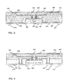
- FIG. 3 illustrates a cross section of an exemplary arrangement not forming part of the invention.
- the arrangement comprises a substrate 363, which is e.g. Kapton film.
- the ASIC processing/measurement circuit 380 is attached on the carrier 363.
- the unit is connected to a printed circuit board by soldering from its soldering balls 367 and 368.
- the ASIC circuit is coupled electrically to the soldering balls by wire bonding 361, 362 to metallizations 375, 376 on the substrate.
- the driver electrode 321 and the sensing electrodes 322 are connected to the ASIC circuit with wires made by metallizations and vias, 323 and 324.
- the electrodes are made closer to the surface of the unit by producing polymer bumps 365 and 366 to the microreplicated polymer layer 367.
- the thickness of the bumps is e.g. 100 - 200 ⁇ m.
- Figure 4 illustrates a cross section of another exemplary arrangement not forming part of the invention.
- the arrangement is similar with the previous embodiment of Figure 3 , but the contacts from the ASIC to the soldering balls are made with metal film connection vias 461, 462 to the printed metallizations 475, 476 of the substrate.
- This arrangement requires a thinned ASIC circuit so that the vias 461, 462 do not need to be very deep.
- Figure 5 illustrates a cross section of a third exemplary arrangement according to the invention.
- the arrangement is similar with the previous embodiments, but in this arrangement the ASIC is electrically coupled directly to a flexible substrate or "flex" 563.
- the electrodes 521, 522 and the ASIC 580 are on opposite sides of the substrate.
- the electrodes are connected to the ASIC with vias 523, 524, which extend to the surface of the ASIC through holes on the substrate.
- the unit is preferably connected to other electronics with a connector at the end of the flex 563.
- the flexible substrate is preferably Kapton film.
- Figure 6 illustrates a cross section of a fourth exemplary arrangement according to the invention.
- the arrangement is similar with the previous embodiment of Figure 5 , but in this arrangement the unit is soldered to other electronics. This is achieved by bending 669 and attaching the flex 663 under the unit, and further connecting soldering balls 679 to the flex 663.
- the layers 625 and 668 are produced by encapsulation.
- Figure 7A illustrates a cross section of a fifth exemplary arrangement according to the invention.
- the arrangement is similar with the previous embodiment of Figure 5 , but in this arrangement the metallizations 723, 724 between the ASIC 780 and the electrodes 721, 722 are located on the flex substrate 763 thus avoiding one layer of microreplicated polymer and reducing the depth of the vias.
- Figure 7B illustrates a top view of the arrangement shown in Figure 7A , without the top capsulation.
- Figure 7B shows the drive electrode 721, which is located on the polymer layer 765.
- the driver electrode is connected through the via 723 to the ASIC.
- the Figure also shows the array of sensing electrodes 722 with guard rings 729. The sensing electrodes and guard rings are wired by metallizations to array of the vias 724.
- Figure 8 illustrates a cross section of a sixth exemplary arrangement according to the invention.
- the arrangement is similar with the previous embodiment of Figure 7 , but in this arrangement there are guard electrodes 827, 828 under the sensing electrode metallizations.
- the guard electrodes and sensing electrodes are both connected to the ASIC with vias, 826, 824.
- Figure 9 illustrates top and cross section views of exemplary sensing electrodes 922 and guard electrodes 928 on a substrate 963.
- the guard electrodes 928 are located under the sensing electrodes 922 with an insulating layer 929 between the electrodes. In this embodiment the guard electrodes have larger surface.
- a buffer amplifier 985 keeps the guard electrodes in the same potential as the sensor electrodes and thus the sensor electrodes are less loaded by the adjacent materials, or interference.
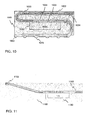
- Figure 10 illustrates a further modification of an arrangement where the connection to other electronics is made by bending a flexible printed wired board (FWB) or film substrate 1063 to under the unit, and attaching soldering balls 1078 to the flex.
- the other end of the flex is bent above the unit in order to use the other end of the flex as electrodes.
- the wiring to the electrodes 1022 and to the soldering balls 1078 is provided using two-sided metallization 1030, 1034 of the flex film and vias 1023, 1024.
- On the electrode end of the flex one metallized surface 1030 serves as sensing electrode and the second metallized surface 1034 of the flex serves as a guard electrode. This construction enables a two- or three-dimensional form of the electrode-finger interface.
- Figure 11 illustrates another embodiment where one end of a flexible printed, wired substrate is used for electrodes 1122, and other part of the flex 1163 for external connection.
- the connections between the metallized surfaces and the ASIC 1180 can be made similar to the embodiment of Figure 10 .
- This construction also enables a two- or three-dimensional form of the electrode-finger interface. This arrangement can be directly molded into a cover 1168 of e.g. mobile phone.
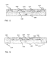
- Figure 12 illustrates a cross section of a further exemplary arrangement according to the invention.
- the ASIC circuit 1280 is large in respect of the needed electrode structure, and therefore it is possible to create a two- or three-dimensional form of the electrode structure directly on the ASIC.
- the sensing electrodes 1222 and the driver electrode 1221 are produced on polymer bumps 1266.
- the connections to the soldering balls 1277 and 1278 are also made using similar polymer bumps and metallizations.
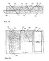
- Figure 13 illustrates a cross section of a still further exemplary arrangement according to the invention. This embodiment is similar to the arrangement of Figure 12 , but in this arrangement there is a substrate 1363 and bonding wires 1361, 1362 for creating connections from the ASIC 1280 to the metallized pads of the substrate 1363 and the soldering balls 1377, 1378.
- Figure 14 illustrates a cross section of a further exemplary arrangement according to the invention. This embodiment is similar to the arrangement of Figure 13 , but instead of bonding wires the connections 1461, 1462 between the ASIC 1480 and the substrate 1463 are made using metallization.
- Figure 15 illustrates a cross section of a further exemplary arrangement according to the invention.
- This embodiment is similar to the arrangement of Figure 12 , but this embodiment includes a polymer layer 1525 with preferably 100-150 ⁇ m deep grooves 1565.
- the soldering balls 1577, 1578 are first attached to holes in the polymer, and metallizations 1521, 1522 that form the electrodes are made on the grooves in the opposite side of the polymer.
- the polymer substrate 1525 is then attached on the ASIC, 1580.
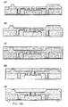
- FIGS 16A and 16B illustrate an exemplary process for manufacturing a unit of Figure 4 according to the invention.
- the Figures show a cross section of the unit to be manufactured after the concerned manufacturing phase has been executed.
- First in phase 160 an ASIC circuit is glued on a flexible substrate that includes wiring.
- the ASIC is preferably a thinned type component with height of only 50 - 100 ⁇ m.
- the flex sheet substrate may be large for attachment of several components.
- step 161 a polymer layer is cast on top of the attached ASIC.
- vias are opened through the polymer layer until the wiring of the flex substrate and to the ASIC pads.
- the metallization is then electroplated and patterned in step 163.
- the polymer layer is injection molded using micro replicated mold, step 164.
- vias are opened through the polymer layer to the ASIC pads in step 165. This may also be made by cavity molding during the previous step.
- step 166 the electroplated metallization is patterned to form the electrode structure.
- a protective polymer layer is cast on top of the device in step 167.
- the solder areas of the substrate are then opened, step 168, and finally the solder bumps are processed and diced in step 169.
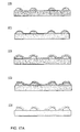
- FIGS 17A and 17B illustrate another exemplary process, which is for manufacturing a unit of Figure 12 according to the invention.
- phase 170 two or three dimensionally formed structures are fabricated on top of the ASIC surface with roughly 100-200 ⁇ m of height.
- the thin film metallization is deposited on top of the ASIC and the 3D polymer structures in phase 171.
- the metallization can be made using e.g. Cr-Au.
- step 172 a photoresist is electroplated on top of the metallization.
- the photoresist is then patterned, step 173, and the metal layers are etched in step 174.
- step 17B the photoresist is removed in step 175.
- a protective polymer layer is cast in step 176, and contact areas are opened for the flip-chip process, step 177.
- the soldering balls are then attached with flip-chip bump process in step 178, and finally the produced unit is attached to a cover, step 179.
Landscapes
- Engineering & Computer Science (AREA)
- Physics & Mathematics (AREA)
- General Physics & Mathematics (AREA)
- Human Computer Interaction (AREA)
- Multimedia (AREA)
- Theoretical Computer Science (AREA)
- Microelectronics & Electronic Packaging (AREA)
- Image Input (AREA)
- Measurement Of Length, Angles, Or The Like Using Electric Or Magnetic Means (AREA)
- Measurement Of The Respiration, Hearing Ability, Form, And Blood Characteristics Of Living Organisms (AREA)
Claims (38)
- Fingerabdruck-Sensoranordnung, umfassend eine Treiberelektrode (521, 621, 721, 821) und eine Sensorelektrode (522, 622, 722, 822) für eine kapazitive Messung, und eine integrierte Signalverarbeitungsschaltung (580, 680, 780, 880, 1080) für eine Messung von Signalen von der Treiberelektrode und der Sensorelektrode, und eine Verbindungsverdrahtung (523, 524, 623, 624, 723, 724, 823, 824) zwischen der Treiberelektrode und der Sensorelektrode und der integrierten Signalverarbeitungsschaltung,
dadurch gekennzeichnet, dass
die Anordnung ein Substrat (563, 663, 763, 863) aus einem flexiblen Material umfasst, wobei das Substrat so eingerichtet ist, dass ein Ende des Substrats als die Treiberelektrode oder die Sensorelektrode verwendet wird, oder wobei das Substrat aus flexiblem Material mit der Treiberelektrode und der Sensorelektrode gekoppelt ist; und
die Treiberelektrode, die Sensorelektrode, die integrierte Signalverarbeitungsschaltung und die Verbindungsverdrahtung in einem integrierten Modul eingebettet sind, und wobei die Verbindungsverdrahtung eine Metallisierung zwischen Polymerlagen (525, 565) ist und die Treiberelektrode oder die Sensorelektrode eine Metallisierung zwischen den Polymerlagen ist. - Anordnung gemäß Anspruch 1, wobei die Elektroden und die integrierte Schaltung mit dem Substrat (1063, 1163) gekoppelt sind, wobei das Substrat die Verdrahtung (1030, 1122) zwischen den Elektroden und der integrierten Schaltung umfasst.
- Anordnung gemäß Anspruch 1, wobei das Substrat die Treiberelektrode oder die Sensorelektrode umfasst.
- Anordnung gemäß Anspruch 1, wobei das Substrat eine Verdrahtung (1063, 1163) für eine externe Verbindung mit der integrierten Schaltung umfasst.
- Anordnung gemäß Anspruch 4, die eine Metallisierung zwischen der integrierten Schaltung und der Verdrahtung des Substrats umfasst.
- Anordnung gemäß Anspruch 1, wobei die Treiberelektrode und die Sensorelektrode Metallisierungen zwischen den Polymerlagen (525, 565, 566) sind.
- Anordnung gemäß Anspruch 1, die Schutzringe (827, 828) in einer Nähe der Treiberelektrode oder der Sensorelektrode umfasst.
- Anordnung gemäß Anspruch 7, die eine isolierende Polymerlage (929) zwischen einer Schutzring-Metallisierung (928) und der Sensorelektrode umfasst.
- Anordnung gemäß Anspruch 1, wobei das integrierte Modul mit spritzgegossenem Polymer eingekapselt ist.
- Anordnung gemäß Anspruch 1, wobei eine Oberfläche des Sensors eine gekrümmte Form in mindestens zwei Dimensionen aufweist.
- Anordnung gemäß Anspruch 10, wobei die Form einer Form eines Fingers angenähert ist.
- Anordnung gemäß Anspruch 1, umfassend eine Erhebung (565, 566), um die Elektroden zu erhöhen.
- Anordnung gemäß Anspruch 12, wobei die Erhebung eine Lage aus Polymer ist.
- Anordnung gemäß Anspruch 1, wobei der Sensor die Treiberelektrode, eine Reihe von Sensorelektroden und eine Messschaltung umfasst, die eingerichtet ist, aufeinander folgende Signale zu messen während sich ein Finger in einer in Bezug auf die Reihe der Sensorelektroden senkrechten Richtung bewegt, um eine zweidimensionale Matrix von kapazitiven Messergebnissen des Fingers bereitzustellen.
- Anordnung gemäß Anspruch 1, weiter umfassend eine Infrarot-Lichtquelle, einen Infrarotlicht-Detektor und zweite Messmittel, zum Messen der Absorption von Infrarotlicht eines Fingers.
- Anordnung gemäß Anspruch 1, weiter umfassend einen Temperatursensor zum Messen einer Temperatur eines Fingers.
- Anordnung gemäß Anspruch 1, weiter umfassend einen Feuchtigkeitssensor zum Messen der Feuchtigkeit des Fingers.
- Mobiles Endgerät, dadurch gekennzeichnet, dass das mobile Endgerät die Fingerabdruck-Sensoranordnung eines der vorstehenden Ansprüche umfasst.
- Verfahren zum Herstellen einer Fingerabdruck-Sensoranordnung, umfassend:Bereitstellen einer integrierten Signalverarbeitungsschaltung (160, 170),wobei das Verfahren weiter umfasstBereitstellen einer Treiberelektrode (166, 171-175); undBereitstellen einer Sensorelektrode (166, 171-175) für kapazitive Messung, sodass ein Substrat aus einem flexiblen Material so eingerichtet ist, dass ein Ende des Substrats als die Treiberelektrode oder die Sensorelektrode verwendet wird, oder so eingerichtet ist, dass das Substrat aus dem flexiblen Material mit der Treiberelektrode und der Sensorelektrode gekoppelt ist; undEinkapseln der integrierten Signalverarbeitungsschaltung, der Treiberelektrode und der Sensorelektrode in ein integriertes Modul (160-167, 170-176), wobei eine Verbindungsverdrahtung zwischen der Treiberelektrode und der Sensorelektrode und der integrierten Signalverarbeitungsschaltung eine Metallisierung zwischen Polymerlagen ist und die Treiberelektrode oder die Sensorelektrode eine Metallisierung zwischen den Polymerlagen ist.
- Verfahren gemäß Anspruch 19, wobei der Schritt des Einkapselns ein Einkapseln in Polymer (161, 164, 167, 176) umfasst.
- Verfahren gemäß Anspruch 19, wobei der Schritt des Bereitstellens der Treiberelektrode Metallisieren (166, 171) umfasst.
- Verfahren gemäß Anspruch 19, wobei der Schritt des Bereitstellens der Sensorelektrode Metallisieren umfasst.
- Verfahren gemäß Anspruch 19, umfassend Bereitstellen eines Schutzrings in einer Nähe der Treiberelektrode oder der Sensorelektrode.
- Verfahren gemäß Anspruch 23, wobei der Schritt des Bereitstellens des Schutzrings Metallisieren umfasst.
- Verfahren gemäß Anspruch 23, umfassend einen Schritt des Bereitstellens einer isolierenden Polymerlage zwischen dem Schutzring und der Sensorelektrode.
- Verfahren gemäß Anspruch 19, umfassend einen Schritt des Bereitstellens eines Substrats und Verbinden der integrierten Signalverarbeitungsschaltung auf dem Substrat (160) vor dem Einkapseln.
- Verfahren gemäß Anspruch 26, umfassend einen Schritt des Bereitstellens einer Öffnung in dem Substrat (168) zum Bereitstellen einer elektrischen Verbindung durch das Substrat.
- Verfahren gemäß Anspruch 19, umfassend einen Schritt des Bereitstellens einer erhöhenden Erhebung zwischen dem Substrat und den Elektroden.
- Verfahren gemäß Anspruch 28, wobei die Erhebung aus einer Lage aus Polymer gebildet ist.
- Verfahren gemäß Anspruch 26, wobei das Substrat eine flexible Schicht ist und eine Verdrahtung einschließt.
- Verfahren gemäß Anspruch 30, wobei ein Ende des flexiblen Substrats verwendet wird, um externe Schaltungen elektrisch mit dem Fingerabdrucksensor zu verbinden.
- Verfahren gemäß Anspruch 30, wobei die Verdrahtung des flexiblen Substrats zum Bereitstellen der Sensorelektrode oder der Treiberelektrode verwendet wird.
- Verfahren gemäß Anspruch 19, wobei die Sensorelektrode oder die Treiberelektrode auf einer Oberfläche der integrierten Signalverarbeitungsschaltung mit Metallisieren bereitgestellt wird.
- Verfahren gemäß Anspruch 26, wobei eine elektrische Verbindung zwischen der integrierten Signalverarbeitungsschaltung und der Verdrahtung des Substrats durch Drahtbonden bereitgestellt wird.
- Verfahren gemäß Anspruch 26, wobei eine elektrische Verbindung zwischen der integrierten Signalverarbeitungsschaltung und der Verdrahtung des Substrats (163) durch Metallisieren bereitgestellt wird.
- Verfahren gemäß Anspruch 19, wobei eine Polymerlage durch Spritzgießen unter Verwendung einer Mikro-Replikationsform( 164) bereitgestellt wird.
- Verfahren gemäß einem der Ansprüche 19 - 36, umfassend die Schritte des Bereitstellens von Polymerlagen (161, 164, 168, 170, 176) und mindestens einer Metallisierungslage (163, 166, 171), eine auf der anderen.
- Verfahren gemäß Anspruch 19, wobei der Fingerabdrucksensor in eine Ausrüstungsabdeckung eingebettet ist.
Applications Claiming Priority (3)
| Application Number | Priority Date | Filing Date | Title |
|---|---|---|---|
| FI20030102A FI20030102A0 (fi) | 2003-01-22 | 2003-01-22 | Henkilön varmennusjärjestely |
| FI20030102 | 2003-01-22 | ||
| PCT/FI2004/000032 WO2004066693A1 (en) | 2003-01-22 | 2004-01-22 | Arrangement for authentication of a person |
Publications (2)
| Publication Number | Publication Date |
|---|---|
| EP1588595A1 EP1588595A1 (de) | 2005-10-26 |
| EP1588595B1 true EP1588595B1 (de) | 2011-09-14 |
Family
ID=8565414
Family Applications (1)
| Application Number | Title | Priority Date | Filing Date |
|---|---|---|---|
| EP04704246A Expired - Lifetime EP1588595B1 (de) | 2003-01-22 | 2004-01-22 | Anordnung zum Authentifizieren einer Person |
Country Status (8)
| Country | Link |
|---|---|
| US (1) | US7606400B2 (de) |
| EP (1) | EP1588595B1 (de) |
| JP (1) | JP2006517023A (de) |
| KR (1) | KR100759117B1 (de) |
| CN (1) | CN1802882B (de) |
| CA (1) | CA2514067C (de) |
| FI (1) | FI20030102A0 (de) |
| WO (1) | WO2004066693A1 (de) |
Families Citing this family (93)
| Publication number | Priority date | Publication date | Assignee | Title |
|---|---|---|---|---|
| DE60114241T2 (de) | 2000-12-05 | 2006-07-13 | Validity Sensors Inc., Phoenix | System und methode zur kapazitiven aufnahme von fingerabdrücken durch überstreichen |
| FI20030102A0 (fi) * | 2003-01-22 | 2003-01-22 | Nokia Corp | Henkilön varmennusjärjestely |
| US8229184B2 (en) | 2004-04-16 | 2012-07-24 | Validity Sensors, Inc. | Method and algorithm for accurate finger motion tracking |
| US8358815B2 (en) | 2004-04-16 | 2013-01-22 | Validity Sensors, Inc. | Method and apparatus for two-dimensional finger motion tracking and control |
| US8165355B2 (en) | 2006-09-11 | 2012-04-24 | Validity Sensors, Inc. | Method and apparatus for fingerprint motion tracking using an in-line array for use in navigation applications |
| US8175345B2 (en) | 2004-04-16 | 2012-05-08 | Validity Sensors, Inc. | Unitized ergonomic two-dimensional fingerprint motion tracking device and method |
| US8447077B2 (en) | 2006-09-11 | 2013-05-21 | Validity Sensors, Inc. | Method and apparatus for fingerprint motion tracking using an in-line array |
| US8131026B2 (en) | 2004-04-16 | 2012-03-06 | Validity Sensors, Inc. | Method and apparatus for fingerprint image reconstruction |
| EP1754180A1 (de) | 2004-04-16 | 2007-02-21 | Validity Sensors Inc. | Fingerpositions-erfassungsverfahren und -vorrichtungen |
| US8077935B2 (en) | 2004-04-23 | 2011-12-13 | Validity Sensors, Inc. | Methods and apparatus for acquiring a swiped fingerprint image |
| WO2006041780A1 (en) * | 2004-10-04 | 2006-04-20 | Validity Sensors, Inc. | Fingerprint sensing assemblies comprising a substrate |
| US7460697B2 (en) | 2005-07-19 | 2008-12-02 | Validity Sensors, Inc. | Electronic fingerprint sensor with differential noise cancellation |
| US8358816B2 (en) * | 2005-10-18 | 2013-01-22 | Authentec, Inc. | Thinned finger sensor and associated methods |
| US7424136B2 (en) | 2005-10-18 | 2008-09-09 | Authentec, Inc. | Finger sensing with enhanced mounting and associated methods |
| DE102005051530A1 (de) * | 2005-10-26 | 2007-05-03 | Joachim Aurich | Ausleseverfahren für Sensorfelder, insbesondere für Fingerabdruck-Sensoren |
| JP4725385B2 (ja) * | 2006-03-24 | 2011-07-13 | ソニー株式会社 | 携帯型電話機及び電子機器 |
| GB2436636A (en) * | 2006-03-28 | 2007-10-03 | Avantone Oy | Machine readable conductive array and devices for reading the same |
| US7859116B1 (en) | 2006-12-26 | 2010-12-28 | Amkor Technology, Inc. | Exposed metal bezel for use in sensor devices and method therefor |
| US8107212B2 (en) | 2007-04-30 | 2012-01-31 | Validity Sensors, Inc. | Apparatus and method for protecting fingerprint sensing circuitry from electrostatic discharge |
| US8290150B2 (en) | 2007-05-11 | 2012-10-16 | Validity Sensors, Inc. | Method and system for electronically securing an electronic device using physically unclonable functions |
| US20110002461A1 (en) * | 2007-05-11 | 2011-01-06 | Validity Sensors, Inc. | Method and System for Electronically Securing an Electronic Biometric Device Using Physically Unclonable Functions |
| KR100914615B1 (ko) * | 2007-09-10 | 2009-09-02 | 주식회사 유니온커뮤니티 | 생체지문을 구별하여 인식하는 지문인식장치 및 방법 |
| US8204281B2 (en) * | 2007-12-14 | 2012-06-19 | Validity Sensors, Inc. | System and method to remove artifacts from fingerprint sensor scans |
| US8276816B2 (en) | 2007-12-14 | 2012-10-02 | Validity Sensors, Inc. | Smart card system with ergonomic fingerprint sensor and method of using |
| US8073204B2 (en) * | 2007-12-31 | 2011-12-06 | Authentec, Inc. | Hybrid multi-sensor biometric identification device |
| US8116540B2 (en) | 2008-04-04 | 2012-02-14 | Validity Sensors, Inc. | Apparatus and method for reducing noise in fingerprint sensing circuits |
| US8005276B2 (en) | 2008-04-04 | 2011-08-23 | Validity Sensors, Inc. | Apparatus and method for reducing parasitic capacitive coupling and noise in fingerprint sensing circuits |
| GB2474999B (en) * | 2008-07-22 | 2013-02-20 | Validity Sensors Inc | System and method for securing a device component |
| JP2010103240A (ja) * | 2008-10-22 | 2010-05-06 | Fujitsu Ltd | 接触センサユニット、電子装置及び接触センサユニットの製造方法 |
| US8391568B2 (en) | 2008-11-10 | 2013-03-05 | Validity Sensors, Inc. | System and method for improved scanning of fingerprint edges |
| US20100176892A1 (en) * | 2009-01-15 | 2010-07-15 | Validity Sensors, Inc. | Ultra Low Power Oscillator |
| US8278946B2 (en) * | 2009-01-15 | 2012-10-02 | Validity Sensors, Inc. | Apparatus and method for detecting finger activity on a fingerprint sensor |
| US20100180136A1 (en) * | 2009-01-15 | 2010-07-15 | Validity Sensors, Inc. | Ultra Low Power Wake-On-Event Mode For Biometric Systems |
| US8600122B2 (en) | 2009-01-15 | 2013-12-03 | Validity Sensors, Inc. | Apparatus and method for culling substantially redundant data in fingerprint sensing circuits |
| US8374407B2 (en) | 2009-01-28 | 2013-02-12 | Validity Sensors, Inc. | Live finger detection |
| US20100208953A1 (en) * | 2009-02-17 | 2010-08-19 | Validity Sensors, Inc. | Illuminated Fingerprint Sensor and Method |
| TW201044284A (en) * | 2009-06-09 | 2010-12-16 | Egis Technology Inc | Image sensing device adapted to flat surface design |
| US9274553B2 (en) | 2009-10-30 | 2016-03-01 | Synaptics Incorporated | Fingerprint sensor and integratable electronic display |
| US9400911B2 (en) | 2009-10-30 | 2016-07-26 | Synaptics Incorporated | Fingerprint sensor and integratable electronic display |
| US9336428B2 (en) | 2009-10-30 | 2016-05-10 | Synaptics Incorporated | Integrated fingerprint sensor and display |
| NO20093601A1 (no) | 2009-12-29 | 2011-06-30 | Idex Asa | Overflatesensor |
| US8421890B2 (en) | 2010-01-15 | 2013-04-16 | Picofield Technologies, Inc. | Electronic imager using an impedance sensor grid array and method of making |
| US8791792B2 (en) * | 2010-01-15 | 2014-07-29 | Idex Asa | Electronic imager using an impedance sensor grid array mounted on or about a switch and method of making |
| US8866347B2 (en) | 2010-01-15 | 2014-10-21 | Idex Asa | Biometric image sensing |
| US9666635B2 (en) | 2010-02-19 | 2017-05-30 | Synaptics Incorporated | Fingerprint sensing circuit |
| US8716613B2 (en) | 2010-03-02 | 2014-05-06 | Synaptics Incoporated | Apparatus and method for electrostatic discharge protection |
| US9001040B2 (en) | 2010-06-02 | 2015-04-07 | Synaptics Incorporated | Integrated fingerprint sensor and navigation device |
| US8736001B2 (en) | 2010-06-18 | 2014-05-27 | Authentec, Inc. | Finger sensor including encapsulating layer over sensing area and related methods |
| US8717775B1 (en) | 2010-08-02 | 2014-05-06 | Amkor Technology, Inc. | Fingerprint sensor package and method |
| US8331096B2 (en) | 2010-08-20 | 2012-12-11 | Validity Sensors, Inc. | Fingerprint acquisition expansion card apparatus |
| CN102148222B (zh) * | 2010-12-18 | 2012-07-18 | 日月光半导体制造股份有限公司 | 具邻近通信信号输入端的半导体结构及半导体封装结构 |
| US8594393B2 (en) | 2011-01-26 | 2013-11-26 | Validity Sensors | System for and method of image reconstruction with dual line scanner using line counts |
| US8538097B2 (en) | 2011-01-26 | 2013-09-17 | Validity Sensors, Inc. | User input utilizing dual line scanner apparatus and method |
| US9406580B2 (en) * | 2011-03-16 | 2016-08-02 | Synaptics Incorporated | Packaging for fingerprint sensors and methods of manufacture |
| US10043052B2 (en) | 2011-10-27 | 2018-08-07 | Synaptics Incorporated | Electronic device packages and methods |
| US9195877B2 (en) | 2011-12-23 | 2015-11-24 | Synaptics Incorporated | Methods and devices for capacitive image sensing |
| US9785299B2 (en) | 2012-01-03 | 2017-10-10 | Synaptics Incorporated | Structures and manufacturing methods for glass covered electronic devices |
| US9137438B2 (en) | 2012-03-27 | 2015-09-15 | Synaptics Incorporated | Biometric object sensor and method |
| US9251329B2 (en) | 2012-03-27 | 2016-02-02 | Synaptics Incorporated | Button depress wakeup and wakeup strategy |
| US9268991B2 (en) | 2012-03-27 | 2016-02-23 | Synaptics Incorporated | Method of and system for enrolling and matching biometric data |
| US9600709B2 (en) | 2012-03-28 | 2017-03-21 | Synaptics Incorporated | Methods and systems for enrolling biometric data |
| US9152838B2 (en) | 2012-03-29 | 2015-10-06 | Synaptics Incorporated | Fingerprint sensor packagings and methods |
| EP2836960B1 (de) | 2012-04-10 | 2018-09-26 | Idex Asa | Biometrische erfassung |
| US9740343B2 (en) | 2012-04-13 | 2017-08-22 | Apple Inc. | Capacitive sensing array modulation |
| US9581628B2 (en) * | 2012-05-04 | 2017-02-28 | Apple Inc. | Electronic device including device ground coupled finger coupling electrode and array shielding electrode and related methods |
| US9030440B2 (en) | 2012-05-18 | 2015-05-12 | Apple Inc. | Capacitive sensor packaging |
| US8616451B1 (en) | 2012-06-21 | 2013-12-31 | Authentec, Inc. | Finger sensing device including finger sensing integrated circuit die within a recess in a mounting substrate and related methods |
| US8816500B2 (en) * | 2012-12-14 | 2014-08-26 | Infineon Technologies Ag | Semiconductor device having peripheral polymer structures |
| US9665762B2 (en) | 2013-01-11 | 2017-05-30 | Synaptics Incorporated | Tiered wakeup strategy |
| US9883822B2 (en) | 2013-06-05 | 2018-02-06 | Apple Inc. | Biometric sensor chip having distributed sensor and control circuitry |
| NL2012891B1 (en) | 2013-06-05 | 2016-06-21 | Apple Inc | Biometric sensor chip having distributed sensor and control circuitry. |
| KR101301063B1 (ko) * | 2013-07-05 | 2013-08-28 | (주)드림텍 | 고유전율 재료를 이용한 지문인식 홈키 제조방법 및 지문인식 홈키 구조 |
| NO336318B1 (no) * | 2013-07-12 | 2015-08-03 | Idex Asa | Overflatesensor |
| US9984270B2 (en) | 2013-08-05 | 2018-05-29 | Apple Inc. | Fingerprint sensor in an electronic device |
| KR20150018350A (ko) | 2013-08-08 | 2015-02-23 | 삼성전자주식회사 | 지문인식장치와 그 제조방법 및 전자기기 |
| US10296773B2 (en) | 2013-09-09 | 2019-05-21 | Apple Inc. | Capacitive sensing array having electrical isolation |
| US9460332B1 (en) | 2013-09-09 | 2016-10-04 | Apple Inc. | Capacitive fingerprint sensor including an electrostatic lens |
| US9697409B2 (en) | 2013-09-10 | 2017-07-04 | Apple Inc. | Biometric sensor stack structure |
| US20150091588A1 (en) * | 2013-10-01 | 2015-04-02 | Synaptics Incorporated | Compact and durable button with biometric sensor having improved sensor signal production and method for making same |
| JP2017511162A (ja) * | 2014-01-29 | 2017-04-20 | サムスン エレクトロニクス カンパニー リミテッド | 指紋認識装置とその製造方法および電子機器 |
| TWI493187B (zh) * | 2014-02-17 | 2015-07-21 | 茂丞科技股份有限公司 | 藉由信號外延結構形成之具有平坦接觸面之生物感測器及其製造方法 |
| US9582127B2 (en) | 2014-04-04 | 2017-02-28 | Synaptics Incorporated | Large feature biometrics using capacitive touchscreens |
| CN104051367A (zh) * | 2014-07-01 | 2014-09-17 | 苏州晶方半导体科技股份有限公司 | 指纹识别芯片封装结构和封装方法 |
| US9558390B2 (en) * | 2014-07-25 | 2017-01-31 | Qualcomm Incorporated | High-resolution electric field sensor in cover glass |
| US10043847B2 (en) * | 2014-08-26 | 2018-08-07 | Gingy Technology Inc. | Image capturing module and electrical apparatus |
| USD776664S1 (en) * | 2015-05-20 | 2017-01-17 | Chaya Coleena Hendrick | Smart card |
| CN105138988B (zh) | 2015-08-26 | 2020-02-21 | 京东方科技集团股份有限公司 | 互容式指纹识别器件及制备方法、显示面板及显示设备 |
| KR20170082358A (ko) * | 2016-01-06 | 2017-07-14 | 하나 마이크론(주) | 스마트 기기의 트랙패드 반도체 패키지 및 그 제조 방법 |
| WO2017171887A1 (en) * | 2016-04-02 | 2017-10-05 | Intel Corporation | Flexible circuit interconnect structure and method of making same |
| CN106203303B (zh) * | 2016-06-30 | 2018-02-02 | 北京小米移动软件有限公司 | 指纹识别装置及方法 |
| CN106250882A (zh) * | 2016-08-26 | 2016-12-21 | 广东欧珀移动通信有限公司 | 指纹识别感测装置、电子设备和移动终端 |
| CN106372586B (zh) * | 2016-08-26 | 2018-03-06 | 广东欧珀移动通信有限公司 | 指纹识别感测装置、电子设备和移动终端 |
| CN110197539B (zh) * | 2018-02-27 | 2022-07-12 | 江西欧迈斯微电子有限公司 | 指纹识别模组和指纹识别门锁 |
Citations (2)
| Publication number | Priority date | Publication date | Assignee | Title |
|---|---|---|---|---|
| EP0786745A2 (de) * | 1996-01-26 | 1997-07-30 | Harris Corporation | Verbessertes Gehäuse für Sicherheitsfingerabdrucksensor und zugehörige Verfahren |
| WO2004066693A1 (en) * | 2003-01-22 | 2004-08-05 | Nokia Corporation | Arrangement for authentication of a person |
Family Cites Families (19)
| Publication number | Priority date | Publication date | Assignee | Title |
|---|---|---|---|---|
| US4577345A (en) * | 1984-04-05 | 1986-03-18 | Igor Abramov | Fingerprint sensor |
| JPH06104641A (ja) | 1992-09-22 | 1994-04-15 | Nikko Electron Kk | 表面実装型発振器 |
| US6067368A (en) | 1996-01-26 | 2000-05-23 | Authentec, Inc. | Fingerprint sensor having filtering and power conserving features and related methods |
| FR2749955B1 (fr) * | 1996-06-14 | 1998-09-11 | Thomson Csf | Systeme de lecture d'empreintes digitales |
| US6088585A (en) | 1997-05-16 | 2000-07-11 | Authentec, Inc. | Portable telecommunication device including a fingerprint sensor and related methods |
| US5887343A (en) | 1997-05-16 | 1999-03-30 | Harris Corporation | Direct chip attachment method |
| JP2959532B2 (ja) | 1997-06-30 | 1999-10-06 | 日本電気株式会社 | 静電容量検出方式の指紋画像入力装置 |
| GB9725571D0 (en) * | 1997-12-04 | 1998-02-04 | Philips Electronics Nv | Electronic apparatus comprising fingerprint sensing devices |
| ATE222010T1 (de) | 1998-05-19 | 2002-08-15 | Infineon Technologies Ag | Sensoreinrichtung zur erfassung von biometrischen merkmalen, insbesondere fingerminutien |
| US6161403A (en) * | 1999-06-28 | 2000-12-19 | Surratt; James E. | Bicycle steering lock |
| WO2001006448A1 (en) | 1999-07-14 | 2001-01-25 | Veridicom, Inc. | Ultra-rugged i.c. sensor and method of making the same |
| US6423995B1 (en) | 1999-07-26 | 2002-07-23 | Stmicroelectronics, Inc. | Scratch protection for direct contact sensors |
| JP3966397B2 (ja) | 1999-12-27 | 2007-08-29 | シャープ株式会社 | 指紋検出装置 |
| US6643389B1 (en) * | 2000-03-28 | 2003-11-04 | Stmicroelectronics, Inc. | Narrow array capacitive fingerprint imager |
| NO315016B1 (no) | 2000-06-09 | 2003-06-23 | Idex Asa | Miniatyrisert sensor |
| NO315017B1 (no) * | 2000-06-09 | 2003-06-23 | Idex Asa | Sensorbrikke, s¶rlig for måling av strukturer i en fingeroverflate |
| DE60114241T2 (de) * | 2000-12-05 | 2006-07-13 | Validity Sensors Inc., Phoenix | System und methode zur kapazitiven aufnahme von fingerabdrücken durch überstreichen |
| JP2003016433A (ja) | 2001-07-03 | 2003-01-17 | Nec Corp | 指紋照合における生体識別方法,方式,およびプログラム |
| US7006078B2 (en) * | 2002-05-07 | 2006-02-28 | Mcquint, Inc. | Apparatus and method for sensing the degree and touch strength of a human body on a sensor |
-
2003
- 2003-01-22 FI FI20030102A patent/FI20030102A0/fi unknown
-
2004
- 2004-01-22 KR KR1020057013518A patent/KR100759117B1/ko not_active Expired - Fee Related
- 2004-01-22 US US10/763,821 patent/US7606400B2/en active Active
- 2004-01-22 JP JP2005518431A patent/JP2006517023A/ja active Pending
- 2004-01-22 CA CA2514067A patent/CA2514067C/en not_active Expired - Fee Related
- 2004-01-22 WO PCT/FI2004/000032 patent/WO2004066693A1/en not_active Ceased
- 2004-01-22 EP EP04704246A patent/EP1588595B1/de not_active Expired - Lifetime
- 2004-01-22 CN CN2004800026612A patent/CN1802882B/zh not_active Expired - Lifetime
Patent Citations (2)
| Publication number | Priority date | Publication date | Assignee | Title |
|---|---|---|---|---|
| EP0786745A2 (de) * | 1996-01-26 | 1997-07-30 | Harris Corporation | Verbessertes Gehäuse für Sicherheitsfingerabdrucksensor und zugehörige Verfahren |
| WO2004066693A1 (en) * | 2003-01-22 | 2004-08-05 | Nokia Corporation | Arrangement for authentication of a person |
Also Published As
| Publication number | Publication date |
|---|---|
| US7606400B2 (en) | 2009-10-20 |
| WO2004066693A1 (en) | 2004-08-05 |
| JP2006517023A (ja) | 2006-07-13 |
| WO2004066693A8 (en) | 2005-11-03 |
| CN1802882B (zh) | 2010-11-10 |
| US20050031174A1 (en) | 2005-02-10 |
| KR100759117B1 (ko) | 2007-09-19 |
| CA2514067C (en) | 2010-09-07 |
| CA2514067A1 (en) | 2004-08-05 |
| FI20030102A0 (fi) | 2003-01-22 |
| EP1588595A1 (de) | 2005-10-26 |
| KR20050107575A (ko) | 2005-11-14 |
| CN1802882A (zh) | 2006-07-12 |
Similar Documents
| Publication | Publication Date | Title |
|---|---|---|
| EP1588595B1 (de) | Anordnung zum Authentifizieren einer Person | |
| JP4708671B2 (ja) | 特に指紋センサのためのセンサチップ | |
| JP5491356B2 (ja) | センサ体及び該センサ体を備えた移動端末装置 | |
| EP3336759B1 (de) | Fingerabdruckerfassungsmodul und verfahren zur herstellung des fingerabdruckerfassungsmoduls | |
| US6672174B2 (en) | Fingerprint image capture device with a passive sensor array | |
| US8867799B2 (en) | Fingerprint sensing assemblies and methods of making | |
| KR101449226B1 (ko) | 용량성 렌즈를 포함하는 핑거 센서 및 연관된 방법 | |
| CN108021867B (zh) | 屏幕下方传感器组件 | |
| WO2008085771A2 (en) | Improved sensitivity capacitive sensor | |
| US11288476B2 (en) | Fingerprint sensor package | |
| JP2003086724A (ja) | 半導体装置および指紋検知装置 | |
| KR102204765B1 (ko) | 지문 센서와 버튼 조합들 및 그 제조 방법들 |
Legal Events
| Date | Code | Title | Description |
|---|---|---|---|
| PUAI | Public reference made under article 153(3) epc to a published international application that has entered the european phase |
Free format text: ORIGINAL CODE: 0009012 |
|
| 17P | Request for examination filed |
Effective date: 20050705 |
|
| AK | Designated contracting states |
Kind code of ref document: A1 Designated state(s): AT BE BG CH CY CZ DE DK EE ES FI FR GB GR HU IE IT LI LU MC NL PT RO SE SI SK TR |
|
| AX | Request for extension of the european patent |
Extension state: AL LT LV MK |
|
| RAP1 | Party data changed (applicant data changed or rights of an application transferred) |
Owner name: NOKIA CORPORATION |
|
| DAX | Request for extension of the european patent (deleted) | ||
| RBV | Designated contracting states (corrected) |
Designated state(s): DE ES FR GB IT |
|
| RIN1 | Information on inventor provided before grant (corrected) |
Inventor name: RYHAENEN, TAPANI Inventor name: HJELT, KARI |
|
| 17Q | First examination report despatched |
Effective date: 20091103 |
|
| GRAP | Despatch of communication of intention to grant a patent |
Free format text: ORIGINAL CODE: EPIDOSNIGR1 |
|
| RTI1 | Title (correction) |
Free format text: ARRANGEMENT FOR AUTHENTICATION OF A PERSON |
|
| GRAS | Grant fee paid |
Free format text: ORIGINAL CODE: EPIDOSNIGR3 |
|
| GRAA | (expected) grant |
Free format text: ORIGINAL CODE: 0009210 |
|
| AK | Designated contracting states |
Kind code of ref document: B1 Designated state(s): DE ES FR GB IT |
|
| REG | Reference to a national code |
Ref country code: GB Ref legal event code: FG4D |
|
| REG | Reference to a national code |
Ref country code: DE Ref legal event code: R081 Ref document number: 602004034313 Country of ref document: DE Owner name: NOKIA TECHNOLOGIES OY, FI Free format text: FORMER OWNER: NOKIA CORP., 02610 ESPOO, FI |
|
| REG | Reference to a national code |
Ref country code: DE Ref legal event code: R096 Ref document number: 602004034313 Country of ref document: DE Effective date: 20111117 |
|
| PG25 | Lapsed in a contracting state [announced via postgrant information from national office to epo] |
Ref country code: IT Free format text: LAPSE BECAUSE OF FAILURE TO SUBMIT A TRANSLATION OF THE DESCRIPTION OR TO PAY THE FEE WITHIN THE PRESCRIBED TIME-LIMIT Effective date: 20110914 |
|
| PLBE | No opposition filed within time limit |
Free format text: ORIGINAL CODE: 0009261 |
|
| STAA | Information on the status of an ep patent application or granted ep patent |
Free format text: STATUS: NO OPPOSITION FILED WITHIN TIME LIMIT |
|
| 26N | No opposition filed |
Effective date: 20120615 |
|
| GBPC | Gb: european patent ceased through non-payment of renewal fee |
Effective date: 20120122 |
|
| REG | Reference to a national code |
Ref country code: DE Ref legal event code: R097 Ref document number: 602004034313 Country of ref document: DE Effective date: 20120615 |
|
| REG | Reference to a national code |
Ref country code: FR Ref legal event code: ST Effective date: 20120928 |
|
| PG25 | Lapsed in a contracting state [announced via postgrant information from national office to epo] |
Ref country code: GB Free format text: LAPSE BECAUSE OF NON-PAYMENT OF DUE FEES Effective date: 20120122 |
|
| PG25 | Lapsed in a contracting state [announced via postgrant information from national office to epo] |
Ref country code: FR Free format text: LAPSE BECAUSE OF NON-PAYMENT OF DUE FEES Effective date: 20120131 |
|
| PG25 | Lapsed in a contracting state [announced via postgrant information from national office to epo] |
Ref country code: ES Free format text: LAPSE BECAUSE OF FAILURE TO SUBMIT A TRANSLATION OF THE DESCRIPTION OR TO PAY THE FEE WITHIN THE PRESCRIBED TIME-LIMIT Effective date: 20111225 |
|
| REG | Reference to a national code |
Ref country code: DE Ref legal event code: R081 Ref document number: 602004034313 Country of ref document: DE Owner name: NOKIA TECHNOLOGIES OY, FI Free format text: FORMER OWNER: NOKIA CORPORATION, ESPOO, FI Ref country code: DE Ref legal event code: R081 Ref document number: 602004034313 Country of ref document: DE Owner name: NOKIA TECHNOLOGIES OY, FI Free format text: FORMER OWNER: NOKIA CORPORATION, 02610 ESPOO, FI |
|
| PGFP | Annual fee paid to national office [announced via postgrant information from national office to epo] |
Ref country code: DE Payment date: 20221130 Year of fee payment: 20 |
|
| REG | Reference to a national code |
Ref country code: DE Ref legal event code: R071 Ref document number: 602004034313 Country of ref document: DE |