EP1587685B1 - Heizchip für einen tintenstrahldruckkopf mit asymmetrischen tintendurchgängen - Google Patents
Heizchip für einen tintenstrahldruckkopf mit asymmetrischen tintendurchgängen Download PDFInfo
- Publication number
- EP1587685B1 EP1587685B1 EP03814965A EP03814965A EP1587685B1 EP 1587685 B1 EP1587685 B1 EP 1587685B1 EP 03814965 A EP03814965 A EP 03814965A EP 03814965 A EP03814965 A EP 03814965A EP 1587685 B1 EP1587685 B1 EP 1587685B1
- Authority
- EP
- European Patent Office
- Prior art keywords
- chip
- ink
- heater chip
- column
- centroid
- Prior art date
- Legal status (The legal status is an assumption and is not a legal conclusion. Google has not performed a legal analysis and makes no representation as to the accuracy of the status listed.)
- Expired - Lifetime
Links
Images


Classifications
-
- B—PERFORMING OPERATIONS; TRANSPORTING
- B41—PRINTING; LINING MACHINES; TYPEWRITERS; STAMPS
- B41J—TYPEWRITERS; SELECTIVE PRINTING MECHANISMS, i.e. MECHANISMS PRINTING OTHERWISE THAN FROM A FORME; CORRECTION OF TYPOGRAPHICAL ERRORS
- B41J2/00—Typewriters or selective printing mechanisms characterised by the printing or marking process for which they are designed
- B41J2/005—Typewriters or selective printing mechanisms characterised by the printing or marking process for which they are designed characterised by bringing liquid or particles selectively into contact with a printing material
- B41J2/01—Ink jet
- B41J2/135—Nozzles
- B41J2/145—Arrangement thereof
-
- B—PERFORMING OPERATIONS; TRANSPORTING
- B41—PRINTING; LINING MACHINES; TYPEWRITERS; STAMPS
- B41J—TYPEWRITERS; SELECTIVE PRINTING MECHANISMS, i.e. MECHANISMS PRINTING OTHERWISE THAN FROM A FORME; CORRECTION OF TYPOGRAPHICAL ERRORS
- B41J2/00—Typewriters or selective printing mechanisms characterised by the printing or marking process for which they are designed
- B41J2/005—Typewriters or selective printing mechanisms characterised by the printing or marking process for which they are designed characterised by bringing liquid or particles selectively into contact with a printing material
- B41J2/01—Ink jet
- B41J2/135—Nozzles
- B41J2/14—Structure thereof only for on-demand ink jet heads
- B41J2/14016—Structure of bubble jet print heads
- B41J2/14032—Structure of the pressure chamber
- B41J2/1404—Geometrical characteristics
-
- B—PERFORMING OPERATIONS; TRANSPORTING
- B41—PRINTING; LINING MACHINES; TYPEWRITERS; STAMPS
- B41J—TYPEWRITERS; SELECTIVE PRINTING MECHANISMS, i.e. MECHANISMS PRINTING OTHERWISE THAN FROM A FORME; CORRECTION OF TYPOGRAPHICAL ERRORS
- B41J2/00—Typewriters or selective printing mechanisms characterised by the printing or marking process for which they are designed
- B41J2/005—Typewriters or selective printing mechanisms characterised by the printing or marking process for which they are designed characterised by bringing liquid or particles selectively into contact with a printing material
- B41J2/01—Ink jet
- B41J2/135—Nozzles
- B41J2/14—Structure thereof only for on-demand ink jet heads
- B41J2/14016—Structure of bubble jet print heads
- B41J2/14145—Structure of the manifold
Definitions
- the present invention relates to inkjet printheads.
- it relates to a heater chip thereof having asymmetrically arranged ink vias that yield silicon savings.
- an image is produced by emitting ink drops from an inkjet printhead at precise moments such that they impact a print medium at a desired location.
- the printhead is supported by a movable print carriage within a device, such as an inkjet printer, and is caused to reciprocate relative to an advancing print medium and emit ink drops at such times pursuant to commands of a microprocessor or other controller.
- the timing of the ink drop emissions corresponds to a pattern of pixels of the image being printed.
- familiar devices incorporating inkjet technology include fax machines, all-in-ones, photo printers, and graphics plotters, to name a few.
- a thermal inkjet printhead includes access to a local or remote supply of color or mono ink, a heater chip, a nozzle or orifice plate attached to the heater chip, and an input/output connector, such as a tape automated bond (TAB) circuit, for electrically connecting the heater chip to the printer during use.
- the heater chip typically includes a plurality of thin film resistors or heaters fabricated by deposition, masking and etching techniques on a substrate such as silicon. One or more ink vias cut or etched through a thickness of the silicon serve to fluidly connect the supply of ink to the individual heaters.
- an individual resistive heater is uniquely addressed with a small amount of current to rapidly heat a small volume of ink. This causes the ink to vaporize in a local ink chamber (between the heater and nozzle plate) and be ejected through and projected by the nozzle plate towards the print medium.
- the chip has fixed distances d1, d2 between the heater columns and bond pads.
- a wiper (not shown) sweeps across a surface of the nozzles but, for printhead longevity reasons, does not sweep across the bond pads.
- printers have wipers mechanically and electrically connected to motors and other structures in a manner such that the wipers have fixed times of lowering, raising and traveling, the printheads, in turn, require distances d1, d2 to have some minimum length to effectively wipe the nozzles while avoiding the bond pads.
- US 5,211,806 discloses a heater chip and includes embodiments having a sole column of fluid firing elements.
- the inkjet printhead arts desire heater chips having optimally arranged ink via(s) that minimize silicon costs.
- the invention provides a heater chip as defined in claim 1.
- the heater chip centroid resides externally to a boundary of the ink via. In one embodiment, it resides between the column of fluid firing elements and one of the two sides of the ink via. In another embodiment, the column of fluid firing elements passes through the centroid.
- a column of input terminals on the heater chip communicate electrically with an inkjet printer and exist in parallel with the column of fluid firing elements. In a preferred embodiment, about 880 microns of lateral distance separate the two columns while about 600 microns separate the side of the ink via opposite the column of fluid firing elements and a periphery of the heater chip.
- the heater chip may include other vertically, horizontally or angularly disposed ink vias with columns of fluid firing elements on either one or two sides thereof.
- the ink vias reside in a thickness of the heater chip and fluidly connect to a supply of ink in the inkjet printhead.
- Vertically adjacent fluid firing elements of the column of fluid firing elements may or may not have a horizontal separation gap there between.
- Preferred pitch of the fluid firing elements ranges from about 1/300 th to about 1/2400 th of an inch (0.085 - 0.0106 mm).
- the fluid firing elements may embody thermally resistive heater elements formed as thin film layers on a silicon substrate or piezoelectric elements despite the thermal technology implication derived from the name heater chip.
- the column of fluid firing elements is substantially centered in the reciprocating direction.
- the invention provides a heater chip as defmed in claim 6.
- Printheads containing the heater chip and printers containing the printhead are also disclosed.
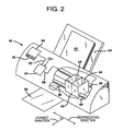
- an inkjet printhead of the present invention is shown generally as 10.
- the printhead 10 has a housing 12 formed of any suitable material for holding ink. Its shape can vary and often depends upon the external device that carries or contains the printhead.
- the housing has at least one compartment 16 internal thereto for holding an initial or refillable supply of ink.
- the compartment has a single chamber and holds a supply of black ink, photo ink, cyan ink, magenta ink or yellow ink.
- the compartment has multiple chambers and contains three supplies of ink.
- it includes cyan, magenta and yellow ink.
- the compartment contains plurals of black, photo, cyan, magenta or yellow ink.
- the compartment 16 is shown as locally integrated within a housing 12 of the printhead, it may alternatively connect to a remote source of ink and receive supply from a tube, for example.
- Adhered to one surface 18 of the housing 12 is a portion 19 of a flexible circuit, especially a tape automated bond (TAB) circuit 20.
- the other portion 21 of the TAB circuit 20 is adhered to another surface 22 of the housing.
- the two surfaces 18, 22 are perpendicularly arranged to one another about an edge 23 of the housing.
- the TAB circuit 20 supports a plurality of input/output (I/O) connectors 24 thereon for electrically connecting a heater chip 25 to an external device, such as a printer, fax machine, copier, photo-printer, plotter, all-in-one, etc., during use.
- I/O input/output
- Pluralities of electrical conductors 26 exist on the TAB circuit 20 to electrically connect and short the I/O connectors 24 to the input terminals (bond pads 28) of the heater chip 25.
- Those skilled in the art know various techniques for facilitating such connections. For simplicity, Figure 1 only shows eight I/O connectors 24, eight electrical conductors 26 and eight bond pads 28 but present day printheads have much larger quantities and any number is equally embraced herein. Still further, those skilled in the art should appreciate that while such number of connectors, conductors and bond pads equal one another, actual printheads may have unequal numbers.
- the heater chip 25 contains a column 34 of a plurality of fluid firing elements that serve to eject ink from compartment 16 during use.
- the fluid firing-elements may embody thermally resistive heater elements (heaters for short) formed as thin film layers on a silicon substrate or piezoelectric elements despite the thermal technology implication derived from the name heater chip.
- the pluralities of fluid firing elements in column 34 are shown as a row of five dots but in practice may include several hundred or thousand fluid firing elements.
- vertically adjacent ones of the fluid firing elements may or may not have a lateral spacing gap or stagger there between.
- the fluid firing elements have vertical pitch spacing comparable to the dots-per-inch resolution of an attendant printer.
- Some examples include spacing of 1/300 th , 1/600 th , 1/1200 th , 1/2400 th or other of an inch (0.085, 0.042, 0.021, 0.0106 mm) along the longitudinal extent of the via.
- many processes are known that cut or etch the via through a thickness of the heater chip. Some of the more preferred processes include grit blasting or etching, such as wet, dry, reactive-ion-etching, deep reactive-ion-etching, or other.
- a nozzle plate (not shown) has orifices thereof aligned with each of the heaters to project the ink during use. The nozzle plate may attach with an adhesive or epoxy or may be fabricated as a silicon thin-film layer.
- an external device in the form of an inkjet printer for containing the printhead 10 is shown generally as 40.
- the printer 40 includes a carriage 42 having a plurality of slots 44 for containing one or more printheads 10.
- the carriage 42 reciprocates (in accordance with an output 59 of a controller 57) along a shaft 48 above a print zone 46 by a motive force supplied to a drive belt 50 as is well known in the art.
- the reciprocation of the carriage 42 occurs relative to a print medium, such as a sheet of paper 52 that advances in the printer 40 along a paper path from an input tray 54, through the print zone 46, to an output tray 56.
- Ink drops from compartment 16 are caused to be ejected from the heater chip 25 at such times pursuant to commands of a printer microprocessor or other controller 57.
- the timing of the ink drop emissions corresponds to a pattern of pixels of the image being printed. Often times, such patterns become generated in devices electrically connected to the controller 57 (via Ext. input) that reside externally to the printer and include, but are not limited to, a computer, a scanner, a camera, a visual display unit, a personal data assistant, or other.
- the fluid firing elements (the dots of column 34, Figure 1 ) are uniquely addressed with a small amount of current to rapidly heat a small volume of ink. This causes the ink to vaporize in a local ink chamber between the heater and the nozzle plate and eject through, and become projected by, the nozzle plate towards the print medium.
- the fire pulse required to emit such ink drop may embody a single or a split firing pulse and is received at the heater chip on an input terminal (e.g., bond pad 28) from connections between the bond pad 28, the electrical conductors 26, the I/O connectors 24 and controller 57.
- Internal heater chip wiring conveys the fire pulse from the input terminal to one or many of the fluid firing elements.
- a control panel 58 having user selection interface 60, also accompanies many printers as an input 62 to the controller 57 to provide additional printer capabilities and robustness.
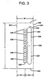
- a heater chip 325 of one embodiment of the present invention has a sole ink via 332 with a longitudinal extent defined by two sides 384, 386.
- a sole column 334 of a plurality of fluid firing elements 335 exists exclusively along one of the two sides of the ink via.
- a chip centroid (+) resides within the sole column 334 external to a boundary 337 of the ink via.
- a via centroid (•) is substantially offset from the chip centroid in the widthwise direction w such that the two centroids do not coexist.
- the heater chip has an asymmetrically disposed ink via and silicon space on a side of the ink via not containing any fluid firing elements is no longer wasted.
- a straight line distance between the chip centroid and the via centroid is about 150 microns.
- a distance from the side 386 to a periphery 339 of the heater chip is about 600 microns which offers about 100 to 300 microns of silicon savings over the prior art.
- the column of fluid firing elements exists substantially centred in the widthwise direction w of the heater chip such that distance D1 is substantially equidistant to distance D2.
- widthwise direction w corresponds to the Reciprocating Direction of Figure 2 .
- the sole ink via 332 is thereby asymmetrically arranged in the Reciprocating Direction.
- an individual heater chip diced from a larger multi-chip wafer will likely embody a rectangular shape in its largest surface area and have two long 341 and short 343 ends as shown.
- a representative lengthwise distance L of the heater chip is about 17 millimeters (mm) while the widthwise distance w is about 3 mm.
- the present invention contemplates other heater chip geometric shapes such as ovals, circles, squares, triangles, polygons or other shapes lending themselves to symmetrical or asymmetrical peripheries or regular or irregular boundaries.
- chip centroid To calculate the chip centroid, well known standard formulas are used. Since the heater chip itself is a three-dimensional (3-D) object, the chip centroid for purposes of this invention can either correspond to the chip centroid of the actual 3-D object or the 2-D figure shown diagrammatically. Likewise, the calculation of the via centroids are governed by standard formulas and may either correspond to the actual 3-D object or the 2-D figure representation.
- the ink vias of the rectangular heater chip can comprise other orientations that remain asymmetrical in the Reciprocating Direction but not in the advance direction
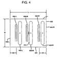
- the heater chip 425 of Figure 4 having lengthwise asymmetrical vias.
- a plurality of ink vias 432-L, 432-M, 432-R are disposed with their lengthwise extents generally parallel to the widthwise direction of the chip.
- none of the via centroids (•) coexist with the chip centroid (+).
- the two rightmost of the ink vias reside closer to the short end 443-R while the leftmost via resides closer to the other of the short ends 443-L.
- all of the ink vias reside substantially equidistant to both of the long ends 441.
- the chip centroid (+) resides between a column 434-M of fluid firing elements and a longitudinal side 484 of the middle ink via 432-M.
- Preferred chip distances include a lengthwise distance of about 8 mm and a widthwise distance of about 5.1 mm. Alternatively, the lengthwise distance is shorter and is about 5.1 mm while the widthwise distance is about 8 mm.
- the leftmost column 434-L of fluid firing elements is about 1.2 mm (D3) from a short end periphery 443-L of the heater chip while the rightmost column 434-R of fluid firing elements is about 1 mm (D4) from the other short end periphery 443-R.
- any given column of fluid firing elements will comprise a plurality of individual fluid firing elements representatively numbered 1 through n ( Figures 5A, 5B ) or numbered 1 through n-1 or 2 through n ( Figure 5C ).
- the fluid firing elements of a given column 534 exist exclusively along one side 584 of an ink via 532, having a longitudinal extent, and have a slight horizontal spacing gap S between vertically adjacent ones of fluid firing elements.
- the spacing gap S is about 3/1200 th of an inch (0.063 mm).
- a vertical distance between vertically adjacent ones is the fluid firing element pitch and generally corresponds to the DPI of the printer in which they are used.
- preferred pitch includes, but is not limited to, 1/300 th , 1/600 th , 1/1200 th , 1/2400 th of an inch (0.085, 0.042, 0.021, 0.0106 mm).
- some of the ink vias of the heater chip may have more than one column of fluid firing elements and both may be disposed on the same side or on opposite sides of the ink via 532 in columns 534-L and 534-R.
- Each column may have a spacing gap S1, S2 between vertically adjacent ones of fluid firing elements or may not.
- spacing gaps S1, S2 are substantially equal.
- Pitch P in this embodiment may be measured between sequentially numbered fluid firing elements such that a twice pitch 2P vertical spacing exists between sequential odd or even numbered fluid firing elements.
- a heater chip 625 can have all pluralities of ink vias 632 disposed asymmetrically closer to a single end of the chip, such as long end 641-R.
- asymmetry can also be described in terms of centroids and none of the ink via centroids (•) resides coincidentally with the chip centroid (+).
- the chip centroid resides at position A between a column of fluid firing elements 634 (shown as a line) and a periphery 637 of the center ink via.
- the column of fluid firing elements is centered in the Reciprocating Direction and the chip centroid (+) resides at position B.
- chip centroids shown in the previous figures all reside external to a boundary of any ink via, the present invention is not so limited to preclude the chip centroid from existing within a boundary of the ink via.
- preferred deposition techniques include, but are not limited to, any variety of chemical vapor depositions (CVD), physical vapor depositions (PVD), epitaxy, evaporation, sputtering or other similarly known techniques.
- CVD techniques include low pressure (LP) ones, but could also include atmospheric pressure (AP), plasma enhanced (PE), high density plasma (HDP) or other.
- Preferred etching techniques include, but are not limited to, any variety of wet or dry etches, reactive ion etches, deep reactive ion etches, etc.
- Preferred photolithography steps include, but are not limited to, exposure to ultraviolet or x-ray light sources, or other, and photomasking includes photomasking islands and/or photomasking holes. The particular embodiment, island or hole, depends upon whether the configuration of the mask is a clear-field or dark-field mask, those terms being well understood in the art.
- the substrate of the heater chip includes a silicon wafer of p-type, 100 orientation, having a resistivity of 5-20 ohm/cm. Its beginning thickness is preferably any one of 525 +/- 20 microns M1.5-89, 625 +/- 20 microns M1.7-89, or 625 +/- 15 microns M1.13-90 with respective wafer diameters of 100 +/-0.50 mm, 125 +/- 0.50 mm, and 150 +/- 0.50 mm.
Landscapes
- Physics & Mathematics (AREA)
- Geometry (AREA)
- Particle Formation And Scattering Control In Inkjet Printers (AREA)
- Ink Jet (AREA)
Claims (12)
- Heizerchip für einen Inkjet-Druckkopf, der zu einer Bewegung in einer Hin- und Her-Richtung in einem Drucker eingerichtet ist, welche eine Vorwärtsrichtung in Bezug auf ein Druckmedium umfasst, mit:einer Chipmitte bzw. einem Chipschwerpunkt (+);einer Säule bzw. Reihe von fluidabschießenden Elementen (334); undeiner einzigen Tintenbohrung (332) mit zwei Seiten (384, 386), welche einer Längsstreckung aufweist; dadurch gekennzeichnet, dass die Reihe fluidabschießender Elemente ausschließlich entlang einer der zwei Seiten existiert und relativ zu dem Heizerchip in Bezug auf die Hin- und Her-Richtung zentriert ist; und wobei ein Bohrungsschwerpunkt der einzigen Tintenbohrung im Wesentlichen zu dem Chipschwerpunkt versetzt ist.
- Heizerchip nach Anspruch 1, wobei der Chipschwerpunkt zwischen der einen der zwei Seiten der einzigen Tintenbohrung und der Reihe fluidabschießender Elemente sitzt.
- Heizerchip nach Anspruch 1, bei dem der Chipschwerpunkt im Wesentlichen innerhalb der Reihe fluidabschießender Elemente sitzt.
- Heizerchip nach Anspruch 1, ferner mit einer Reihe von Eingangsanschlüssen (628), und wobei ein Abstand zwischen der Reihe von Eingangsanschlüssen und der Reihe von fluidabschießenden Elementen 880 Mikron beträgt.
- Heizerchip nach Anspruch 1, bei dem ein Abstand zwischen der anderen Seite der zwei Seiten der einzigen Tintenbohrung und einer Peripherie des Heizerchips 600 Mikron beträgt.
- Heizerchip für einen Inkjet-Druckkopf, der zu einer Bewegung in einer Hin- und Her-Richtung in einem Drucker eingerichtet ist, welche eine Vorwärtsrichtung in Bezug auf ein Druckmedium beinhaltet, mit:einem Chipschwerpunkt (+);einer Anzahl von Reihen von fluidabschießenden Elementen; undeiner Anzahl von Tintenbohrungen, die jeweils einen Bohrungsschwerpunkt aufweisen, und wobei keiner der Bohrungssschwerpunkte mit dem Chipschwerpunkt koexistiert; dadurch gekennzeichnet, dass wenigstens eine der Reihen ausschließlich entlang einer einzigen Seite einer Bohrung aus der Anzahl von Tintenbohrungen existiert und relativ zu dem den Heizerchip in Bezug auf die Hin- und Her-Richtung zentriert ist.
- Heizerchip nach Anspruch 6, bei dem andere der Reihen entlang wenigstens zwei Seiten einer anderen Bohrung aus der Anzahl von Tintenbohrungen existiert.
- Heizerchip nach Anspruch 6 mit:einer Dicke; und wobeidie Anzahl von Reihen von fluidabschießenden Elementen im Wesentlichen parallel zueinander ist; und wobeidie Anzahl von Tintenbohrungen durch die Dicke mit zwei Seiten und einer Längserstreckung angeordnet ist; wobei der Chip ferner eine Reihe von Eingangsanschlüssen aufweist, die im Wesentlichen parallel zu der Anzahl von Reihen von fluidabschießenden Elementen sind.
- Inkjet-Druckkopf für einen Inkjet-Drucker, der sich während der Verwendung in einer Hin- und Her-Richtung in Bezug auf ein Druckmedium bewegt, welches sich in einer Vorwärtsrichtung vorwärts bewegt, mit:einer flexiblen Schaltung (20), die einen I/O-Verbinder (24) und einen elektrischen Leiter (26) trägt; undeinem Heizerchip (25) nach Anspruch 6, mit einem Eingangsanschluss, der elektrisch mit dem elektrischen Leiter und dem I/O-Verbinder verbunden ist.
- Inkjet-Druckkopf nach Anspruch 9, wobei die Tintenbohrung eine Längserstreckung im Wesentlichen parallel mit der Vorwärtsrichtung aufweist.
- Inkjet-Drucker mit dem Inkjet-Druckkopf nach Anspruch 9 oder 10.
- Inkjet-Druckkopf für einen Inkjet-Drucker, der sich während der Verwendung in einer Hin- und Her-Richtung in Bezug auf ein Druckmedium bewegt, welches sich in einer Vorwärtsrichtung voranbewegt, mit:einer Tintenversorgung;einer flexiblen Schaltung (20), die eine Anzahl von I/O-Verbindern (24) und eine Anzahl elektrischer Leiter (26) trägt; undeinem Heizerchip (25) nach Anspruch 4 oder 5, wenn diese von Anspruch 4 abhängen, und miteiner Reihe von Eingangsanschlüssen, die elektrisch mit den Anzahlen von elektrischen Leitern und I/O-Verbindern verbunden sind.
Priority Applications (2)
| Application Number | Priority Date | Filing Date | Title |
|---|---|---|---|
| EP08005907.4A EP1967365B1 (de) | 2002-12-30 | 2003-12-24 | Heizchip mit asymmetrischen Durchgängen für einen Tintenstrahldruckkopf |
| EP10009093A EP2266799A1 (de) | 2002-12-30 | 2003-12-24 | Heizchip mit asymmetrischen Durchgängen für einen Tintenstrahldruckkopf |
Applications Claiming Priority (3)
| Application Number | Priority Date | Filing Date | Title |
|---|---|---|---|
| US334157 | 2002-12-30 | ||
| US10/334,157 US6863381B2 (en) | 2002-12-30 | 2002-12-30 | Inkjet printhead heater chip with asymmetric ink vias |
| PCT/US2003/041274 WO2004060682A1 (en) | 2002-12-30 | 2003-12-24 | Inkjet printhead heater chip with asymmetric ink vias |
Related Child Applications (2)
| Application Number | Title | Priority Date | Filing Date |
|---|---|---|---|
| EP08005907.4A Division EP1967365B1 (de) | 2002-12-30 | 2003-12-24 | Heizchip mit asymmetrischen Durchgängen für einen Tintenstrahldruckkopf |
| EP08005907.4 Division-Into | 2008-03-27 |
Publications (3)
| Publication Number | Publication Date |
|---|---|
| EP1587685A1 EP1587685A1 (de) | 2005-10-26 |
| EP1587685A4 EP1587685A4 (de) | 2007-06-27 |
| EP1587685B1 true EP1587685B1 (de) | 2010-09-08 |
Family
ID=32654948
Family Applications (3)
| Application Number | Title | Priority Date | Filing Date |
|---|---|---|---|
| EP03814965A Expired - Lifetime EP1587685B1 (de) | 2002-12-30 | 2003-12-24 | Heizchip für einen tintenstrahldruckkopf mit asymmetrischen tintendurchgängen |
| EP08005907.4A Expired - Lifetime EP1967365B1 (de) | 2002-12-30 | 2003-12-24 | Heizchip mit asymmetrischen Durchgängen für einen Tintenstrahldruckkopf |
| EP10009093A Withdrawn EP2266799A1 (de) | 2002-12-30 | 2003-12-24 | Heizchip mit asymmetrischen Durchgängen für einen Tintenstrahldruckkopf |
Family Applications After (2)
| Application Number | Title | Priority Date | Filing Date |
|---|---|---|---|
| EP08005907.4A Expired - Lifetime EP1967365B1 (de) | 2002-12-30 | 2003-12-24 | Heizchip mit asymmetrischen Durchgängen für einen Tintenstrahldruckkopf |
| EP10009093A Withdrawn EP2266799A1 (de) | 2002-12-30 | 2003-12-24 | Heizchip mit asymmetrischen Durchgängen für einen Tintenstrahldruckkopf |
Country Status (8)
| Country | Link |
|---|---|
| US (4) | US6863381B2 (de) |
| EP (3) | EP1587685B1 (de) |
| JP (1) | JP2006512236A (de) |
| CN (1) | CN100588544C (de) |
| AU (1) | AU2003303559A1 (de) |
| DE (1) | DE60334151D1 (de) |
| TW (1) | TWI328521B (de) |
| WO (1) | WO2004060682A1 (de) |
Families Citing this family (18)
| Publication number | Priority date | Publication date | Assignee | Title |
|---|---|---|---|---|
| TWI306415B (en) * | 2006-12-19 | 2009-02-21 | Ind Tech Res Inst | Inkjet dispensing apparatus |
| WO2008154672A1 (en) * | 2007-06-19 | 2008-12-24 | Silverbrook Research Pty Ltd | Printhead with heaters offset from nozzles |
| JP2009006562A (ja) * | 2007-06-27 | 2009-01-15 | Canon Inc | インクジェット記録ヘッド |
| US7780271B2 (en) * | 2007-08-12 | 2010-08-24 | Silverbrook Research Pty Ltd | Printhead with heaters offset from nozzles |
| JP2009143140A (ja) * | 2007-12-14 | 2009-07-02 | Canon Inc | インクジェットヘッド |
| US8567912B2 (en) * | 2010-04-28 | 2013-10-29 | Eastman Kodak Company | Inkjet printing device with composite substrate |
| US8672436B2 (en) | 2010-11-02 | 2014-03-18 | Xerox Corporation | Method and system for improved ink jet or printhead replacement |
| CN102689512B (zh) * | 2011-03-23 | 2015-03-11 | 研能科技股份有限公司 | 喷墨头结构 |
| TWI468303B (zh) * | 2011-03-23 | 2015-01-11 | Microjet Technology Co Ltd | 噴墨頭結構 |
| TWI472436B (zh) * | 2011-03-23 | 2015-02-11 | Microjet Technology Co Ltd | 噴墨頭結構 |
| TWI472438B (zh) * | 2011-03-23 | 2015-02-11 | Microjet Technology Co Ltd | 噴墨頭結構 |
| TWI472437B (zh) * | 2011-03-23 | 2015-02-11 | Microjet Technology Co Ltd | 噴墨頭結構 |
| CN103442894B (zh) * | 2011-03-31 | 2016-03-16 | 惠普发展公司,有限责任合伙企业 | 打印头组件 |
| WO2012166112A1 (en) * | 2011-05-31 | 2012-12-06 | Hewlett-Packard Development Company, L.P. | Printhead die |
| US8960860B2 (en) | 2011-04-27 | 2015-02-24 | Hewlett-Packard Development Company, L.P. | Printhead die |
| JP5847444B2 (ja) | 2011-06-07 | 2016-01-20 | キヤノン株式会社 | インクジェットヘッド |
| US9833991B2 (en) | 2014-09-29 | 2017-12-05 | Funai Electric Co., Ltd. | Printhead and an inkjet printer |
| ES2995972T3 (en) * | 2019-02-06 | 2025-02-11 | Hewlett Packard Development Co | Integrated circuits to drive fluid actuation devices |
Family Cites Families (24)
| Publication number | Priority date | Publication date | Assignee | Title |
|---|---|---|---|---|
| GB2113447B (en) * | 1981-12-22 | 1986-07-09 | Casio Computer Co Ltd | Tone signal generating apparatus of electronic musical instruments |
| US4587534A (en) | 1983-01-28 | 1986-05-06 | Canon Kabushiki Kaisha | Liquid injection recording apparatus |
| US4683481A (en) * | 1985-12-06 | 1987-07-28 | Hewlett-Packard Company | Thermal ink jet common-slotted ink feed printhead |
| CA1303904C (en) | 1987-08-10 | 1992-06-23 | Winthrop D. Childers | Offset nozzle droplet formation |
| US4794411A (en) | 1987-10-19 | 1988-12-27 | Hewlett-Packard Company | Thermal ink-jet head structure with orifice offset from resistor |
| JP2642670B2 (ja) | 1988-06-21 | 1997-08-20 | キヤノン株式会社 | インクジェット記録ヘッドの製造方法 |
| JPH0278564A (ja) | 1988-06-30 | 1990-03-19 | Canon Inc | インクジェット記録ヘッドおよびインクジェット記録装置 |
| US5016023A (en) * | 1989-10-06 | 1991-05-14 | Hewlett-Packard Company | Large expandable array thermal ink jet pen and method of manufacturing same |
| US5030971B1 (en) * | 1989-11-29 | 2000-11-28 | Xerox Corp | Precisely aligned mono- or multi-color roofshooter type printhead |
| EP0641654B1 (de) | 1990-04-27 | 1997-07-23 | Canon Kabushiki Kaisha | Aufzeichnungsverfahren und -gerät |
| US5211806A (en) | 1991-12-24 | 1993-05-18 | Xerox Corporation | Monolithic inkjet printhead |
| US5317346A (en) * | 1992-03-04 | 1994-05-31 | Hewlett-Packard Company | Compound ink feed slot |
| US5874974A (en) | 1992-04-02 | 1999-02-23 | Hewlett-Packard Company | Reliable high performance drop generator for an inkjet printhead |
| EP0785072B1 (de) | 1996-01-16 | 2002-04-17 | Canon Kabushiki Kaisha | Tintenstrahlkopf, Tintenstrahlkopfpatrone, Tintenstrahlapparat und Tintenstrahlaufzeichnungsverfahren für Gradationsaufzeichnung |
| JP3403009B2 (ja) | 1996-07-12 | 2003-05-06 | キヤノン株式会社 | 可動部材の変位と気泡成長を伴う液体吐出方法、該吐出方法に用いられる液体吐出ヘッド、ヘッドカートリッジ及びこれらを用いた液体吐出装置 |
| US6220698B1 (en) * | 1996-07-26 | 2001-04-24 | Seiko Epson Corporation | Ink jet type recording head |
| US5818478A (en) | 1996-08-02 | 1998-10-06 | Lexmark International, Inc. | Ink jet nozzle placement correction |
| JP3262009B2 (ja) * | 1997-02-14 | 2002-03-04 | ミノルタ株式会社 | 画像形成装置 |
| US5967208A (en) * | 1997-04-04 | 1999-10-19 | Calvert Manufacturing, Inc. | Method and apparatus for rotary cutting of wood veneer |
| US6019907A (en) * | 1997-08-08 | 2000-02-01 | Hewlett-Packard Company | Forming refill for monolithic inkjet printhead |
| US6042222A (en) | 1997-08-27 | 2000-03-28 | Hewlett-Packard Company | Pinch point angle variation among multiple nozzle feed channels |
| US6428144B2 (en) | 2000-04-04 | 2002-08-06 | Canon Kabushiki Kaisha | Ink jet recording head and inkjet recording apparatus |
| US6267468B1 (en) * | 2000-04-13 | 2001-07-31 | Hewlett-Packard Company | Printhead substrate having a mixture of single and double sided elongate ink feed channels |
| US6443564B1 (en) | 2000-11-13 | 2002-09-03 | Hewlett-Packard Company | Asymmetric fluidic techniques for ink-jet printheads |
-
2002
- 2002-12-30 US US10/334,157 patent/US6863381B2/en not_active Expired - Lifetime
-
2003
- 2003-12-24 CN CN200380108015A patent/CN100588544C/zh not_active Expired - Lifetime
- 2003-12-24 EP EP03814965A patent/EP1587685B1/de not_active Expired - Lifetime
- 2003-12-24 EP EP08005907.4A patent/EP1967365B1/de not_active Expired - Lifetime
- 2003-12-24 EP EP10009093A patent/EP2266799A1/de not_active Withdrawn
- 2003-12-24 DE DE60334151T patent/DE60334151D1/de not_active Expired - Lifetime
- 2003-12-24 WO PCT/US2003/041274 patent/WO2004060682A1/en not_active Ceased
- 2003-12-24 JP JP2004565708A patent/JP2006512236A/ja active Pending
- 2003-12-24 AU AU2003303559A patent/AU2003303559A1/en not_active Abandoned
- 2003-12-30 TW TW092137493A patent/TWI328521B/zh not_active IP Right Cessation
-
2004
- 2004-09-22 US US10/946,679 patent/US7077509B2/en not_active Expired - Lifetime
- 2004-09-22 US US10/946,680 patent/US7014299B2/en not_active Expired - Lifetime
-
2005
- 2005-11-08 US US11/269,311 patent/US7244015B2/en not_active Expired - Lifetime
Also Published As
| Publication number | Publication date |
|---|---|
| EP1967365A3 (de) | 2008-12-17 |
| US6863381B2 (en) | 2005-03-08 |
| CN100588544C (zh) | 2010-02-10 |
| DE60334151D1 (de) | 2010-10-21 |
| US20060055738A1 (en) | 2006-03-16 |
| TW200422194A (en) | 2004-11-01 |
| WO2004060682B1 (en) | 2004-10-07 |
| EP1587685A4 (de) | 2007-06-27 |
| US7014299B2 (en) | 2006-03-21 |
| US7244015B2 (en) | 2007-07-17 |
| EP1587685A1 (de) | 2005-10-26 |
| EP1967365B1 (de) | 2014-09-24 |
| US7077509B2 (en) | 2006-07-18 |
| US20050041072A1 (en) | 2005-02-24 |
| US20040125173A1 (en) | 2004-07-01 |
| JP2006512236A (ja) | 2006-04-13 |
| EP1967365A2 (de) | 2008-09-10 |
| AU2003303559A1 (en) | 2004-07-29 |
| TWI328521B (en) | 2010-08-11 |
| CN1732088A (zh) | 2006-02-08 |
| WO2004060682A1 (en) | 2004-07-22 |
| EP2266799A1 (de) | 2010-12-29 |
| HK1088283A1 (zh) | 2006-11-03 |
| US20050041071A1 (en) | 2005-02-24 |
Similar Documents
| Publication | Publication Date | Title |
|---|---|---|
| EP1587685B1 (de) | Heizchip für einen tintenstrahldruckkopf mit asymmetrischen tintendurchgängen | |
| US7669978B2 (en) | Inkjet printhead packaging tape for sealing nozzles | |
| US6866790B2 (en) | Method of making an ink jet printhead having a narrow ink channel | |
| US7090340B2 (en) | Inkjet recording head and inkjet recording apparatus using the same | |
| CA2512165A1 (en) | Heater chip with doped diamond-like carbon layer and overlying cavitation layer | |
| US6764163B2 (en) | Heater configuration for tri-color heater chip | |
| CA2520188C (en) | Inkjet printhead having convex wall bubble chamber | |
| US20080062216A1 (en) | Actuator chip for micro-fluid ejection device with temperature sensing and control per chip zones | |
| CA2641214A1 (en) | Inkjet actuator substrate having at least one non-uniform ink via | |
| US7938508B2 (en) | Low profile printhead | |
| HK1088283B (en) | Inkjet printhead heater chip with asymmetric ink vias | |
| MX2008009958A (en) | Inkjet actuator substrate having at least one non-uniform ink via |
Legal Events
| Date | Code | Title | Description |
|---|---|---|---|
| PUAI | Public reference made under article 153(3) epc to a published international application that has entered the european phase |
Free format text: ORIGINAL CODE: 0009012 |
|
| 17P | Request for examination filed |
Effective date: 20050801 |
|
| AK | Designated contracting states |
Kind code of ref document: A1 Designated state(s): AT BE BG CH CY CZ DE DK EE ES FI FR GB GR HU IE IT LI LU MC NL PT RO SE SI SK TR |
|
| AX | Request for extension of the european patent |
Extension state: AL LT LV MK |
|
| DAX | Request for extension of the european patent (deleted) | ||
| RBV | Designated contracting states (corrected) |
Designated state(s): DE FR GB |
|
| A4 | Supplementary search report drawn up and despatched |
Effective date: 20070529 |
|
| 17Q | First examination report despatched |
Effective date: 20071001 |
|
| GRAP | Despatch of communication of intention to grant a patent |
Free format text: ORIGINAL CODE: EPIDOSNIGR1 |
|
| GRAS | Grant fee paid |
Free format text: ORIGINAL CODE: EPIDOSNIGR3 |
|
| GRAA | (expected) grant |
Free format text: ORIGINAL CODE: 0009210 |
|
| AK | Designated contracting states |
Kind code of ref document: B1 Designated state(s): DE FR GB |
|
| REG | Reference to a national code |
Ref country code: GB Ref legal event code: FG4D |
|
| REF | Corresponds to: |
Ref document number: 60334151 Country of ref document: DE Date of ref document: 20101021 Kind code of ref document: P |
|
| PLBE | No opposition filed within time limit |
Free format text: ORIGINAL CODE: 0009261 |
|
| STAA | Information on the status of an ep patent application or granted ep patent |
Free format text: STATUS: NO OPPOSITION FILED WITHIN TIME LIMIT |
|
| 26N | No opposition filed |
Effective date: 20110609 |
|
| GBPC | Gb: european patent ceased through non-payment of renewal fee |
Effective date: 20101224 |
|
| REG | Reference to a national code |
Ref country code: FR Ref legal event code: ST Effective date: 20110831 |
|
| REG | Reference to a national code |
Ref country code: DE Ref legal event code: R097 Ref document number: 60334151 Country of ref document: DE Effective date: 20110609 |
|
| PG25 | Lapsed in a contracting state [announced via postgrant information from national office to epo] |
Ref country code: FR Free format text: LAPSE BECAUSE OF NON-PAYMENT OF DUE FEES Effective date: 20110103 |
|
| REG | Reference to a national code |
Ref country code: DE Ref legal event code: R119 Ref document number: 60334151 Country of ref document: DE Effective date: 20110701 |
|
| PG25 | Lapsed in a contracting state [announced via postgrant information from national office to epo] |
Ref country code: GB Free format text: LAPSE BECAUSE OF NON-PAYMENT OF DUE FEES Effective date: 20101224 Ref country code: DE Free format text: LAPSE BECAUSE OF NON-PAYMENT OF DUE FEES Effective date: 20110701 |