EP1584375B1 - Dynamically controllable biological/chemical detectors having nanostructured surfaces - Google Patents
Dynamically controllable biological/chemical detectors having nanostructured surfaces Download PDFInfo
- Publication number
- EP1584375B1 EP1584375B1 EP05251553A EP05251553A EP1584375B1 EP 1584375 B1 EP1584375 B1 EP 1584375B1 EP 05251553 A EP05251553 A EP 05251553A EP 05251553 A EP05251553 A EP 05251553A EP 1584375 B1 EP1584375 B1 EP 1584375B1
- Authority
- EP
- European Patent Office
- Prior art keywords
- containment surface
- nanostructured
- droplet
- passing
- projections
- Prior art date
- Legal status (The legal status is an assumption and is not a legal conclusion. Google has not performed a legal analysis and makes no representation as to the accuracy of the status listed.)
- Expired - Lifetime
Links
Images


Classifications
-
- B—PERFORMING OPERATIONS; TRANSPORTING
- B01—PHYSICAL OR CHEMICAL PROCESSES OR APPARATUS IN GENERAL
- B01L—CHEMICAL OR PHYSICAL LABORATORY APPARATUS FOR GENERAL USE
- B01L3/00—Containers or dishes for laboratory use, e.g. laboratory glassware; Droppers
- B01L3/50—Containers for the purpose of retaining a material to be analysed, e.g. test tubes
- B01L3/508—Containers for the purpose of retaining a material to be analysed, e.g. test tubes rigid containers not provided for above
- B01L3/5088—Containers for the purpose of retaining a material to be analysed, e.g. test tubes rigid containers not provided for above confining liquids at a location by surface tension, e.g. virtual wells on plates, wires
-
- B—PERFORMING OPERATIONS; TRANSPORTING
- B01—PHYSICAL OR CHEMICAL PROCESSES OR APPARATUS IN GENERAL
- B01L—CHEMICAL OR PHYSICAL LABORATORY APPARATUS FOR GENERAL USE
- B01L3/00—Containers or dishes for laboratory use, e.g. laboratory glassware; Droppers
- B01L3/50—Containers for the purpose of retaining a material to be analysed, e.g. test tubes
- B01L3/508—Containers for the purpose of retaining a material to be analysed, e.g. test tubes rigid containers not provided for above
-
- B—PERFORMING OPERATIONS; TRANSPORTING
- B01—PHYSICAL OR CHEMICAL PROCESSES OR APPARATUS IN GENERAL
- B01L—CHEMICAL OR PHYSICAL LABORATORY APPARATUS FOR GENERAL USE
- B01L2300/00—Additional constructional details
- B01L2300/08—Geometry, shape and general structure
- B01L2300/089—Virtual walls for guiding liquids
-
- B—PERFORMING OPERATIONS; TRANSPORTING
- B01—PHYSICAL OR CHEMICAL PROCESSES OR APPARATUS IN GENERAL
- B01L—CHEMICAL OR PHYSICAL LABORATORY APPARATUS FOR GENERAL USE
- B01L2300/00—Additional constructional details
- B01L2300/16—Surface properties and coatings
- B01L2300/161—Control and use of surface tension forces, e.g. hydrophobic, hydrophilic
-
- B—PERFORMING OPERATIONS; TRANSPORTING
- B01—PHYSICAL OR CHEMICAL PROCESSES OR APPARATUS IN GENERAL
- B01L—CHEMICAL OR PHYSICAL LABORATORY APPARATUS FOR GENERAL USE
- B01L2400/00—Moving or stopping fluids
- B01L2400/04—Moving fluids with specific forces or mechanical means
- B01L2400/0403—Moving fluids with specific forces or mechanical means specific forces
- B01L2400/0406—Moving fluids with specific forces or mechanical means specific forces capillary forces
-
- B—PERFORMING OPERATIONS; TRANSPORTING
- B01—PHYSICAL OR CHEMICAL PROCESSES OR APPARATUS IN GENERAL
- B01L—CHEMICAL OR PHYSICAL LABORATORY APPARATUS FOR GENERAL USE
- B01L2400/00—Moving or stopping fluids
- B01L2400/04—Moving fluids with specific forces or mechanical means
- B01L2400/0403—Moving fluids with specific forces or mechanical means specific forces
- B01L2400/0415—Moving fluids with specific forces or mechanical means specific forces electrical forces, e.g. electrokinetic
- B01L2400/0421—Moving fluids with specific forces or mechanical means specific forces electrical forces, e.g. electrokinetic electrophoretic flow
-
- B—PERFORMING OPERATIONS; TRANSPORTING
- B01—PHYSICAL OR CHEMICAL PROCESSES OR APPARATUS IN GENERAL
- B01L—CHEMICAL OR PHYSICAL LABORATORY APPARATUS FOR GENERAL USE
- B01L2400/00—Moving or stopping fluids
- B01L2400/04—Moving fluids with specific forces or mechanical means
- B01L2400/0403—Moving fluids with specific forces or mechanical means specific forces
- B01L2400/0415—Moving fluids with specific forces or mechanical means specific forces electrical forces, e.g. electrokinetic
- B01L2400/0427—Electrowetting
-
- B—PERFORMING OPERATIONS; TRANSPORTING
- B01—PHYSICAL OR CHEMICAL PROCESSES OR APPARATUS IN GENERAL
- B01L—CHEMICAL OR PHYSICAL LABORATORY APPARATUS FOR GENERAL USE
- B01L2400/00—Moving or stopping fluids
- B01L2400/04—Moving fluids with specific forces or mechanical means
- B01L2400/0403—Moving fluids with specific forces or mechanical means specific forces
- B01L2400/0433—Moving fluids with specific forces or mechanical means specific forces vibrational forces
- B01L2400/0436—Moving fluids with specific forces or mechanical means specific forces vibrational forces acoustic forces, e.g. surface acoustic waves [SAW]
Definitions
- the present invention relates generally to biological/chemical detectors and, more particularly, to dynamically controllable integrated biological/chemical detectors having nanostructured surfaces.
- Biological and chemical detector technology has become ever more important over the last several years and, as a result, has been undergoing dramatic growth. This growth is primarily fueled by the need for fast, highly sensitive and highly specific detector systems that would reduce false alarm rates and increase the ability to detect and identify chemical and biological species, such as chemical and biological warfare agents, in a wide range of environments.
- chemical and biological agent detection systems rely on separate components or devices for sample collection, separation, and analysis. Thus, operation of such systems often requires multiple manual steps to accomplish, for example, sample preparation and loading, tag and assay handling, fluids recharging, results characterization, etc. None of the commercially available traditional chemical/biological detection systems provides a truly portable integrated unit capable of fully automated detection of multiple chemical or biological agents in a wide range of environments.
- LabChip® system produced by Caliper Technologies, uses chips having small channels e.g from 5 micrometers to 50 micrometers to control the flow of samples across a surface for analysis.
- the chips in the Caliper Technologies system are inserted into the LabChip® system, which includes multiple components for containing reagents and software for controlling experiments and displaying results.
- the LabChip® system reduces the number of manual steps, thus reducing human error, and requires very small levels of reagent to operate.
- LILLIPUT chip which is used, for example, with microParts Corporation microspectrometer, uses microchannels linked to a large number of sampling wells in a very small package. Once again, after pipette samples are introduced onto the chip, the samples are routed to the appropriate sampling well via microchannel. As in the LabChip® system, other components are used to analyze the samples and display the results of the analysis.
- samples are electrically directed along the surface of a chip to one of a number of test sites.
- the samples in the NanoChipTM system can be attracted to a particular test site by creating an opposite charge at that test site.
- a negatively-charged sample is introduced into the NanoChipTM system, e.g., via pipette, that sample can be directed to one or more positively charged test sites.
- microfluidics-based systems achieve a certain amount of integration over such traditional systems, such microfluidics-based systems still typically lack full integration of components. Therefore, for example, such systems require separate components to analyze the samples and characterize the results of the analysis. Also, such microfluidics systems are typically characterized by relatively low sample throughput, relatively low component integration density, poor reliability, and often require substantial power to generate effective liquid flow actuation. Therefore, the present inventors have invented an integrated, dynamically controllable biological/chemical detector that is capable of manipulating liquids, such as reagent droplets, across nanostructured surfaces without relying on microchannels.
- a detector for detecting the presence of a particle in a fluid flow, the detector including a first containment surface, and a second containment surface substantially parallel to and spaced apart from the first containment surface.
- the second containment surface has a plurality of nanostructured projections disposed in an array of reagent pixels thereon, the nanostructured projections having tips.
- At least a first reagent pixel in said array of reagent pixels has at least a first reagent disposed on the second containment surface between said nanostructured projections.
- the detector includes means for passing a fluid flow including a particle through the first containment surface.
- the detector also includes means for passing the fluid flow through the second containment surface in a way such that a first size of a particle is prevented from passing through the second containment surface.
- the detector includes a plurality of electrodes disposed on said second containment surface.
- the detector further includes a voltage source for sequentially applying a voltage to said electrodes in a way such that a liquid droplet formed on a plurality of said tips can be moved across said plurality of tips to said first reagent pixel.
- the detector also includes means for causing a liquid droplet on a plurality of said tips to penetrate the nanostructured projections causing a particle to reach said second containment surface in at least the first reagent pixel to contact said first reagent.
- a method for detecting a particle contained in a flow of a fluid passed through a detector, the detector including a first containment surface, the detector including a second containment surface substantially parallel to and spaced apart from the first containment surface, the second containment surface having a plurality of nanostructured projections disposed in an array of reagent pixels thereon, the nanostructured projections having tips.
- the method includes passing a fluid flow containing particles through the first containment surface, and passing the fluid flow through the second containment surface in a way such that a first size of a particle is prevented from passing through the second containment surface.
- the method includes collecting particles from the fluid flow on the nanostructured projections of the second containment surface.
- the method further includes forming a liquid droplet on tips of a plurality of nanostructured projections disposed on the second containment surface, the liquid droplet being adapted to absorb particles introduced into the detector by the fluid flow.
- the method also includes moving the liquid droplet over a portion of the tips of said nanostructured projections in a way such that said liquid droplet reaches a selected pixel on said second containment surface, the pixel having a reagent disposed on the second containment surface.
- the method additionally includes penetrating said liquid droplet between nanostructured projections, carrying a particle to the reagent at the selected pixel. Penetrating said liquid droplet between nanostructured projections on said selected pixel generates at least a first indication as to whether or not a particle of a particular biological species or chemical compound is disposed in said fluid flow.
- Figures 1-3 and 9 illustrate the prior art.
- Figures 4-8 illustrate principles that may be utilized in implementations of the invention as are shown in Figures 10-18 .
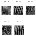
- FIGS. 1A 1E show different illustrative superhydrophobic surfaces produced using various methods. Specifically, these figures show surfaces having small posts, known as nanoposts and/or microposts with various diameters and with different degrees of regularity.
- An illustrative method of producing nanoposts and microposts found in U.S. Pat. No. 6,185,961 , titled “Nanopost arrays and process for making same," issued Fcb. 13, 2001 to Tonucci, et al,. Nanoposts have been manufactured by various methods, such as by using a template to form the posts, by various means of lithography, and by various methods of etching.
- the Kim reference teaches that, by finely patterning the surface in contact with the liquid, and using the aforementioned principle of liquid surface tension, a droplet of liquid disposed on the surface will be supported on the tops of the nanostructure pattern, as shown in FIG. 2 .
- droplet 201 of an appropriate liquid depending upon the surface structure
- This results in an extremely low area of contact between the droplet and the surface 202 i.e., the droplet only is in contact with the top of each post 203) and, hence a low flow resistance.
- FIGs 3A-3F show how different, extremely fine-featured microstructure and nanostructure surface patterns result in different contact angles between the resulting surface and a droplet of liquid.
- FIGs. 3A and 3B show a microline surface and a micropost surface, respectively.
- Each of the lines 301 in FIG. 3A is approximately 3-5 micrometers in width and each of the microposts 302 in FIG. 3B is approximately 3-5 micrometers in diameter at its widest point. Comparing the microline pattern to the micropost pattern, for a given size droplet disposed on each of the surfaces, the contact area of the droplet with the microline pattern will be greater than the contact area of the droplet with the micropost pattern.
- 3D and 3E show the contact angle of a droplet relative to the microline surface of FIG. 3A and the micropost surface of FIG. 3B , respectively.
- the contact angle 303 of the droplet 305 on the microline pattern is smaller (-150 degrees) than the contact angle 304 of the droplet 306 with the micropost pattern ( ⁇ 160 degrees). As described above, it directly follows that the flow resistance exerted on the droplet by the microline pattern will be higher than that exerted by the micropost pattern.
- FIG. 3C shows an even finer pattern than that of the microline and micropost pattern.
- FIG. 3C shows a nanopost pattern with each nanopost 309 having a diameter of less than 1 micrometer. While FIG. 3C shows nanoposts 309 formed in a somewhat conical shape, other shapes and sizes are also achievable. In fact, cylindrical nanopost arrays have been produced with each nanopost having a diameter of less than 10 nm.
- a droplet 307 disposed on the nanopost surface of FIG. 3C is nearly spherical with a contact angle 308 between the surface and the droplet equal to between 175 degrees and 180 degrees. The droplet 307 disposed on this surface experiences nearly zero flow resistance.
- FIGs. 4A and 4B show one embodiment in accordance with the principles of the present invention where electrowetting is used to control the penetration of a liquid into a nanostructured surface.
- electrowetting is the subject of copending US Patent Application, Serial Number 10/403159, filed 03/31/2003 , and titled "Method and Apparatus for Controlling the Movement of a Liquid on a Nanostructured or Microstructured Surface.
- a droplet 401 of conducting liquid is disposed on a nanostructure feature pattern of conical nanoposts 402, as described above, such that the surface tension of the droplet 401 results in the droplet being suspended on the upper portion of the nanoposts 402.
- the droplet only covers surface area f 1 of each nanopost.
- the nanoposts 402 are supported by the surface of a conducting substrate 403.
- Droplet 401 is illustratively electrically connected to substrate 403 via lead 404 having voltage source 405.
- An illustrative nanopost is shown in greater detail in FIG. 5 .
- nanopost 402 is electrically insulated from the liquid (401 in FIG. 9A) by material 501, such as an insulating layer of dielectric material.
- the nanopost is further separated from the liquid by a low surface energy material 502, such as a well-known fluoropolymer.
- a low surface energy material 502 allows one to obtain an appropriate initial contact angle between the liquid and the surface of the nanopost. It will be obvious to one skilled in the art that, instead of using two separate layers of different material, a single layer of material that possesses sufficiently low surface energy and sufficiently high insulating properties could be used.
- FIG. 4B shows that by, for example, applying a low voltage (e.g., 10 - 20 volts) to the conducting droplet of liquid 401, a voltage difference results between the liquid 401 and the nanoposts 402.
- a low voltage e.g. 10 - 20 volts
- the contact angle between the liquid and the surface of the nanopost decreases and, at a sufficiently low contact angle, the droplet 401 moves down in the y-direction along the surface of the nanoposts 402 and penetrates the nanostructure feature pattern until it complete surrounds each of the nanoposts 402 and comes into contact with the upper surface of substrate 403.
- the droplet covers surface area f 2 of each nanopost.
- the droplet 401 effectively becomes stationary relative to the nanostructure feature pattern in the absence of another force sufficient to dislodge the droplet 401 from the feature pattern.
- Other methods of causing the above-described penetration of the nanostructured feature pattern may also be used, such as, for example, increasing the temperature of the droplet or the nanostructures, altering the chemical composition of the droplet, or using acoustic or radio frequency waves to reduce the surface tension of the droplet.
- One skilled in the art will be able to devise alternate methods of causing penetration of the droplet into the nanostructured feature pattern in light of the teachings herein.
- FIGs. 6A and 6B show an embodiment of a biological or chemical detector, as described in the aforementioned copending '159 application, that uses the nanostructured feature pattern represented in FIG. 4 .
- droplet 601 is disposed on nanostructures 602 similar to that shown in FIG. 4A .
- Detectors 606, which are able to detect the desired biological or chemical compound 603, are illustratively disposed on surface 604.
- the liquid for droplet 601 and the nanostructures 602 are chosen such that, for example, when the desired compound 603 enters the liquid in a desired amount, the surface tension of the liquid drops and, as shown in FIG. 6B , the liquid 601 penetrates the nanostructure pattern and comes into contact with the detectors 606.
- droplet could be caused to penetrate the nanostructures using the above-discussed electrowetting method.
- an indication of such contact can be generate by well-known methods, such as via the generating of an electrical signal or the changing of the color of the detector.
- FIGs. 6A and 6B may also be used as a method of achieving a desired chemical reaction.
- a liquid for droplet 601 such that the liquid already contains a compound 603, such as a chemical compound or a biological agent, such as antigens, antibodies, DNA, RNA or other various biologically active species such as RNA polymerase DNA transcriptase, etc.
- Detectors 606 in this embodiment are fashioned out of a desired reactant compound that will achieve a desired reaction when in contact with element or compound 603.
- detectors/reactants 606 are disposed between the nanostructures such that, when the liquid droplet penetrates the nanostructure feature pattern as shown in FIG. 6B , the two or more chemicals or species come into contact with each other and the desired reaction occurs.
- the droplet can be made to penetrate the feature pattern by either applying a voltage to the droplet or, alternatively, by using some method for lowering the surface tension of the liquid droplet 601 (and, thus, the contact angle it forms with the surfaces of the nanostructures) such as, for example, increasing the temperature of the liquid droplet 601.
- FIG. 7 shows a possible arrangement of the illustrative embodiments of FlGs. 6A and 6B, whether used as a chemical/biological detector or used in a chemical reaction application.
- a liquid can be made to flow in direction 701 across the surface of array 702, which has a predetermined arrangement of nanostructures patterned on its surface.
- Each of areas 703 may, for example, have detectors/reactants (such as 606 in FIGs. 6A and 6B ) disposed between the nanostructures that are suited, for example, for detecting or reacting with one or more chemical/biological compounds or agents.
- the array 702 of FIG. 7 could be used to detect multiple different compounds.
- each of the areas could be designed so as to react with only a certain compound to achieve the desired reactions.
- FIG. 8 shows a device to accomplish such predetermined movement whereby the nanostructures (nanoposts 802 in this illustrative embodiment) are arranged such that the droplet 801 moves laterally in the x-direction 804. Specifically, the nanoposts 802 are arranged so that the density of nanoposts 802 increases in the x-direction 804. This increased density will lead to a lower contact angle at the leading edge 805 of the droplet relative to the contact angle at the trailing edge 806 of the droplet.
- the lower contact angle at edge 805 leads to a lower force in the x-direction applied to the droplet 801 than does the relatively higher contact angle at edge 806.
- this imbalance of forces will cause the droplet 801 to "drift" in the x-direction 804 toward the area of higher density of nanoposts 802 as the liquid droplet 801 attempts to achieve equilibrium.
- a liquid droplet can be initially disposed at another location on the surface and it will autonomously move toward that area of highest density of nanoposts. This and other methods of causing a droplet to move laterally across a nanostructured surface are described in the copending '159 Application.
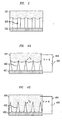
- FIG. 9 shows a prior art embodiment of a structure 901 that relies on the electrowetting principles as opposed to different densities of nanostructures, as described above, to move a droplet of conductive fluid 902 across substrate 909 that is, for example, one of two rigid hydrophobic substrates 909 and 910 disposed parallel to each other.
- the second rigid substrate 910 on top of droplet 902 constrains the movement of the droplet in the y-direction.
- Layers 906a and 906b which are illustrative insulating surfaces, are disposed on a first surface of substrate 909 and first surface of substrate layer 910, respectively.
- Dielectric layer 915 serves to separate two electrodes, 904 and 905 respectively, from the layer 906a and droplet 902.
- the dielectric layer is, for example, a 6 ⁇ m thick layer of polyimide. Electrodes 904 and 905 are separated from each other by a dielectric spacer 911 such as, e.g., a spacer made from Teflon® material manufactured by Dupont or, alternatively, simply a gap between the electrodes.
- a third unpatterned ground electrode 908 is disposed on substrate 910 in a way such that it is not in contact with either electrodes 904 or 905.
- the inner surfaces 906a and 906b are, for example, hydrophobic surfaces, such as surfaces manufactured from a well-known fluoropolymer.
- Electrowetting principles are used to reversibly change the contact angle ⁇ between the liquid and the inner surface 906a.
- ⁇ 1 is determined by the interfacial tensions ⁇ as explained above.
- V a voltage applied to the electrode 905
- the voltage difference between the electrode 905 and the droplet 902 causes the droplet to attempt to spread.
- the contact angle where boundary 913 meets surface 909 decreases when the voltage is applied between the electrode 905 and the droplet 902.
- the voltage V necessary to achieve this change may range from several volts to several hundred volts.
- the amount of movement i.e., as determined by the difference between ⁇ 1 and ⁇ 2 , is a function of the applied voltage V.
- ⁇ 1 is the contact angle between the surface 906a and the droplet 902 when no voltage is applied between the droplet 902 and electrode 905
- ⁇ L-V is the droplet interfacial tension
- ⁇ r is the dielectric constant of the layer 906a
- ⁇ 0 is 8.85 x 10 -12 F/M - the permittivity of a vacuum. Since the droplet of FIG.
- FIG. 10 shows an integrated biological/chemical detector in accordance with the principles of the present invention whereby, for example, airborne chemical and/or biological particles are collected and transported to specific pixels in a detector array. The particles are then caused to come into contact with one or more detector reagents in those pixels, thus inducing a chemical reaction. These chemical reactions may cause, for example, the reflectivity of a particular pixel to change or an electrical signal to be generated, thus providing a readily discernible indication for determining whether an airborne particle was detected.
- One skilled in the art will appreciate in light of the teachings herein below that, while the embodiments herein describe particles in an airflow, those embodiments are equally advantageously used with any fluid flow carrying particles, such as a flow of a liquid.
- detector 1000 is shown having two substantially parallel containment surfaces 1001 and 1002.
- containment surfaces are, illustratively, the inner surfaces of a portable biological/chemical detector, however, any arrangement whereby two surfaces are disposed in a substantially parallel manner are intended to be encompassed by the teachings of the present invention.
- Surfaces 1001 and 1002 are, illustratively, nanostructured surfaces having a plurality of nanostructures similar to the nanostructured surfaces discussed above.
- surface 1001 may or may not be nanostructured depending upon the implementation of the principles disclosed herein.
- Each of surfaces 1001 and 1002 have openings 1003 and 1004, respectively, for allowing a fluid, such as air flow 1005 moving in direction 1006, to enter into the space between the two surfaces 1001 and 1002 and to exit from that space through opening area 1004 as air flow 1009.
- Opening areas 1003 and 1004 may be, illustratively, filtered openings so that only particles below a certain size are permitted to enter the space between the two surfaces 1001 and 1002.
- Area 1014 of surface 1002 is, illustratively, a pixilated area wherein some or all of the pixels are capable of holding a pixel reagent.
- the pixel reagents are selected such that, when a pixel reagent comes into contact with a particular substance or element, a desired reaction occurs.
- One skilled in the art will recognize that such an arrangement is useful, for example, in causing a reaction between a pixel reagent and a biological substance.
- the presence of a particular biological or chemical substance can be detected by noting the reaction with the appropriate pixilated reagent.
- FIG. 11 shows one illustrative embodiment of how air may enter the volume between surfaces 1001 and 1002 in detector 1000 of FIG. 10 and introduce aerosol particles for collection and sampling by the detector.
- FIG. 11 shows a cross section view of opening areas 1003 and 1004 in FIG. 10 .
- Opening area 1003 has, illustratively, holes 1102 through nanostructured surface 1001 through which air flow 1005 may enter the space 1106 between the surfaces 1001 and 1002.
- illustrative particles 1101 carried by the airflow 1005 also reach area 1003.
- the holes in area 1003 are sized such that larger particles are unable to pass through the holes.
- Nanostructures 1108 are separated from nanostructures 1009 by, for example, 1 to 500 micrometers.
- a number of appropriate separation distances can be chosen.
- Detector 1000 has, for example, a plurality of reagents 1007a, 1007b, 1007c, and 1007d disposed in area 1008. Once particles have been collected on the nanostructures in area 1004, as described above, one or more of the reagents are caused to pass across the nanostructures in area 1004 using methods such as those discussed below.
- reagent droplet 1007a moves across area 1004
- the electrostatic attraction force holding the particles collected on the tips of the nanoposts is overcome by the surface tension force experienced by the particles as they are wetted by the droplet and those particles are absorbed by the reagent droplet 1007a.
- FIG. 12 shows one such method of moving the reagent across the area 1004 between surfaces 1001 and 1002.
- nanostructures on parallel surfaces such as surfaces 1001 and 1002 are separated by a distance h of approximately 200 micrometers.
- Droplet 1007a which, as shown in FIG. 10 is a droplet of reagent, is approximately 100 nanoliters in volume.
- the density of the nanoposts on area 1003 and 1004 in FIG. 10 can illustratively be varied in a way such that, once released from area 1008 in FIG. 10 , reagent droplet 1007a moves in direction 1202 across the nanostructured surfaces 1001 and 1002.
- droplet 1007a moves in predetermined direction 1202. Using the exemplary dimensions described above, it is illustratively possible to move droplet 1007a approximately 50 mm when surfaces 1001 and 1002 are disposed horizontally or approximately 10 mm when surfaces 1001 and 1002 are arranged vertically.
- FIG. 13 shows another illustrative embodiment in accordance with the principles of the present invention whereby a droplet, such as a droplet 1007a of reagent, is caused to move across a surface, such as area 1004 of surface 1002.
- a droplet such as a droplet 1007a of reagent
- FIG. 13 shows illustrative surfaces 1001 and 1002 having a plurality of nanostructured electrodes 1302-1305 disposed thereon.
- droplet 1107a once again is a 100 nanoliter droplet of, for example, reagent and the nanostructures 1108 and 1109 are separated by a distance of approximately 200 micrometers.
- the nanostructures 1108 and 1109 are separated from adjacent nanostructures on the same surface by approximately 1.25 micrometers. Similar to the case discussed in association with FIG.
- the contact angle ⁇ 1 decreases relative to the contact angle ⁇ 2 which corresponds to that portion of the droplet disposed on electrodes 1305 and 1304.
- the droplet 1007a moves, for example, in direction 1301.
- a continuous movement of droplet 1007a may be achieved by sequentially applying and removing the voltages applied to the electrodes, such as electrodes 1302 - 1305 along the desired line of travel of droplet 1007a.
- relatively complex and non-predetermined paths of motion of the droplet 1007a can be achieved across surface 1002 of detector 1000 in FIG. 10 by activating sequentially the electrodes along the path of travel of droplet 1007a.
- droplet 1007a can be made to move using this sequential voltage method in direction 1018 across area 1004, thus collecting aerosol particles collected on the tips of the nanostructures in area 1004.
- the droplet can be made to move across area 1014 of surface 1001 in direction 1010.
- the electrodes along path 1012 and 1016 are sequentially activated, thus causing the droplet to follow path 1012 and path 1016 until the droplet reaches pixel destination 1015. Since the droplet is moving over the nanostructures along surface 1002, neither the droplet nor the aerosol particles absorbed by the droplet come into contact with any reagents along the path of the droplet such as, for example, that reagent in pixel 1017.
- no microchannels are required to move the droplet of liquid to a desired reagent pixel - the movement may be achieved on a planar surface of nanostructures according to the principles described above.
- the voltage applied to the electrodes to achieve motion of the droplet in direction 1301 is selected from the range of voltages below the voltage threshold necessary to overcome the surface tension of the droplet that would cause such penetration. For example, using the dimensions for the droplet and the nanostructured surfaces of FIG. 13 , a voltage of approximately 18 volts would be sufficient to initiate motion of the droplet without causing droplet penetration.
- a range of voltages could be used to achieve this movement without causing penetration, depending upon the dimensions of the nanostructured surfaces and the dimensions and substance used for the droplet.
- FIGs. 14A and 14B show how, as discussed above, a droplet moving along area 1004 of surface 1002 will absorb aerosol particles adhering to the tips of nanostructures 1109.
- the droplet moves via one of the previously-described methods or any other method of motion, as the droplet 1007a moves across the nanostructures 1108 and 1109 of surfaces 1001 and 1002, respectively, the particles adhering to the tips of the nanostructures 1109 in area 1004 become absorbed by the droplet 1007a. Accordingly, as the droplet moves in direction 1401 along the nanostructures, it will carry those absorbed particles 1103.
- a particular location such as pixel 1015 in FIG.
- the droplet may be caused to penetrate the nanostructures using the previously discussed electrowetting penetration, for example, by applying a voltage to the droplet or nanostructures in a way such that the contact angle of the droplet relative to the nanostructures is decreased, thus overcoming the surface tension of the droplet and causing it to penetrate the surface.
- the spacing of nanostructures 1109 may be selected such that, when the droplet penetrates those nanostructures, only the smaller particles within the droplet are permitted to come into contact with surface 1002 where, for example, a reagent 1403 is disposed.
- Reagent 1403 for example, a reagent selected to detect the presence of a particular substance or species. If the smaller particles 1103 are or contain this substance or species, then the reaction with reagent 1403 will provide an indication that this substance or species has been detected.
- FIG. 15 shows another illustrative embodiment of a chemical and biological detector 1500 in accordance with the principles of the present invention.
- detector 1500 has surfaces 1501 and 1502 which are, as in the detector 1000 of FIG. 10 , substantially parallel nanostructured surfaces.
- detector 1500 has illustrative pixilated area 1514 as well as illustrative area 1508 where reagents, such as reagents 1507a, 1507b, 1507c and 1507d are disposed.
- reagents such as reagents 1507a, 1507b, 1507c and 1507d are disposed.
- detector 1500 does not have specific areas, such as areas 1003 and 1004 of FIG. 10 , through which air flow is directed to facilitate collection of aerosol particles.
- the detector 1500 is designed such that the entirety of surfaces 1501 and 1502 are open to airflow. As such, air can flow in direction 1505 through surface 1501, thus entering the space between the two surfaces 1501 and 1502 and exiting in direction 1506. Similar to the embodiment shown in FIG. 11 , the holes in surface 1501 may be designed in a way such that larger particles in the air flow are prevented from entering the space between surfaces 1501 and 1502 and only relatively smaller particles are permitted to enter that space and to come into contact with the entirety of surface 1502.
- FIGs. 16 and 17 show one illustrative embodiment in accordance with the principles of the present invention of how detector 1500 could operate to desirably detect aerosol particles that enter the space between surfaces 1501 and 1502. Specifically, as already discussed, when particles 1503 carried in airflow 1505 contact the outer side of surface 1501, the larger particles are prevented from passing through the surface. Thus, only the relatively smaller particles are permitted to enter the space between the two surfaces. Unlike the embodiment of FIG. 11 , instead of applying a voltage to the nanostructures on the surfaces and causing the particles to adhere to the tips of the nanostructures, particles 1503 are allowed to drop between the nanostructures of surface 1502.
- the nanostructures of surface 1502 may be disposed such that, upon contacting surface 1502, only specifically-sized particles will be allowed to penetrate the nanostructures of specific areas of surface 1502.
- the nanostructures of area 1601 are spaced widely enough that medium-sized particles are permitted to penetrate between the nanostructures.
- the nanostructures in areas 1602 and 1603 can be more closely spaced together to allow only smaller particles to contact the surface between the nanostructures.
- FIG. 17 shows one illustrative embodiment of how a reaction can be induced with a reagent in a pixel on a detector such as pixel 1515 in detector 1500.
- FIG. 17 represents area 1602 in FIG. 16 whereby larger particles 1704 are prevented from falling between nanostructures 1508. Thus, only relatively smaller particles 1706 are permitted to contact reagent 1705.
- cleaning droplet 1701 is first caused to move over the nanostructures 1508 in direction 1703 in order to remove the larger particles 1704 from above the nanostructures.
- reagent droplet 1507a is caused to move over the nanostructures in direction 1702 until it is above the pixel having pixel reagent 1705 in contact with relatively smaller particles 1706.
- the droplet is caused to penetrate the nanostructures in direction 1707 by, for example, reducing or overcoming the surface tension of the liquid droplet via electrowetting or other well known methods.
- the transport reagent comes into contact with particles 1706 and pixel reagent 1705, a reaction occurs if the particles correspond to the particular or contain a reactive species or compound for the particular reagents used.
- the presence or absence of a particular particle or species within the particle can be detected.
- FIGs.18A and 18B show one possible method of identifying when a particular substance has been detected in the detectors of FIGs. 10 and 15 .
- an optical diffractive grating is shown wherein a droplet 1801 of liquid which is transparent to at least some wavelengths of light is disposed on nanostructures 1802.
- Nanostructures 1802 are, in turn, disposed on surface 1803 which is, for example, a nanostructured surface, as previously described.
- surface 1803 which is, for example, a nanostructured surface, as previously described.
- FIG. 18B demonstrates that, by causing the liquid droplet 1801 containing, for example, aerosol particles, to penetrate the nanostructures 1802 (through the use of one of the aforementioned methods described above), the dielectric constant of area 1805 changes to ⁇ 2 , thus changing the refractive index of the medium through which the light travels and, therefore, only ⁇ 2 will emerge to propagate in the predetermined direction.
- a tunable diffractive grating is created that, when the liquid 1801 penetrates the nanostructure feature pattern, allows a different wavelength of light to pass through the grating, compared to when the liquid 1801 is not penetrated into the feature pattern.
- the wavelength of light allowed to pass through the grating can be tuned depending on whether or not a particular biological or chemical particle has reacted with the reagent. Accordingly, each individual pixel in detectors 1000 in FIG. 10 and 1500 in FIG. 15 may be made to change visible color or, alternatively, for example, a pixel may appear differently when an ultraviolet or infrared light source is applied.
- One skilled in the art will be able to devise other suitable means for detecting whether or not a reaction has taken place and, thus, whether a particular particle or species within the particle has been detected by detectors 1000 and 1500.
- the principles of the invention as described herein provide a dynamically controllable biological/chemical detector that is capable of manipulating liquids across nanostructured surfaces without relying on microchannels in the surfaces. Accordingly, a chemical reaction between the droplet and reagents on the surface may be induced at any time and any droplet position. Detectors according to the principles of the present invention are efficient in usage of space and consume very low power.
Landscapes
- Health & Medical Sciences (AREA)
- Chemical & Material Sciences (AREA)
- Analytical Chemistry (AREA)
- General Health & Medical Sciences (AREA)
- Hematology (AREA)
- Clinical Laboratory Science (AREA)
- Chemical Kinetics & Catalysis (AREA)
- Automatic Analysis And Handling Materials Therefor (AREA)
- Sampling And Sample Adjustment (AREA)
- Apparatus Associated With Microorganisms And Enzymes (AREA)
Applications Claiming Priority (2)
| Application Number | Priority Date | Filing Date | Title |
|---|---|---|---|
| US806543 | 2004-03-23 | ||
| US10/806,543 US7048889B2 (en) | 2004-03-23 | 2004-03-23 | Dynamically controllable biological/chemical detectors having nanostructured surfaces |
Publications (2)
| Publication Number | Publication Date |
|---|---|
| EP1584375A1 EP1584375A1 (en) | 2005-10-12 |
| EP1584375B1 true EP1584375B1 (en) | 2008-07-02 |
Family
ID=34912644
Family Applications (1)
| Application Number | Title | Priority Date | Filing Date |
|---|---|---|---|
| EP05251553A Expired - Lifetime EP1584375B1 (en) | 2004-03-23 | 2005-03-15 | Dynamically controllable biological/chemical detectors having nanostructured surfaces |
Country Status (4)
| Country | Link |
|---|---|
| US (1) | US7048889B2 (OSRAM) |
| EP (1) | EP1584375B1 (OSRAM) |
| JP (1) | JP4711398B2 (OSRAM) |
| DE (1) | DE602005007789D1 (OSRAM) |
Cited By (2)
| Publication number | Priority date | Publication date | Assignee | Title |
|---|---|---|---|---|
| CN107531382A (zh) * | 2015-04-24 | 2018-01-02 | 东洋制罐株式会社 | 表面上具有外部添加区域的结构体 |
| CN107833839A (zh) * | 2017-10-12 | 2018-03-23 | 东南大学 | 一种基于纳米棒结构的按插式键合单元 |
Families Citing this family (63)
| Publication number | Priority date | Publication date | Assignee | Title |
|---|---|---|---|---|
| US20040191127A1 (en) | 2003-03-31 | 2004-09-30 | Avinoam Kornblit | Method and apparatus for controlling the movement of a liquid on a nanostructured or microstructured surface |
| US8124423B2 (en) | 2003-09-30 | 2012-02-28 | Alcatel Lucent | Method and apparatus for controlling the flow resistance of a fluid on nanostructured or microstructured surfaces |
| US7785733B2 (en) * | 2003-11-18 | 2010-08-31 | Alcatel-Lucent Usa Inc. | Reserve cell-array nanostructured battery |
| US7749646B2 (en) * | 2004-03-18 | 2010-07-06 | Alcatel-Lucent Usa Inc. | Reversibly-activated nanostructured battery |
| US7323033B2 (en) * | 2004-04-30 | 2008-01-29 | Lucent Technologies Inc. | Nanostructured surfaces having variable permeability |
| US7608446B2 (en) * | 2004-09-30 | 2009-10-27 | Alcatel-Lucent Usa Inc. | Nanostructured surface for microparticle analysis and manipulation |
| DK1859330T3 (da) | 2005-01-28 | 2012-10-15 | Univ Duke | Apparater og fremgangsmåder til håndtering af små dråber på et trykt kredsløbskort |
| US8721161B2 (en) | 2005-09-15 | 2014-05-13 | Alcatel Lucent | Fluid oscillations on structured surfaces |
| US8734003B2 (en) * | 2005-09-15 | 2014-05-27 | Alcatel Lucent | Micro-chemical mixing |
| US20070207272A1 (en) * | 2006-03-03 | 2007-09-06 | Puri Ishwar K | Method and apparatus for magnetic mixing in micron size droplets |
| US9476856B2 (en) | 2006-04-13 | 2016-10-25 | Advanced Liquid Logic, Inc. | Droplet-based affinity assays |
| US20140193807A1 (en) | 2006-04-18 | 2014-07-10 | Advanced Liquid Logic, Inc. | Bead manipulation techniques |
| US8809068B2 (en) | 2006-04-18 | 2014-08-19 | Advanced Liquid Logic, Inc. | Manipulation of beads in droplets and methods for manipulating droplets |
| US7439014B2 (en) | 2006-04-18 | 2008-10-21 | Advanced Liquid Logic, Inc. | Droplet-based surface modification and washing |
| US7901947B2 (en) | 2006-04-18 | 2011-03-08 | Advanced Liquid Logic, Inc. | Droplet-based particle sorting |
| US10078078B2 (en) | 2006-04-18 | 2018-09-18 | Advanced Liquid Logic, Inc. | Bead incubation and washing on a droplet actuator |
| US8637324B2 (en) | 2006-04-18 | 2014-01-28 | Advanced Liquid Logic, Inc. | Bead incubation and washing on a droplet actuator |
| US20070259156A1 (en) * | 2006-05-03 | 2007-11-08 | Lucent Technologies, Inc. | Hydrophobic surfaces and fabrication process |
| US9675972B2 (en) | 2006-05-09 | 2017-06-13 | Advanced Liquid Logic, Inc. | Method of concentrating beads in a droplet |
| US7449649B2 (en) * | 2006-05-23 | 2008-11-11 | Lucent Technologies Inc. | Liquid switch |
| JP4881950B2 (ja) * | 2006-07-10 | 2012-02-22 | 株式会社日立ハイテクノロジーズ | 液体搬送デバイス |
| US8047235B2 (en) * | 2006-11-30 | 2011-11-01 | Alcatel Lucent | Fluid-permeable body having a superhydrophobic surface |
| US20080169003A1 (en) * | 2007-01-17 | 2008-07-17 | Nasa Headquarters | Field reactive amplification controlling total adhesion loading |
| US20080186801A1 (en) * | 2007-02-06 | 2008-08-07 | Qisda Corporation | Bubble micro-pump and two-way fluid-driving device, particle-sorting device, fluid-mixing device, ring-shaped fluid-mixing device and compound-type fluid-mixing device using the same |
| JP5156762B2 (ja) | 2007-02-09 | 2013-03-06 | アドヴァンスト リキッド ロジック インコーポレイテッド | 液滴アクチュエータデバイスおよび磁性ビーズを使用する方法 |
| WO2008101348A1 (en) * | 2007-02-21 | 2008-08-28 | The Royal Institution For The Advancement Of Learning/Mcgill University | System and method for surface plasmon resonance based detection of molecules |
| WO2011084703A2 (en) | 2009-12-21 | 2011-07-14 | Advanced Liquid Logic, Inc. | Enzyme assays on a droplet actuator |
| DE102007019842A1 (de) * | 2007-04-25 | 2008-10-30 | Forschungsinstitut Für Die Biologie Landwirtschaftlicher Nutztiere | Verfahren und Anordnung zum elektrischen Kontaktieren eines membranumhüllten Objekts mit einer Elektrode |
| WO2009032863A2 (en) | 2007-09-04 | 2009-03-12 | Advanced Liquid Logic, Inc. | Droplet actuator with improved top substrate |
| CA2709928A1 (en) | 2007-12-23 | 2009-07-09 | Advanced Liquid Logic, Inc. | Droplet actuator configurations and methods of conducting droplet operations |
| US8025271B2 (en) * | 2008-03-31 | 2011-09-27 | Alcatel Lucent | Directed-flow conduit |
| US7832462B2 (en) * | 2008-03-31 | 2010-11-16 | Alcatel-Lucent Usa Inc. | Thermal energy transfer device |
| WO2009137415A2 (en) | 2008-05-03 | 2009-11-12 | Advanced Liquid Logic, Inc. | Reagent and sample preparation, loading, and storage |
| US8286561B2 (en) | 2008-06-27 | 2012-10-16 | Ssw Holding Company, Inc. | Spill containing refrigerator shelf assembly |
| US11786036B2 (en) | 2008-06-27 | 2023-10-17 | Ssw Advanced Technologies, Llc | Spill containing refrigerator shelf assembly |
| EP2346678B1 (en) | 2008-10-07 | 2017-10-04 | Ross Technology Corporation | Spill resistant surfaces having hydrophobic and oleophobic borders |
| US8110796B2 (en) | 2009-01-17 | 2012-02-07 | The George Washington University | Nanophotonic production, modulation and switching of ions by silicon microcolumn arrays |
| US9490113B2 (en) * | 2009-04-07 | 2016-11-08 | The George Washington University | Tailored nanopost arrays (NAPA) for laser desorption ionization in mass spectrometry |
| US8926065B2 (en) | 2009-08-14 | 2015-01-06 | Advanced Liquid Logic, Inc. | Droplet actuator devices and methods |
| MX394785B (es) | 2009-11-04 | 2025-03-24 | Ssw Advanced Tech Llc | Superficies de equipos de coccion que tienen una estructura para la contencion de derrames y metodos de fabricarlas. |
| WO2011057197A2 (en) | 2009-11-06 | 2011-05-12 | Advanced Liquid Logic, Inc. | Integrated droplet actuator for gel electrophoresis and molecular analysis |
| MX2012010669A (es) | 2010-03-15 | 2013-02-07 | Ross Technology Corp | Destacadores y metodos para producir supreficies hidrofobas. |
| KR101229044B1 (ko) | 2010-10-21 | 2013-02-04 | 주식회사 넥스비보 | 미소입자 처리 장치 |
| DE102011115622A1 (de) | 2010-12-20 | 2012-06-21 | Technische Universität Ilmenau | Mikropumpe sowie Vorrichtung und Verfahren zur Erzeugung einer Fluidströmung |
| EP2665957B1 (en) * | 2011-01-21 | 2015-03-11 | Fluimedix APS | Method of controlling a flow |
| MX2013009609A (es) | 2011-02-21 | 2013-09-16 | Ross Technology Corp | Revestimiento suoerhidrofobos y oleofobos con sistemas aglutinantes con bajo contenido de compuestos organicos volatiles. |
| EP2707131B1 (en) | 2011-05-09 | 2019-04-24 | Advanced Liquid Logic, Inc. | Microfluidic feedback using impedance detection |
| CN103733059B (zh) | 2011-07-06 | 2016-04-06 | 先进流体逻辑公司 | 在微滴执行机构上的试剂储存 |
| US9513253B2 (en) | 2011-07-11 | 2016-12-06 | Advanced Liquid Logic, Inc. | Droplet actuators and techniques for droplet-based enzymatic assays |
| US9446404B2 (en) | 2011-07-25 | 2016-09-20 | Advanced Liquid Logic, Inc. | Droplet actuator apparatus and system |
| DE102011085428A1 (de) | 2011-10-28 | 2013-05-02 | Schott Ag | Einlegeboden |
| WO2013078216A1 (en) | 2011-11-21 | 2013-05-30 | Advanced Liquid Logic Inc | Glucose-6-phosphate dehydrogenase assays |
| EP2791255B1 (en) | 2011-12-15 | 2017-11-01 | Ross Technology Corporation | Composition and coating for superhydrophobic performance |
| DK2839295T3 (en) * | 2012-04-20 | 2017-05-15 | Hewlett-Packard Dev Company | Integrated sensors |
| CN104520392A (zh) | 2012-06-25 | 2015-04-15 | 罗斯科技公司 | 具有疏水和/或疏油性质的弹性体涂层 |
| IN2015DN00359A (OSRAM) | 2012-06-27 | 2015-06-12 | Advanced Liquid Logic Inc | |
| JP5971337B2 (ja) * | 2012-07-13 | 2016-08-17 | 東洋製罐株式会社 | 内容物に対する滑り性に優れた包装容器 |
| US20150368413A1 (en) * | 2012-10-16 | 2015-12-24 | Daikin Industries, Ltd. | High dielectric film |
| DE102012112494A1 (de) * | 2012-12-18 | 2014-07-03 | Karlsruher Institut für Technologie | Verfahren zum Übertragen einer Transferflüssigkeit von einer Vorlagefläche in eine Mehrzahl von diskreten Kompartimenten auf einer Zielfläche und Transferfläche zur Durchführung des Verfahrens |
| US10161037B2 (en) * | 2013-03-20 | 2018-12-25 | Massachusetts Institute Of Technology | Condensation on surfaces |
| US9182589B2 (en) | 2014-02-25 | 2015-11-10 | Amazon Technologies, Inc. | Electrowetting display structures |
| JP6579466B2 (ja) * | 2015-04-06 | 2019-09-25 | 国立大学法人大阪大学 | サンプル検出デバイス用のサンプル捕集装置、及び該サンプル捕集装置を含むサンプル検出デバイス |
| EP3281910B1 (en) * | 2016-08-11 | 2019-10-02 | IMEC vzw | Method of forming micro-pipes on a substrate and a structure formed therewith |
Family Cites Families (24)
| Publication number | Priority date | Publication date | Assignee | Title |
|---|---|---|---|---|
| US5605662A (en) * | 1993-11-01 | 1997-02-25 | Nanogen, Inc. | Active programmable electronic devices for molecular biological analysis and diagnostics |
| EP0821726B1 (en) * | 1995-03-10 | 2014-05-07 | Meso Scale Technologies, LLC. | Multi-array, multi-specific electrochemiluminescence testing |
| US5674592A (en) * | 1995-05-04 | 1997-10-07 | Minnesota Mining And Manufacturing Company | Functionalized nanostructured films |
| US6387707B1 (en) * | 1996-04-25 | 2002-05-14 | Bioarray Solutions | Array Cytometry |
| JP3791999B2 (ja) * | 1997-03-24 | 2006-06-28 | 株式会社アドバンス | 液体微粒子ハンドリング装置 |
| JPH1138336A (ja) * | 1997-07-18 | 1999-02-12 | Fujitsu Ltd | 光スイッチング素子 |
| US6042959A (en) * | 1997-10-10 | 2000-03-28 | 3M Innovative Properties Company | Membrane electrode assembly and method of its manufacture |
| US6123819A (en) * | 1997-11-12 | 2000-09-26 | Protiveris, Inc. | Nanoelectrode arrays |
| US6287765B1 (en) * | 1998-05-20 | 2001-09-11 | Molecular Machines, Inc. | Methods for detecting and identifying single molecules |
| US6185961B1 (en) | 1999-01-27 | 2001-02-13 | The United States Of America As Represented By The Secretary Of The Navy | Nanopost arrays and process for making same |
| JP3778041B2 (ja) * | 2000-12-08 | 2006-05-24 | コニカミノルタホールディングス株式会社 | 粒子分離機構及び粒子分離装置 |
| DE10062246C1 (de) | 2000-12-14 | 2002-05-29 | Advalytix Ag | Verfahren und Vorrichtung zur Manipulation kleiner Flüssigkeitsmengen |
| WO2002065515A2 (en) * | 2001-02-14 | 2002-08-22 | Science & Technology Corporation @ Unm | Nanostructured devices for separation and analysis |
| KR100455284B1 (ko) * | 2001-08-14 | 2004-11-12 | 삼성전자주식회사 | 탄소나노튜브를 이용한 고용량의 바이오분자 검출센서 |
| US6545815B2 (en) * | 2001-09-13 | 2003-04-08 | Lucent Technologies Inc. | Tunable liquid microlens with lubrication assisted electrowetting |
| WO2003046508A2 (en) | 2001-11-09 | 2003-06-05 | Biomicroarrays, Inc. | High surface area substrates for microarrays and methods to make same |
| DE10162188A1 (de) | 2001-12-17 | 2003-06-18 | Sunyx Surface Nanotechnologies | Hydrophobe Oberfläche mit einer Vielzahl von Elektroden |
| JP2003254969A (ja) * | 2002-03-04 | 2003-09-10 | Seiko Epson Corp | マイクロアレイ用基板及びマイクロアレイ用基板製造方法並びにマイクロアレイ、マイクロアレイ製造方法及び装置 |
| SE0201738D0 (sv) * | 2002-06-07 | 2002-06-07 | Aamic Ab | Micro-fluid structures |
| FR2841063B1 (fr) * | 2002-06-18 | 2004-09-17 | Commissariat Energie Atomique | Dispositif de deplacement de petits volumes de liquide le long d'un micro-catenaire par des forces electrostatiques |
| US20040191127A1 (en) | 2003-03-31 | 2004-09-30 | Avinoam Kornblit | Method and apparatus for controlling the movement of a liquid on a nanostructured or microstructured surface |
| US6911276B2 (en) * | 2003-04-15 | 2005-06-28 | Entegris, Inc. | Fuel cell with ultraphobic surfaces |
| US6845788B2 (en) * | 2003-04-15 | 2005-01-25 | Entegris, Inc. | Fluid handling component with ultraphobic surfaces |
| US20050118494A1 (en) * | 2003-12-01 | 2005-06-02 | Choi Sung H. | Implantable biofuel cell system based on nanostructures |
-
2004
- 2004-03-23 US US10/806,543 patent/US7048889B2/en not_active Expired - Lifetime
-
2005
- 2005-03-15 DE DE602005007789T patent/DE602005007789D1/de not_active Expired - Lifetime
- 2005-03-15 EP EP05251553A patent/EP1584375B1/en not_active Expired - Lifetime
- 2005-03-23 JP JP2005083221A patent/JP4711398B2/ja not_active Expired - Fee Related
Cited By (3)
| Publication number | Priority date | Publication date | Assignee | Title |
|---|---|---|---|---|
| CN107531382A (zh) * | 2015-04-24 | 2018-01-02 | 东洋制罐株式会社 | 表面上具有外部添加区域的结构体 |
| CN107531382B (zh) * | 2015-04-24 | 2019-04-30 | 东洋制罐株式会社 | 表面上具有外部添加区域的结构体 |
| CN107833839A (zh) * | 2017-10-12 | 2018-03-23 | 东南大学 | 一种基于纳米棒结构的按插式键合单元 |
Also Published As
| Publication number | Publication date |
|---|---|
| JP4711398B2 (ja) | 2011-06-29 |
| US20060040375A1 (en) | 2006-02-23 |
| US7048889B2 (en) | 2006-05-23 |
| DE602005007789D1 (de) | 2008-08-14 |
| JP2005274573A (ja) | 2005-10-06 |
| EP1584375A1 (en) | 2005-10-12 |
Similar Documents
| Publication | Publication Date | Title |
|---|---|---|
| EP1584375B1 (en) | Dynamically controllable biological/chemical detectors having nanostructured surfaces | |
| EP1154856B1 (en) | Method and apparatus for programmable fluidic processing | |
| EP1473079A1 (en) | Method and apparatus for controlling the movement of a liquid on a nanostructured or microstructured surface | |
| KR101471054B1 (ko) | 전기습윤 기반의 디지털 미세유동 | |
| CN110621405B (zh) | 用于样本分析的方法和装置 | |
| US20030183525A1 (en) | Apparatus and method for using electrostatic force to cause fluid movement | |
| WO2009052123A2 (en) | Multiplexed detection schemes for a droplet actuator | |
| US20190329259A1 (en) | Digital microfluidic devices | |
| US20220280943A1 (en) | Dielectrophoretic immobilization of a particle in proximity to a cavity for interfacing | |
| US20130112559A1 (en) | Device and method for handling drops | |
| US20230356226A1 (en) | Microfluidic chip-based droplet processor | |
| CN114026421B (zh) | 用于样品分析的装置和方法 | |
| Ehrenman | Shrinking the lab down to size |
Legal Events
| Date | Code | Title | Description |
|---|---|---|---|
| PUAI | Public reference made under article 153(3) epc to a published international application that has entered the european phase |
Free format text: ORIGINAL CODE: 0009012 |
|
| 17P | Request for examination filed |
Effective date: 20050404 |
|
| AK | Designated contracting states |
Kind code of ref document: A1 Designated state(s): AT BE BG CH CY CZ DE DK EE ES FI FR GB GR HU IE IS IT LI LT LU MC NL PL PT RO SE SI SK TR |
|
| AX | Request for extension of the european patent |
Extension state: AL BA HR LV MK YU |
|
| AKX | Designation fees paid |
Designated state(s): DE FR GB |
|
| 17Q | First examination report despatched |
Effective date: 20060228 |
|
| 17Q | First examination report despatched |
Effective date: 20060228 |
|
| GRAP | Despatch of communication of intention to grant a patent |
Free format text: ORIGINAL CODE: EPIDOSNIGR1 |
|
| GRAS | Grant fee paid |
Free format text: ORIGINAL CODE: EPIDOSNIGR3 |
|
| GRAA | (expected) grant |
Free format text: ORIGINAL CODE: 0009210 |
|
| AK | Designated contracting states |
Kind code of ref document: B1 Designated state(s): DE FR GB |
|
| REG | Reference to a national code |
Ref country code: GB Ref legal event code: FG4D |
|
| REF | Corresponds to: |
Ref document number: 602005007789 Country of ref document: DE Date of ref document: 20080814 Kind code of ref document: P |
|
| PLBE | No opposition filed within time limit |
Free format text: ORIGINAL CODE: 0009261 |
|
| STAA | Information on the status of an ep patent application or granted ep patent |
Free format text: STATUS: NO OPPOSITION FILED WITHIN TIME LIMIT |
|
| 26N | No opposition filed |
Effective date: 20090403 |
|
| REG | Reference to a national code |
Ref country code: GB Ref legal event code: 732E Free format text: REGISTERED BETWEEN 20131031 AND 20131106 |
|
| REG | Reference to a national code |
Ref country code: FR Ref legal event code: CD Owner name: ALCATEL-LUCENT USA INC. Effective date: 20131122 |
|
| REG | Reference to a national code |
Ref country code: FR Ref legal event code: GC Effective date: 20140410 |
|
| REG | Reference to a national code |
Ref country code: FR Ref legal event code: RG Effective date: 20141015 |
|
| REG | Reference to a national code |
Ref country code: FR Ref legal event code: PLFP Year of fee payment: 11 |
|
| REG | Reference to a national code |
Ref country code: FR Ref legal event code: PLFP Year of fee payment: 12 |
|
| REG | Reference to a national code |
Ref country code: FR Ref legal event code: PLFP Year of fee payment: 13 |
|
| REG | Reference to a national code |
Ref country code: FR Ref legal event code: PLFP Year of fee payment: 14 |
|
| PGFP | Annual fee paid to national office [announced via postgrant information from national office to epo] |
Ref country code: FR Payment date: 20210210 Year of fee payment: 17 |
|
| PGFP | Annual fee paid to national office [announced via postgrant information from national office to epo] |
Ref country code: GB Payment date: 20210308 Year of fee payment: 17 |
|
| PGFP | Annual fee paid to national office [announced via postgrant information from national office to epo] |
Ref country code: DE Payment date: 20220203 Year of fee payment: 18 |
|
| GBPC | Gb: european patent ceased through non-payment of renewal fee |
Effective date: 20220315 |
|
| PG25 | Lapsed in a contracting state [announced via postgrant information from national office to epo] |
Ref country code: GB Free format text: LAPSE BECAUSE OF NON-PAYMENT OF DUE FEES Effective date: 20220315 Ref country code: FR Free format text: LAPSE BECAUSE OF NON-PAYMENT OF DUE FEES Effective date: 20220331 |
|
| REG | Reference to a national code |
Ref country code: DE Ref legal event code: R119 Ref document number: 602005007789 Country of ref document: DE |
|
| PG25 | Lapsed in a contracting state [announced via postgrant information from national office to epo] |
Ref country code: DE Free format text: LAPSE BECAUSE OF NON-PAYMENT OF DUE FEES Effective date: 20231003 |