EP1583154B1 - P-type nitride semiconductor structure and bipolar transistor - Google Patents
P-type nitride semiconductor structure and bipolar transistor Download PDFInfo
- Publication number
- EP1583154B1 EP1583154B1 EP04700296A EP04700296A EP1583154B1 EP 1583154 B1 EP1583154 B1 EP 1583154B1 EP 04700296 A EP04700296 A EP 04700296A EP 04700296 A EP04700296 A EP 04700296A EP 1583154 B1 EP1583154 B1 EP 1583154B1
- Authority
- EP
- European Patent Office
- Prior art keywords
- type
- layer
- nitride semiconductor
- base layer
- type nitride
- Prior art date
- Legal status (The legal status is an assumption and is not a legal conclusion. Google has not performed a legal analysis and makes no representation as to the accuracy of the status listed.)
- Expired - Lifetime
Links
Images


Classifications
-
- H—ELECTRICITY
- H10—SEMICONDUCTOR DEVICES; ELECTRIC SOLID-STATE DEVICES NOT OTHERWISE PROVIDED FOR
- H10D—INORGANIC ELECTRIC SEMICONDUCTOR DEVICES
- H10D10/00—Bipolar junction transistors [BJT]
- H10D10/01—Manufacture or treatment
- H10D10/021—Manufacture or treatment of heterojunction BJTs [HBT]
-
- H—ELECTRICITY
- H10—SEMICONDUCTOR DEVICES; ELECTRIC SOLID-STATE DEVICES NOT OTHERWISE PROVIDED FOR
- H10D—INORGANIC ELECTRIC SEMICONDUCTOR DEVICES
- H10D10/00—Bipolar junction transistors [BJT]
- H10D10/80—Heterojunction BJTs
- H10D10/821—Vertical heterojunction BJTs
-
- H—ELECTRICITY
- H10—SEMICONDUCTOR DEVICES; ELECTRIC SOLID-STATE DEVICES NOT OTHERWISE PROVIDED FOR
- H10D—INORGANIC ELECTRIC SEMICONDUCTOR DEVICES
- H10D64/00—Electrodes of devices having potential barriers
- H10D64/01—Manufacture or treatment
- H10D64/011—Manufacture or treatment of electrodes ohmically coupled to a semiconductor
- H10D64/0116—Manufacture or treatment of electrodes ohmically coupled to a semiconductor to Group III-V semiconductors
-
- H—ELECTRICITY
- H10—SEMICONDUCTOR DEVICES; ELECTRIC SOLID-STATE DEVICES NOT OTHERWISE PROVIDED FOR
- H10D—INORGANIC ELECTRIC SEMICONDUCTOR DEVICES
- H10D62/00—Semiconductor bodies, or regions thereof, of devices having potential barriers
- H10D62/80—Semiconductor bodies, or regions thereof, of devices having potential barriers characterised by the materials
- H10D62/85—Semiconductor bodies, or regions thereof, of devices having potential barriers characterised by the materials being Group III-V materials, e.g. GaAs
- H10D62/8503—Nitride Group III-V materials, e.g. AlN or GaN
Definitions
- the present invention relates to a p-type nitride semiconductor structure and bipolar transistor, and more particularly to a p-type nitride semiconductor structure having nitride semiconductors, and a p-type nitride semiconductor bipolar transistor used for high-output power amplifiers and the like.
- nitride semiconductors are widely used for various optoelectronic devices because of their characteristics of having a wide band gap.
- Surfaces of p-type nitride semiconductors processed by etching or the like suffer damage because of the processing. Since the damage exhibits n-type conductivity, the processed p-type nitride semiconductors cannot achieve good ohmic current-voltage (I-V) characteristics even if ohmic electrodes are formed on the surfaces of the p-type nitride semiconductors (for example, refer to non-patent document 1, T. Makimoto, K. Kumakura, and N. Kobayashi, Journal of Crystal Growth 221, pp. 350-355, (2000 ); non-patent document 2, T. Makimoto, K. Kumakura, and N. Kobayashi, phys. stat. sol.(a) 188, No. 1, pp. 183-186, (2001 )).
- HBT heterojunction bipolar transistor
- FIGs. 9A-9E are views showing a typical process of fabricating an HBT: FIG. 9A shows crystal growth of the HBT structure; FIG. 9B shows surface exposure of the base layer by etching; FIG. 9C shows surface exposure of the sub-collector layer by etching; FIG. 9D shows forming of a p-type electrode on the base layer; and FIG. 9E shows forming of n-type electrodes on the emitter layer and sub-collector layer.
- the HBT structure has an n-type sub-collector layer 24, an n-type collector layer 23 stacked on the n-type sub-collector layer 24, a p-type InGaN base layer 22 stacked on the n-type collector layer 23, and an n-type GaN emitter layer 21 stacked on the p-type InGaN base layer 22.
- the surface exposure of the base layer 22 is carried out by etching.
- the surface exposure of the n-type sub-collector layer 24 is carried out by etching.
- FIG. 9A the HBT structure has an n-type sub-collector layer 24, an n-type collector layer 23 stacked on the n-type sub-collector layer 24, a p-type InGaN base layer 22 stacked on the n-type collector layer 23, and an n-type GaN emitter layer 21 stacked on the p-type InGaN base layer 22.
- a p-type electrode (base electrode) 25 is formed on the base layer 22 whose surface is exposed.
- n-type electrodes 26 are formed on the emitter layer 21 and the n-type sub-collector layer 24 whose surface is exposed.
- the surface of the base layer 22 is exposed by removing the emitter layer 21 by etching to form the base electrode 25.
- the base electrode 25 is formed on the surface of the exposed base layer 22. Since the surface of the exposed base layer 22 suffers the etching damage, the base electrode does not exhibit good ohmic I-V characteristics, when the base layer 22 is p-type GaN. As a result, the fabricated HBT does not exhibit good common emitter I-V characteristics.
- the conventional nitride HBT has the common emitter I-V characteristics that present a problem of having a small current gain and a high offset voltage.
- several methods are reported of growing a new p-type semiconductor on the p-type nitride semiconductor base layer that suffers the damage.
- a first method of reducing the effect of the damage is that of regrowing a p-type GaN on the surface that suffers the damage (for example, see, non-patent document 3, L. S. McCarthy, P. Kozodoy, M. J. W. Rodwell, S. P. DenBaars, and U. K. Mishra, IEEE Electron Device Letters, Vol. 20, No. 6, pp. 277-279 (1999 ); or non-patent document 4, B. S. Shelton, D. J. H. Lambert, Jian Jang Huang, M. M. Wong, U. Chowdhury, Ting Gang Zhu, H. K. Kwon, Z. Liliental-Weber, M. Benarama, M. Feng, and R. D. Dupuis, IEEE Transactions on Electron Devices, Vol. 48, No. 3, pp. 490-494 (2001 )).
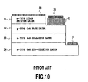
- FIG. 10 is a schematic view showing a conventional HBT structure that has a p-type GaN regrown on the p-type GaN base layer that suffers the etching damage, that is, a schematic view showing a conventional HBT structure that has a new p-type semiconductor grown on the p-type nitride semiconductor base layer.
- the HBT structure has an n-type GaN sub-collector layer 34, an n-type GaN collector layer 33 stacked on the n-type GaN sub-collector layer 34, a p-type GaN base layer 32 stacked on the n-type GaN collector layer, an n-type AlGaN emitter layer 31 stacked on the p-type GaN base layer 32, and an external regrown p-type GaN base layer 35 formed on the p-type GaN base layer 32 whose surface is exposed.
- the HBT structure has a collector electrode 37 formed on the n-type GaN sub-collector layer 34 whose surface is exposed, a base electrode 36 formed on the external regrown p-type GaN base layer 35, and an emitter electrode 38 formed on the n-type AlGaN emitter layer 31.
- the offset voltage in the common emitter I-V characteristics is equal to or larger than 4 V. Furthermore, as for the foregoing non-patent document 4, the offset voltage cannot be determined because the common emitter I-V characteristics reported have a large leakage current.
- the regrowth of the p-type GaN (sometimes referred to as an "external base layer") on the base layer exposed by etching can little improve the HBT characteristics.
- the regrowth using the p-type GaN is considered to be unable to improve the HBT characteristics because the process damage at the regrowth interface cannot be recovered. This teaches that a material to be regrown is important to fabricate good HBTs.
- a second method regrows a p-type GaAs on the surface that suffers the damage instead of regrowing the p-type GaN (for example, refer to a non-patent document 5, K. P. Lee, A. P. Zhang, G. Dang, F. Ren, J. Han, S. N. G. Chu, W. S. Hobson, J. Lopata, C. R. Abernathy, S. J. Pearton, and J. W. Lee, Solid-State Electronics 45, pp. 243-247 (2001 )).
- the hole concentration of the p-type GaAs is 10 20 cm -3 , which is 100 times or more higher than the hole concentration of the p-type GaN in the room temperature.
- the document 5 is a report that pays attention to such a high hole concentration to achieve the good HBT characteristics.
- the regrowth of the p-type GaAs cannot achieve the current gain larger than 5 and the offset voltage less than 3.5 V in the common emitter I-V characteristics, thereby being unable to achieve the good HBT characteristics.
- the HBT characteristics are considered to be unimproved because the process damage between the p-type GaN base layer and the p-type GaAs grown layer has not been repaired. This teaches that a good HBT cannot be fabricated by only increasing the hole concentration of the layer regrown on the p-type GaN that suffers the process damage.
- Japanese patent application laid-open Nos. 5-175225 (1993 ) and 5-291282 (1993 ) are known.
- the documents disclose a technique that regrows a p-type GaAs external base layer on an AlGaAs external emitter layer whose resistance is increased, to reduce the junction capacitance.
- Japanese patent application laid-open No. 7-245316 (1995 ) discloses a device that has a p-type GaAs external base layer on an n-type GaAs collector layer via an n-type InGaP etching stopper layer.
- the present invention is implemented to solve the foregoing problems. Therefore it is an object of the present invention to provide a p-type nitride semiconductor structure capable of forming a good ohmic electrode by solving a problem in that it is difficult to form the good ohmic electrode on the surface of the p-type nitride semiconductor processed.
- Another object of the present invention is to provide a p-type nitride semiconductor bipolar transistor having a greatly improved current gain by solving a problem in that the conventional p-type nitride semiconductor bipolar transistors have a current gain much smaller than the current gain of the bipolar transistors fabricated from other semiconductors.
- Still another object of the present invention is to provide a p-type nitride semiconductor bipolar transistor capable of reducing the offset voltage to a value close to the value expected from the band gaps of emitter and base materials by solving a problem in that the conventional p-type nitride semiconductor bipolar transistor has a offset voltage much larger than the value expected from the band gaps.
- a characteristic of the present invention is that it has a structure in which the indium-containing p-type nitride semiconductor is regrown on the p-type nitride semiconductor processed. It differs from the conventional technique in that the regrown p-type nitride semiconductor contains In.
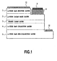
- FIG. 1 is a schematic view showing an HBT structure in accordance with the present invention, a structural view of a p-type nitride semiconductor bipolar transistor.
- the HBT structure has an n-type GaN sub-collector layer 5, an n-type GaN collector layer 4 stacked on the n-type GaN sub-collector layer 5, a graded InGaN layer 3 stacked on the n-type GaN collector layer 4, a p-type InGaN base layer 2 stacked on the graded InGaN layer 3, an n-type GaN emitter layer 1 stacked on the p-type InGaN base layer 2, and an external regrown p-type InGaN base layer 8 formed on the p-type InGaN base layer 2 whose surface is exposed.
- the HBT structure has a collector electrode 10 formed on the n-type GaN sub-collector layer 5 whose surface is exposed, a base electrode 9 formed on the external regrown p-type InGaN base layer 8, and an emitter electrode 11 formed on the n-type GaN emitter layer 1.
- the HBT which is a p-type nitride semiconductor HBT having the base layer 2 composed of a p-type nitride semiconductor, has the p-type nitride semiconductor layer 8 that contains In and is grown on the surface of the p-type base layer 2 which is exposed by etching the emitter layer 1.
- the p-type base layer 2 in accordance with the present invention is p-type InGaN containing In.
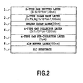
- FIG. 2 is a schematic view showing a grown layer structure.
- the emitter layer 1 is composed of n-type GaN (Si: 5 ⁇ 10 19 cm -3 , 40 nm);
- the base layer 2 is composed of p-type InGaN (In: 7%, Mg: 1 ⁇ 10 19 cm -3 , 100 nm);
- the graded layer 3 is composed of InGaN (30 nm);
- the collector layer 4 is composed of n-type GaN (Si: 1 ⁇ 10 17 cm -3 , 500 nm);
- the sub-collector layer 5 is composed of n-type GaN (1 ⁇ m);
- the buffer layer 6 is composed of A1N (100 nm); and
- the substrate 7 is composed of SiC.
- the collector layer 4 was grown at 1000 °C using trimethylgallium and ammonia.
- the graded InGaN layer 3, base layer 2, and emitter layer 1 were grown at 780 °C using trimethylindium, triethyl gallium and ammonia.
- Mg atoms were used as the p-type impurity, and Si atoms were used as the n-type impurity.
- the In mole fraction in the InGaN was measured using X-ray diffraction measurements XRD) by applying Vegard's law under the assumption that the InGaN crystals were completely relaxed.
- the present embodiment sets the In mole fraction of the p-type InGaN at a rather small value of about 7%.
- a small In mole fraction will increase the effect of the process damage (see, non-patent document 1, for example). Accordingly, it is considered that there is a tradeoff between the current gain and process damage.
- the In mole fraction of the p-type InGaN base layer 2 is preferably from 5% to 30%, and the In mole fraction of the p-type nitride semiconductor layer 8 is higher than that of the p-type InGaN base layer 2.
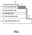
- the HBT layer structure as shown in FIG. 2 was processed by dry etching (reactive ion etching) using chlorine-containing gases to expose the surface of the base layer 2 and that of the sub-collector layer 5.
- the p-type InGaN external base layer 8 was regrown on the p-type InGaN base layer 2 using trimethylindium, triethylgallium, cyclopentadienyl magnesium (source gas of Mg atoms) and ammonia. Since it is preferable that the growth temperature of the regrowth be lower than the growth temperature of the base layer 2 (which is 780 °C in the present embodiment), it is set at 750 °C in the present embodiment.
- the In mole fraction of the p-type InGaN external base layer 8 to be regrown is preferably higher than the In mole fraction of the p-type InGaN layer 2.
- FIG. 3 is a schematic view showing a state after the regrowth. Afterward, the SiO 2 mask 12 was removed with HF, followed by forming the individual electrodes (base electrode 9, collector electrode 10 and emitter electrode 11) by electron beam evaporation. In this way, the HBT as shown in FIG. 1 was finally fabricated. In this case, the size of the emitter electrode 11 is 50 ⁇ m ⁇ 30 ⁇ m.
- FIG. 4 shows a detailed structure of the p-type InGaN external base layer 8 regrown in the present embodiment.
- a 100 nm thick p-type InGaN layer 17 with the In mole fraction of 20% was regrown, followed by growing a thin p-type InGaN layer 13 with a thickness of 2 nm and the In mole fraction of 30%.
- the Mg concentration contained in the regrown p-type InGaN layers is 4 ⁇ 10 19 cm -3 .
- polarization charge 14 occurs because of the distortion of crystals.
- the nitride semiconductor is characterized by having large polarization charge.
- GaAs-based or InP-based compound semiconductors have only negligible polarization charge.
- negative polarization charge takes place at the interface. Utilizing the property makes it possible to reduce the contact resistance between the p-type nitride semiconductor and a metal (see, Japanese patent application laid-open No.
- the thin p-type InGaN layer 13 plays a role of only reducing the contact resistance with a metal, and the foregoing documents do not disclose the substance of the present invention.
- the regrowth of the p-type InGaN layer 17 with the thickness of 100 nm and the In mole fraction of 20% on the p-type InGaN base layer 2 is the subject matter of the present invention.
- the p-type InGaN external base layer 17 with the In mole fraction of 20% have the Mg concentration higher than the p-type InGaN base layer 2 with the In mole fraction of 7%.
- the Mg concentration it is preferable that the Mg concentration be from 1 ⁇ 10 19 cm -3 to 2 ⁇ 10 20 cm -3 .
- its thickness is preferably from 1 nm to 1000 nm.
- defects due to etching bring about positive charges 16 on the p-type InGaN base layer 2.
- the positive charges 16 cause the deterioration in the ohmic characteristics.
- the p-type InGaN external base layer 17 whose In mole fraction is 20% is not distorted completely, a certain degree of negative polarization charges 15 are expected to occur between the layer 17 and the p-type InGaN base layer 2 whose In mole fraction is 7%.
- the negative charges 15 are expected to improve the ohmic characteristics by canceling out the positive charges 16 due to the defects. Accordingly, it is preferable the regrown p-type InGaN external base layer 17 has an In mole fraction higher than that of the p-type InGaN base layer 2.
- Two Pd/Au electrodes 9 were formed on the p-type InGaN external base layer 8 which was regrown in the present embodiment, and the I-V characteristics across the two electrodes were measured.
- the size of the electrodes is 50 ⁇ m ⁇ 80 ⁇ m, and their distance is 20 ⁇ m.
- the regrown base layer 8 is not regrown in regions where the electrodes are not formed. Thus, all the current passes through the interface between the p-type InGaN base layer 2 whose In mole factor is 7% and the regrown p-type InGaN external base layer 17 whose In mole factor is 20%.
- FIG. 5 is a comparative graph illustrating the I-V characteristics when the p-type InGaN external base layer 8 is regrown (embodiment) and the I-V characteristics when it is not regrown (conventional method).
- the conventional method cannot achieve good ohmic characteristics because of the etching damage.
- the I-V characteristics are greatly improved in the present embodiment that regrows the p-type InGaN external base layer 8.
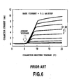
- FIG. 5 illustrates an example of the common emitter I-V characteristics introduced in the non-patent document 2.
- the HBT which employs the p-type InGaN layer as the base layer, has lesser process damage than the HBT using the p-type GaN. Nevertheless, the maximum value of the current gain is about 20, and the offset voltage is about 6 V. The deviation of the offset voltage from the expected value is not less than 5 V.
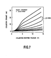
- the HBT common emitter I-V characteristics of the present embodiment is illustrated in FIG. 7 .
- the maximum value of the current gain is equal to or greater than 3000.
- FIG. 8 illustrates the common emitter I-V characteristics measured at small currents to check the offset voltage.
- the offset voltage is 0.27 V.
- the conduction band discontinuity between the n-type GaN emitter layer 1 and the p-type InGaN base layer 2 whose In mole fraction is 7% is 0.2 V.
- the offset voltage nearly equal to the discontinuity can be achieved.
- the deviation of the offset voltage from the expected value is not more than 0.1 V. In this way, compared with the HBT fabricated by the conventional method, the HBT of the present embodiment can sharply increase the current gain by a factor of 100 and more, and greatly reduce the deviation of the offset voltage from the expected value to less than 1/50.
- the process damage is restored by regrowing the indium-containing p-type nitride semiconductor on the p-type nitride semiconductor having the process damage. This can greatly improve the ohmic characteristics. As a result, applying the present invention to the HBT base layer offers an advantage of being able to greatly improve the current gain and the offset voltage.
Landscapes
- Bipolar Transistors (AREA)
Abstract
Description
- The present invention relates to a p-type nitride semiconductor structure and bipolar transistor, and more particularly to a p-type nitride semiconductor structure having nitride semiconductors, and a p-type nitride semiconductor bipolar transistor used for high-output power amplifiers and the like.
- Prior art which is related to this field of technology can be found e.g. in document MAKIMOTO TOSHIKI ET AL: "High current gains obtained by InGaN/GaN double heterojunction bipolar transistors with p-InGaN base", APPLIED PHYSICS LETTERS, AIP, AMERICAN INSTITUTE OF PHYSICS, MELVILLE, NY, vol. 79, no. 3, 16 July 2001 (2001-07-16), pages 380-381, document KUMAKURA K. ET AL: "Low-resistance nonalloyed ohmic contact to p-type GaN using strained InGaN contact layer", APPLIED PHYSICS LETTERS, vol. 79, no. 16, 15 October 2001, pages 2588 - 2590, document
JP 2002-305204 A JP 10-065216 A US 2002/0146855 A1 disclosing a nitride-based semiconductor laser device and method of forming the same. - Generally, nitride semiconductors are widely used for various optoelectronic devices because of their characteristics of having a wide band gap. Surfaces of p-type nitride semiconductors processed by etching or the like suffer damage because of the processing. Since the damage exhibits n-type conductivity, the processed p-type nitride semiconductors cannot achieve good ohmic current-voltage (I-V) characteristics even if ohmic electrodes are formed on the surfaces of the p-type nitride semiconductors (for example, refer to non-patent document 1, T. Makimoto, K. Kumakura, and N. Kobayashi, Journal of Crystal Growth 221, pp. 350-355, (2000); non-patent
document 2, T. Makimoto, K. Kumakura, and N. Kobayashi, phys. stat. sol.(a) 188, No. 1, pp. 183-186, (2001)). - To reduce the effect of the damage, a method is reported of growing a new p-type semiconductor on the layer that suffers the damage. Here, studies concerning an npn-type nitride semiconductor heterojunction bipolar transistor (HBT) having a base layer consisting of a p-type nitride semiconductor will be mainly described.
-
FIGs. 9A-9E are views showing a typical process of fabricating an HBT:FIG. 9A shows crystal growth of the HBT structure;FIG. 9B shows surface exposure of the base layer by etching;FIG. 9C shows surface exposure of the sub-collector layer by etching;FIG. 9D shows forming of a p-type electrode on the base layer; andFIG. 9E shows forming of n-type electrodes on the emitter layer and sub-collector layer. - As shown
FIG. 9A , the HBT structure has an n-type sub-collector layer 24, an n-type collector layer 23 stacked on the n-type sub-collector layer 24, a p-typeInGaN base layer 22 stacked on the n-type collector layer 23, and an n-typeGaN emitter layer 21 stacked on the p-typeInGaN base layer 22. Subsequently, as shown inFIG. 9B , the surface exposure of thebase layer 22 is carried out by etching. Then, as shown inFIG. 9C , the surface exposure of the n-type sub-collector layer 24 is carried out by etching. Subsequently, as shown inFIG. 9D , a p-type electrode (base electrode) 25 is formed on thebase layer 22 whose surface is exposed. Finally, as shown inFIG. 9E , n-type electrodes 26 are formed on theemitter layer 21 and the n-type sub-collector layer 24 whose surface is exposed. - In the HBT fabrication process, the surface of the
base layer 22 is exposed by removing theemitter layer 21 by etching to form thebase electrode 25. Thebase electrode 25 is formed on the surface of the exposedbase layer 22. Since the surface of the exposedbase layer 22 suffers the etching damage, the base electrode does not exhibit good ohmic I-V characteristics, when thebase layer 22 is p-type GaN. As a result, the fabricated HBT does not exhibit good common emitter I-V characteristics. - In other words, the conventional nitride HBT has the common emitter I-V characteristics that present a problem of having a small current gain and a high offset voltage. To reduce the effect of the damage of the surface of the base layer, several methods are reported of growing a new p-type semiconductor on the p-type nitride semiconductor base layer that suffers the damage.
- The conventional methods will be described.
- A first method of reducing the effect of the damage is that of regrowing a p-type GaN on the surface that suffers the damage (for example, see, non-patent document 3, L. S. McCarthy, P. Kozodoy, M. J. W. Rodwell, S. P. DenBaars, and U. K. Mishra, IEEE Electron Device Letters, Vol. 20, No. 6, pp. 277-279 (1999); or non-patent document 4, B. S. Shelton, D. J. H. Lambert, Jian Jang Huang, M. M. Wong, U. Chowdhury, Ting Gang Zhu, H. K. Kwon, Z. Liliental-Weber, M. Benarama, M. Feng, and R. D. Dupuis, IEEE Transactions on Electron Devices, Vol. 48, No. 3, pp. 490-494 (2001)).
-
FIG. 10 is a schematic view showing a conventional HBT structure that has a p-type GaN regrown on the p-type GaN base layer that suffers the etching damage, that is, a schematic view showing a conventional HBT structure that has a new p-type semiconductor grown on the p-type nitride semiconductor base layer. The HBT structure has an n-typeGaN sub-collector layer 34, an n-typeGaN collector layer 33 stacked on the n-typeGaN sub-collector layer 34, a p-typeGaN base layer 32 stacked on the n-type GaN collector layer, an n-typeAlGaN emitter layer 31 stacked on the p-typeGaN base layer 32, and an external regrown p-typeGaN base layer 35 formed on the p-typeGaN base layer 32 whose surface is exposed. In addition, the HBT structure has acollector electrode 37 formed on the n-typeGaN sub-collector layer 34 whose surface is exposed, abase electrode 36 formed on the external regrown p-typeGaN base layer 35, and anemitter electrode 38 formed on the n-typeAlGaN emitter layer 31. - In spite of the regrowth of the base layer, however, none of the methods disclosed in the foregoing non-patent documents can achieve the HBT current gain larger than 10, which shows that a large gain cannot be achieved.
- In addition, in the foregoing non-patent document 3, the offset voltage in the common emitter I-V characteristics is equal to or larger than 4 V. Furthermore, as for the foregoing non-patent document 4, the offset voltage cannot be determined because the common emitter I-V characteristics reported have a large leakage current.
- As described above, the regrowth of the p-type GaN (sometimes referred to as an "external base layer") on the base layer exposed by etching can little improve the HBT characteristics. The regrowth using the p-type GaN, a typical example of the p-type nitride semiconductors, is considered to be unable to improve the HBT characteristics because the process damage at the regrowth interface cannot be recovered. This teaches that a material to be regrown is important to fabricate good HBTs.
- A second method regrows a p-type GaAs on the surface that suffers the damage instead of regrowing the p-type GaN (for example, refer to a
non-patent document 5, K. P. Lee, A. P. Zhang, G. Dang, F. Ren, J. Han, S. N. G. Chu, W. S. Hobson, J. Lopata, C. R. Abernathy, S. J. Pearton, and J. W. Lee, Solid-State Electronics 45, pp. 243-247 (2001)). The hole concentration of the p-type GaAs is 1020 cm-3, which is 100 times or more higher than the hole concentration of the p-type GaN in the room temperature. Thedocument 5 is a report that pays attention to such a high hole concentration to achieve the good HBT characteristics. - The regrowth of the p-type GaAs, however, cannot achieve the current gain larger than 5 and the offset voltage less than 3.5 V in the common emitter I-V characteristics, thereby being unable to achieve the good HBT characteristics. In this case also, the HBT characteristics are considered to be unimproved because the process damage between the p-type GaN base layer and the p-type GaAs grown layer has not been repaired. This teaches that a good HBT cannot be fabricated by only increasing the hole concentration of the layer regrown on the p-type GaN that suffers the process damage.
- As relevant patent documents, Japanese patent application laid-open Nos.
5-175225 (1993 5-291282 (1993 7-245316 (1995 - The present invention is implemented to solve the foregoing problems. Therefore it is an object of the present invention to provide a p-type nitride semiconductor structure capable of forming a good ohmic electrode by solving a problem in that it is difficult to form the good ohmic electrode on the surface of the p-type nitride semiconductor processed.
- Another object of the present invention is to provide a p-type nitride semiconductor bipolar transistor having a greatly improved current gain by solving a problem in that the conventional p-type nitride semiconductor bipolar transistors have a current gain much smaller than the current gain of the bipolar transistors fabricated from other semiconductors.
- Still another object of the present invention is to provide a p-type nitride semiconductor bipolar transistor capable of reducing the offset voltage to a value close to the value expected from the band gaps of emitter and base materials by solving a problem in that the conventional p-type nitride semiconductor bipolar transistor has a offset voltage much larger than the value expected from the band gaps.
- The above is accomplished according to what is set forth in the appended independent claim. Advantageous modifications are set forth the in the appended dependent claims.
- A characteristic of the present invention is that it has a structure in which the indium-containing p-type nitride semiconductor is regrown on the p-type nitride semiconductor processed. It differs from the conventional technique in that the regrown p-type nitride semiconductor contains In.
- Growing the indium-containing p-type nitride semiconductor on the p-type nitride semiconductor that suffers the process damage makes it possible to achieve a good regrowth interface because of the In atoms, thereby being able to greatly reduce the process damage. As a result, good ohmic electrodes can be formed. Applying the present invention to the regrowth of the external p-type base layer of the bipolar transistor can reduce the base leakage current caused by the process damage. As a result, it can achieve the marked improvement of the current gain and the low offset voltage.
-
FIG. 1 is a schematic view showing an HBT structure in accordance with the present invention; -
FIG. 2 is a schematic view showing a layer structure of an npn-type HBT used by an embodiment; -
FIG. 3 is a schematic view showing a state after the regrowth of a p-type InGaN external base layer; -
FIG. 4 is a diagram showing details near the regrown p-type InGaN external base layer in the embodiment; -
FIG. 5 is a comparative graph illustrating I-V characteristics in the case where the p-type InGaN is regrown (the present invention), and the I-V characteristics in the case where it is not regrown (conventional structure); -
FIG. 6 is a graph illustrating an example of the common emitter I-V characteristics of an HBT fabricated by a conventional method; -
FIG. 7 is a graph illustrating an example of the common emitter I-V characteristics of an HBT of the embodiment; -
FIG. 8 is a graph illustrating an example of the common emitter I-V characteristics measured using a small current to check a offset voltage; -
FIGs. 9A-9E are views showing an example of a typical conventional process (without the regrowth) of fabricating an HBT; and -
FIG. 10 is a schematic view showing a conventional HBT structure in the case where p-type GaN is regrown on p-type GaN that suffers etching damage. - A preferred embodiment of the present invention will now be described with reference to the accompanying drawings.
-
FIG. 1 is a schematic view showing an HBT structure in accordance with the present invention, a structural view of a p-type nitride semiconductor bipolar transistor. - The HBT structure has an n-type
GaN sub-collector layer 5, an n-type GaN collector layer 4 stacked on the n-typeGaN sub-collector layer 5, a graded InGaN layer 3 stacked on the n-type GaN collector layer 4, a p-typeInGaN base layer 2 stacked on the graded InGaN layer 3, an n-type GaN emitter layer 1 stacked on the p-typeInGaN base layer 2, and an external regrown p-type InGaN base layer 8 formed on the p-typeInGaN base layer 2 whose surface is exposed. In addition, the HBT structure has acollector electrode 10 formed on the n-typeGaN sub-collector layer 5 whose surface is exposed, abase electrode 9 formed on the external regrown p-type InGaN base layer 8, and anemitter electrode 11 formed on the n-type GaN emitter layer 1. - The HBT, which is a p-type nitride semiconductor HBT having the
base layer 2 composed of a p-type nitride semiconductor, has the p-type nitride semiconductor layer 8 that contains In and is grown on the surface of the p-type base layer 2 which is exposed by etching the emitter layer 1. The p-type base layer 2 in accordance with the present invention is p-type InGaN containing In. - A fabrication method of the HBT in accordance with the present invention will now be described.
- First, an npn-type HBT is fabricated on a SiC substrate 7 using metalorganic vapor phase epitaxy (MOVPE).
FIG. 2 is a schematic view showing a grown layer structure. The emitter layer 1 is composed of n-type GaN (Si: 5 × 1019 cm-3, 40 nm); thebase layer 2 is composed of p-type InGaN (In: 7%, Mg: 1 × 1019 cm-3, 100 nm); the graded layer 3 is composed of InGaN (30 nm); the collector layer 4 is composed of n-type GaN (Si: 1 × 1017 cm-3, 500 nm); thesub-collector layer 5 is composed of n-type GaN (1 µm); thebuffer layer 6 is composed of A1N (100 nm); and the substrate 7 is composed of SiC. The collector layer 4 was grown at 1000 °C using trimethylgallium and ammonia. The graded InGaN layer 3,base layer 2, and emitter layer 1 were grown at 780 °C using trimethylindium, triethyl gallium and ammonia. Mg atoms were used as the p-type impurity, and Si atoms were used as the n-type impurity. The In mole fraction in the InGaN was measured using X-ray diffraction measurements XRD) by applying Vegard's law under the assumption that the InGaN crystals were completely relaxed. - When the In mole fraction in the p-type InGaN which constitutes the
base layer 2 increases, the lattice constant difference between the p-type InGaN and GaN increases, and hence the defect density increases. As a result, the life time of the minority carrier is shortened, which will reduce the current gain. Thus, the present embodiment sets the In mole fraction of the p-type InGaN at a rather small value of about 7%. In contrast with this, a small In mole fraction will increase the effect of the process damage (see, non-patent document 1, for example). Accordingly, it is considered that there is a tradeoff between the current gain and process damage. In view of this, the In mole fraction of the p-typeInGaN base layer 2 is preferably from 5% to 30%, and the In mole fraction of the p-type nitride semiconductor layer 8 is higher than that of the p-typeInGaN base layer 2. - In addition, if the p-type
InGaN base layer 2 is simply joined to the n-type GaN collector layer 4, potential spikes will occur between thebase layer 2 and collector layer 4 because of the conduction band discontinuity. The potential spikes will reduce the current gain because they hinder the electrons injected from the emitter layer 1 to thebase layer 2 from moving toward the collector layer 4. To eliminate such effect, the graded InGaN layer 3 whose In mole fraction is gradually varied is inserted between thebase layer 2 and collector layer 4. - First, the HBT layer structure as shown in
FIG. 2 was processed by dry etching (reactive ion etching) using chlorine-containing gases to expose the surface of thebase layer 2 and that of thesub-collector layer 5. - Subsequently, regions at which the regrowth of the p-type nitride semiconductor layer 8 is to be avoided are covered with a SiO2 mask. Then, the p-type InGaN external base layer 8 was regrown on the p-type
InGaN base layer 2 using trimethylindium, triethylgallium, cyclopentadienyl magnesium (source gas of Mg atoms) and ammonia. Since it is preferable that the growth temperature of the regrowth be lower than the growth temperature of the base layer 2 (which is 780 °C in the present embodiment), it is set at 750 °C in the present embodiment. - The In mole fraction of the p-type InGaN external base layer 8 to be regrown is preferably higher than the In mole fraction of the p-
type InGaN layer 2.FIG. 3 is a schematic view showing a state after the regrowth. Afterward, the SiO2 mask 12 was removed with HF, followed by forming the individual electrodes (base electrode 9,collector electrode 10 and emitter electrode 11) by electron beam evaporation. In this way, the HBT as shown inFIG. 1 was finally fabricated. In this case, the size of theemitter electrode 11 is 50 µm × 30 µm. -
FIG. 4 shows a detailed structure of the p-type InGaN external base layer 8 regrown in the present embodiment. On the p-typeInGaN base layer 2 exposed by etching, a 100 nm thick p-type InGaN layer 17 with the In mole fraction of 20% was regrown, followed by growing a thin p-type InGaN layer 13 with a thickness of 2 nm and the In mole fraction of 30%. The Mg concentration contained in the regrown p-type InGaN layers is 4 × 1019 cm-3. In the present example, between the thin p-type InGaN layer 13 whose In mole fraction is 30% and the p-type InGaN layer 17 whose Inmole fraction 20%,polarization charge 14 occurs because of the distortion of crystals. The nitride semiconductor is characterized by having large polarization charge. In contrast, GaAs-based or InP-based compound semiconductors have only negligible polarization charge. When the InGaN with a higher In mole fraction is grown on the InGaN with a lower In mole fraction, negative polarization charge takes place at the interface. Utilizing the property makes it possible to reduce the contact resistance between the p-type nitride semiconductor and a metal (see, Japanese patent application laid-open No.2003-007998 - In other word, the thin p-
type InGaN layer 13 plays a role of only reducing the contact resistance with a metal, and the foregoing documents do not disclose the substance of the present invention. In contrast with this, it should be noted that the regrowth of the p-type InGaN layer 17 with the thickness of 100 nm and the In mole fraction of 20% on the p-typeInGaN base layer 2 is the subject matter of the present invention. - It is preferable that the p-type InGaN
external base layer 17 with the In mole fraction of 20% have the Mg concentration higher than the p-typeInGaN base layer 2 with the In mole fraction of 7%. On the other hand, it is known that too high Mg concentration brings about reduction in the hole carrier concentration. In view of this, it is preferable that the Mg concentration be from 1 × 1019 cm-3 to 2 × 1020 cm-3. In addition, if the p-type InGaNexternal base layer 17 with the In mole fraction of 20% is too thin, the effect of the regrowth cannot be expected, and if it is too thick, it will hamper the device fabrication. Accordingly, its thickness is preferably from 1 nm to 1000 nm. - As shown in
FIG. 4 , defects due to etching bring aboutpositive charges 16 on the p-typeInGaN base layer 2. Thepositive charges 16 cause the deterioration in the ohmic characteristics. In the present embodiment, although the p-type InGaNexternal base layer 17 whose In mole fraction is 20% is not distorted completely, a certain degree of negative polarization charges 15 are expected to occur between thelayer 17 and the p-typeInGaN base layer 2 whose In mole fraction is 7%. Thenegative charges 15 are expected to improve the ohmic characteristics by canceling out thepositive charges 16 due to the defects. Accordingly, it is preferable the regrown p-type InGaNexternal base layer 17 has an In mole fraction higher than that of the p-typeInGaN base layer 2. - Two Pd/
Au electrodes 9 were formed on the p-type InGaN external base layer 8 which was regrown in the present embodiment, and the I-V characteristics across the two electrodes were measured. The size of the electrodes is 50 µm × 80 µm, and their distance is 20 µm. The regrown base layer 8 is not regrown in regions where the electrodes are not formed. Thus, all the current passes through the interface between the p-typeInGaN base layer 2 whose In mole factor is 7% and the regrown p-type InGaNexternal base layer 17 whose In mole factor is 20%. -
FIG. 5 is a comparative graph illustrating the I-V characteristics when the p-type InGaN external base layer 8 is regrown (embodiment) and the I-V characteristics when it is not regrown (conventional method). The conventional method cannot achieve good ohmic characteristics because of the etching damage. In contrast with this, it is seen that the I-V characteristics are greatly improved in the present embodiment that regrows the p-type InGaN external base layer 8. - A conventional HBT was fabricated through a typical HBT process of
FIG. 9 without applying the present invention.FIG. 5 illustrates an example of the common emitter I-V characteristics introduced in thenon-patent document 2. The HBT, which employs the p-type InGaN layer as the base layer, has lesser process damage than the HBT using the p-type GaN. Nevertheless, the maximum value of the current gain is about 20, and the offset voltage is about 6 V. The deviation of the offset voltage from the expected value is not less than 5 V. - On the other hand, the HBT common emitter I-V characteristics of the present embodiment is illustrated in
FIG. 7 . The maximum value of the current gain is equal to or greater than 3000.FIG. 8 illustrates the common emitter I-V characteristics measured at small currents to check the offset voltage. As can be seen fromFIG. 8 , the offset voltage is 0.27 V. The conduction band discontinuity between the n-type GaN emitter layer 1 and the p-typeInGaN base layer 2 whose In mole fraction is 7% is 0.2 V. Thus, the offset voltage nearly equal to the discontinuity can be achieved. The deviation of the offset voltage from the expected value is not more than 0.1 V. In this way, compared with the HBT fabricated by the conventional method, the HBT of the present embodiment can sharply increase the current gain by a factor of 100 and more, and greatly reduce the deviation of the offset voltage from the expected value to less than 1/50. - As described above, using the p-type InGaN external base layer 8 as the regrowth layer makes it possible to greatly improve the HBT characteristics. The reason for this is considered that the In atoms contained in the p-type nitride semiconductor repair the process damage.
- As described above, according to the present invention, the process damage is restored by regrowing the indium-containing p-type nitride semiconductor on the p-type nitride semiconductor having the process damage. This can greatly improve the ohmic characteristics. As a result, applying the present invention to the HBT base layer offers an advantage of being able to greatly improve the current gain and the offset voltage.
Claims (5)
- A p-type nitride semiconductor structure comprising on a substrate:an n-type collector layer (4, 5);a p-type base layer (2) formed on said n-type collector layer (4, 5), wherein said p-type base layer (2) is p-type InGaN;an n-type emitter layer (1) formed on a part of a top surface of said p-type base layer (2);an indium-containing p-type nitride semiconductor layer (8) regrown on another part of said top surface, that is exposed by etching said n-type emitter layer (1), where said n-type emitter layer (1) is not formed, of said p-type base layer (2), wherein said indium-containing p-type nitride semiconductor layer (8) has an indium mole fraction higher than an indium mole fraction of said p-type base layer (2), and does not contact said n-type emitter layer (1).
- The p-type nitride semiconductor structure according to claim 1, wherein said indium-containing p-type nitride semiconductor layer (8) is p-type InGaN.
- The p-type nitride semiconductor structure according to claim 1 or 2, wherein said p-type base layer (2) has an indium mole fraction of 5 - 30%.
- A p-type nitride semiconductor bipolar transistor comprising the p-type nitride semiconductor structure according to any one of claims 1 to 3, wherein said n-type emitter layer (1) is formed directly on a part of a top surface of said p-type base layer (2), and said another part of said top surface and the surface of the sub-collector layer (5) has been exposed by dry etching (reactive ion etching) using chlorine-containing gases.
- The p-type nitride semiconductor bipolar transistor according to claim 4, further comprising a graded layer (3) between said p-type base layer (2) and said n-type collector layer (4, 5), said graded layer (3) has its indium mole fraction varied gradually.
Applications Claiming Priority (3)
| Application Number | Priority Date | Filing Date | Title |
|---|---|---|---|
| JP2003000089 | 2003-01-06 | ||
| JP2003000089 | 2003-01-06 | ||
| PCT/JP2004/000014 WO2004061971A1 (en) | 2003-01-06 | 2004-01-06 | P-type nitride semiconductor structure and bipolar transistor |
Publications (3)
| Publication Number | Publication Date |
|---|---|
| EP1583154A1 EP1583154A1 (en) | 2005-10-05 |
| EP1583154A4 EP1583154A4 (en) | 2009-05-06 |
| EP1583154B1 true EP1583154B1 (en) | 2011-12-28 |
Family
ID=32708758
Family Applications (1)
| Application Number | Title | Priority Date | Filing Date |
|---|---|---|---|
| EP04700296A Expired - Lifetime EP1583154B1 (en) | 2003-01-06 | 2004-01-06 | P-type nitride semiconductor structure and bipolar transistor |
Country Status (5)
| Country | Link |
|---|---|
| US (1) | US7804106B2 (en) |
| EP (1) | EP1583154B1 (en) |
| JP (1) | JPWO2004061971A1 (en) |
| CN (1) | CN1698210A (en) |
| WO (1) | WO2004061971A1 (en) |
Families Citing this family (11)
| Publication number | Priority date | Publication date | Assignee | Title |
|---|---|---|---|---|
| CN100555684C (en) * | 2006-08-02 | 2009-10-28 | 中国科学院半导体研究所 | A kind of gallium nitride based LED device for illumination |
| US8716835B2 (en) | 2008-10-21 | 2014-05-06 | Renesas Electronics Corporation | Bipolar transistor |
| CN102246283B (en) | 2008-10-21 | 2014-08-06 | 瑞萨电子株式会社 | Bipolar transistor |
| JP5647986B2 (en) * | 2009-09-22 | 2015-01-07 | ルネサスエレクトロニクス株式会社 | Semiconductor device, field effect transistor, and electronic device |
| JP5526687B2 (en) * | 2009-09-30 | 2014-06-18 | 住友電気工業株式会社 | Heterojunction bipolar transistor and method of manufacturing heterojunction bipolar transistor |
| RU2512742C1 (en) * | 2012-12-06 | 2014-04-10 | Федеральное Государственное Унитарное Предприятие "Научно-Производственное Предприятие "Пульсар" | Bipolar transistor |
| JP6242678B2 (en) * | 2013-12-25 | 2017-12-06 | 住友化学株式会社 | Nitride semiconductor device and manufacturing method thereof |
| US10263125B2 (en) * | 2014-05-16 | 2019-04-16 | Qorvo Us, Inc. | Varactor diode with heterostructure |
| JP7059771B2 (en) * | 2018-04-19 | 2022-04-26 | 日本電信電話株式会社 | Light receiving element |
| WO2023112252A1 (en) * | 2021-12-16 | 2023-06-22 | 日本電信電話株式会社 | Heterojunction bipolar transistor |
| CN115117209A (en) * | 2022-07-01 | 2022-09-27 | 西安电子科技大学广州研究院 | Gallium nitride heterojunction bipolar photonic transistor and preparation method thereof |
Family Cites Families (11)
| Publication number | Priority date | Publication date | Assignee | Title |
|---|---|---|---|---|
| JPH05175225A (en) | 1991-12-20 | 1993-07-13 | Nippon Telegr & Teleph Corp <Ntt> | Method for manufacturing heterojunction bipolar transistor |
| JP3228431B2 (en) | 1992-04-10 | 2001-11-12 | 日本電信電話株式会社 | Method of manufacturing collector-up structure heterojunction bipolar transistor |
| JPH07245316A (en) | 1994-03-07 | 1995-09-19 | Fujitsu Ltd | Heterojunction bipolar transistor and manufacturing method thereof |
| JPH1065216A (en) | 1996-08-22 | 1998-03-06 | Toyoda Gosei Co Ltd | Group III nitride semiconductor device |
| JP3433075B2 (en) | 1997-11-19 | 2003-08-04 | 株式会社東芝 | Method of manufacturing nitride semiconductor device |
| US6392262B1 (en) * | 1999-01-28 | 2002-05-21 | Nec Corporation | Compound semiconductor device having low-resistive ohmic contact electrode and process for producing ohmic electrode |
| SE9901410D0 (en) * | 1999-04-21 | 1999-04-21 | Abb Research Ltd | Abipolar transistor |
| JP4148664B2 (en) * | 2001-02-02 | 2008-09-10 | 三洋電機株式会社 | Nitride-based semiconductor laser device and method for forming the same |
| JP3816347B2 (en) | 2001-04-05 | 2006-08-30 | 日本電信電話株式会社 | Heterojunction bipolar transistor |
| JP3645233B2 (en) * | 2001-06-07 | 2005-05-11 | 日本電信電話株式会社 | Semiconductor element |
| JP2003007998A (en) | 2001-06-22 | 2003-01-10 | Nippon Telegr & Teleph Corp <Ntt> | Low resistance nitride semiconductor and method for manufacturing the same |
-
2004
- 2004-01-06 EP EP04700296A patent/EP1583154B1/en not_active Expired - Lifetime
- 2004-01-06 CN CNA2004800002798A patent/CN1698210A/en active Pending
- 2004-01-06 WO PCT/JP2004/000014 patent/WO2004061971A1/en not_active Ceased
- 2004-01-06 JP JP2005507665A patent/JPWO2004061971A1/en active Pending
- 2004-01-06 US US10/516,380 patent/US7804106B2/en not_active Expired - Lifetime
Also Published As
| Publication number | Publication date |
|---|---|
| EP1583154A4 (en) | 2009-05-06 |
| JPWO2004061971A1 (en) | 2006-05-18 |
| US20050224831A1 (en) | 2005-10-13 |
| WO2004061971A1 (en) | 2004-07-22 |
| CN1698210A (en) | 2005-11-16 |
| US7804106B2 (en) | 2010-09-28 |
| EP1583154A1 (en) | 2005-10-05 |
Similar Documents
| Publication | Publication Date | Title |
|---|---|---|
| US11031399B2 (en) | Semiconductor device and manufacturing method of the same | |
| JP4022708B2 (en) | Semiconductor device | |
| JP3708810B2 (en) | Nitride III-V compound semiconductor device | |
| US20010015437A1 (en) | GaN field-effect transistor, inverter device, and production processes therefor | |
| JP3398044B2 (en) | Field effect transistor | |
| US20070194295A1 (en) | Semiconductor device of Group III nitride semiconductor having oxide protective insulating film formed on part of the active region | |
| JPH06333937A (en) | Bipolar transistor | |
| JP3449116B2 (en) | Semiconductor device | |
| EP1583154B1 (en) | P-type nitride semiconductor structure and bipolar transistor | |
| JP2004006461A (en) | Semiconductor device | |
| JPH11261052A (en) | High mobility transistor | |
| US6919589B2 (en) | HEMT with a graded InGaAlP layer separating ohmic and Schottky contacts | |
| US7622788B2 (en) | GaN heterojunction bipolar transistor with a p-type strained InGaN base layer | |
| JP2539268B2 (en) | Semiconductor device | |
| JP2007059719A (en) | Nitride semiconductor | |
| JP2008016615A (en) | Bipolar transistor | |
| JP6538608B2 (en) | Method of manufacturing heterojunction bipolar transistor | |
| JP4072858B2 (en) | Nitride III-V compound semiconductor device | |
| JP3180734B2 (en) | Method for manufacturing field effect transistor | |
| JP2007207820A (en) | Field effect transistor and manufacturing method thereof | |
| Bolognesi et al. | InAs/AlSb heterostructure field-effect transistors using a Si-doped InAs/AlSb short-period superlattice modulation doping barrier | |
| JP2000174031A (en) | Heterojunction bipolar transistor | |
| JPH02111073A (en) | Insulated gate fet and integrated circuit device thereof | |
| JP2021019089A5 (en) | ||
| JP2980630B2 (en) | Compound semiconductor device |
Legal Events
| Date | Code | Title | Description |
|---|---|---|---|
| PUAI | Public reference made under article 153(3) epc to a published international application that has entered the european phase |
Free format text: ORIGINAL CODE: 0009012 |
|
| 17P | Request for examination filed |
Effective date: 20041123 |
|
| AK | Designated contracting states |
Kind code of ref document: A1 Designated state(s): AT BE BG CH CY CZ DE DK EE ES FI FR GB GR HU IE IT LI LU MC NL PT RO SE SI SK TR |
|
| AX | Request for extension of the european patent |
Extension state: AL LT LV MK |
|
| DAX | Request for extension of the european patent (deleted) | ||
| RBV | Designated contracting states (corrected) |
Designated state(s): DE FR GB |
|
| A4 | Supplementary search report drawn up and despatched |
Effective date: 20090406 |
|
| GRAP | Despatch of communication of intention to grant a patent |
Free format text: ORIGINAL CODE: EPIDOSNIGR1 |
|
| GRAS | Grant fee paid |
Free format text: ORIGINAL CODE: EPIDOSNIGR3 |
|
| GRAA | (expected) grant |
Free format text: ORIGINAL CODE: 0009210 |
|
| AK | Designated contracting states |
Kind code of ref document: B1 Designated state(s): DE FR GB |
|
| REG | Reference to a national code |
Ref country code: GB Ref legal event code: FG4D |
|
| REG | Reference to a national code |
Ref country code: DE Ref legal event code: R096 Ref document number: 602004035854 Country of ref document: DE Effective date: 20120308 |
|
| PLBE | No opposition filed within time limit |
Free format text: ORIGINAL CODE: 0009261 |
|
| STAA | Information on the status of an ep patent application or granted ep patent |
Free format text: STATUS: NO OPPOSITION FILED WITHIN TIME LIMIT |
|
| 26N | No opposition filed |
Effective date: 20121001 |
|
| REG | Reference to a national code |
Ref country code: DE Ref legal event code: R097 Ref document number: 602004035854 Country of ref document: DE Effective date: 20121001 |
|
| REG | Reference to a national code |
Ref country code: FR Ref legal event code: PLFP Year of fee payment: 13 |
|
| REG | Reference to a national code |
Ref country code: FR Ref legal event code: PLFP Year of fee payment: 14 |
|
| REG | Reference to a national code |
Ref country code: FR Ref legal event code: PLFP Year of fee payment: 15 |
|
| PGFP | Annual fee paid to national office [announced via postgrant information from national office to epo] |
Ref country code: FR Payment date: 20230124 Year of fee payment: 20 |
|
| PGFP | Annual fee paid to national office [announced via postgrant information from national office to epo] |
Ref country code: GB Payment date: 20230119 Year of fee payment: 20 Ref country code: DE Payment date: 20230123 Year of fee payment: 20 |
|
| REG | Reference to a national code |
Ref country code: DE Ref legal event code: R071 Ref document number: 602004035854 Country of ref document: DE |
|
| REG | Reference to a national code |
Ref country code: GB Ref legal event code: PE20 Expiry date: 20240105 |
|
| PG25 | Lapsed in a contracting state [announced via postgrant information from national office to epo] |
Ref country code: GB Free format text: LAPSE BECAUSE OF EXPIRATION OF PROTECTION Effective date: 20240105 |