EP1580823A2 - Organische elektrolumineszente Anzeigevorrichtung und Herstellungsverfahren - Google Patents
Organische elektrolumineszente Anzeigevorrichtung und Herstellungsverfahren Download PDFInfo
- Publication number
- EP1580823A2 EP1580823A2 EP05005409A EP05005409A EP1580823A2 EP 1580823 A2 EP1580823 A2 EP 1580823A2 EP 05005409 A EP05005409 A EP 05005409A EP 05005409 A EP05005409 A EP 05005409A EP 1580823 A2 EP1580823 A2 EP 1580823A2
- Authority
- EP
- European Patent Office
- Prior art keywords
- organic
- film formation
- layer
- layers
- luminescent
- Prior art date
- Legal status (The legal status is an assumption and is not a legal conclusion. Google has not performed a legal analysis and makes no representation as to the accuracy of the status listed.)
- Withdrawn
Links
Images


Classifications
-
- H—ELECTRICITY
- H10—SEMICONDUCTOR DEVICES; ELECTRIC SOLID-STATE DEVICES NOT OTHERWISE PROVIDED FOR
- H10K—ORGANIC ELECTRIC SOLID-STATE DEVICES
- H10K59/00—Integrated devices, or assemblies of multiple devices, comprising at least one organic light-emitting element covered by group H10K50/00
- H10K59/30—Devices specially adapted for multicolour light emission
- H10K59/35—Devices specially adapted for multicolour light emission comprising red-green-blue [RGB] subpixels
-
- H—ELECTRICITY
- H10—SEMICONDUCTOR DEVICES; ELECTRIC SOLID-STATE DEVICES NOT OTHERWISE PROVIDED FOR
- H10K—ORGANIC ELECTRIC SOLID-STATE DEVICES
- H10K50/00—Organic light-emitting devices
- H10K50/80—Constructional details
-
- H—ELECTRICITY
- H10—SEMICONDUCTOR DEVICES; ELECTRIC SOLID-STATE DEVICES NOT OTHERWISE PROVIDED FOR
- H10K—ORGANIC ELECTRIC SOLID-STATE DEVICES
- H10K71/00—Manufacture or treatment specially adapted for the organic devices covered by this subclass
- H10K71/10—Deposition of organic active material
- H10K71/16—Deposition of organic active material using physical vapour deposition [PVD], e.g. vacuum deposition or sputtering
- H10K71/166—Deposition of organic active material using physical vapour deposition [PVD], e.g. vacuum deposition or sputtering using selective deposition, e.g. using a mask
-
- H—ELECTRICITY
- H10—SEMICONDUCTOR DEVICES; ELECTRIC SOLID-STATE DEVICES NOT OTHERWISE PROVIDED FOR
- H10K—ORGANIC ELECTRIC SOLID-STATE DEVICES
- H10K59/00—Integrated devices, or assemblies of multiple devices, comprising at least one organic light-emitting element covered by group H10K50/00
- H10K59/10—OLED displays
- H10K59/12—Active-matrix OLED [AMOLED] displays
-
- H—ELECTRICITY
- H10—SEMICONDUCTOR DEVICES; ELECTRIC SOLID-STATE DEVICES NOT OTHERWISE PROVIDED FOR
- H10K—ORGANIC ELECTRIC SOLID-STATE DEVICES
- H10K59/00—Integrated devices, or assemblies of multiple devices, comprising at least one organic light-emitting element covered by group H10K50/00
- H10K59/10—OLED displays
- H10K59/17—Passive-matrix OLED displays
-
- H—ELECTRICITY
- H10—SEMICONDUCTOR DEVICES; ELECTRIC SOLID-STATE DEVICES NOT OTHERWISE PROVIDED FOR
- H10K—ORGANIC ELECTRIC SOLID-STATE DEVICES
- H10K71/00—Manufacture or treatment specially adapted for the organic devices covered by this subclass
Definitions
- This invention relates to an organic EL (Electroluminescence) panel and a method of manufacturing the same.
- An organic EL panel is produced by forming surface emission elements which are organic EL devices (elements) on a substrate, and forming a displaying area by arranging one or more organic EL devices.
- Each organic EL device is mounted on a substrate and comprises a first electrode, an organic layer including one or more layers of organic compound materials containing at least one organic luminescent layer, and a second electrode, thereby forming a structure with the organic layer interposed between a pair of electrodes.
- film formation areas of layers (such as organic layer) essential for organic EL device (s) are formed corresponding to single or a group of luminescent areas (which may be pixels if display is dot matrix display) to be formed on a substrate.
- luminescent areas which may be pixels if display is dot matrix display
- material layers related to light emission colors it is necessary for material layers related to light emission colors to be formed by different materials in different light emission units.
- the above-mentioned organic layer and electrode layers are sometimes required to be formed into multi-layered structures.
- the foregoing film formation mask is employed to form laminated layers in the film formation areas corresponding to luminescent areas.
- Japanese Unexamined Patent Application Publication Hei 2002-367787 discloses an organic EL panel shown in Fig. 1A.
- a substrate 1 there are formed a plurality of first electrodes 2 consisting of a transparent conductive material such as ITO.
- a plurality of insulating films 3 are arranged to cover the exposed portions (between every two adjacent first electrodes 2) of the substrate 1 as well as part of the periphery of each first electrode 2, thereby dividing the substrate into a plurality of small sections and thus forming a plurality of luminescent areas 45R, 45G, and 45B on the first electrodes2.
- a hole injection layer 40 and a hole transporting layer 41 are formed to cover the first electrodes and spaces therebetween, while areas 60R, 60G, and 60B are selected corresponding to different colors, followed by forming in the respective areas luminescent layers 42R, 42G, and 42B, electron transporting layers 43R, 43G, and 43B, and electron injection layers 44R, 44G, and 44B. Finally, second electrodes 50 are formed over these layers.
- the luminescent layers 42R, 42G, and 42B, the electron transporting layers 43R, 43G, and 43B, and the electron injection layers 44R, 44G, and 44B together form the afore-mentioned organic layer in an organic ELpanel, thus constituting film formation areas corresponding to the luminescent areas 45R, 45G, and 45B.
- the luminescent layer, the electron transporting layer, and an electron injection layer are formed using an identical pattern of the same film formation mask, it is preferred that the formed three layers are overlapped one upon another without any overlap deviation.
- the film formation mask and the substrate have to be positioned relatively to each other for forming each film layer, some troubles in positioning operation will occur and thus film formation area in a certain specific layer will suffer a considerable overlap deviation, resulting in a film formation failure.
- a film formation failure can be detected by an eye-inspection using a microscope or through an image processing. If an inspected state is like that shown in Fig. 1B, it is possible to judge that such a state is a film formation failure. However, it is extremely difficult to judge which layer among the laminated layers has been greatly deviated and thus is a defective layer. On the other hand, in a process of manufacturing an organic EL panel, once a film formation failure occurs at a certain step, similar failures will probably occur in later steps. Accordingly, it is extremely important to detect a specific layer in which a film formation failure has occurred, to re-check a film formation process for forming the specific layer, so as to improve the yield of manufacturing process.
- the present invention has been accomplished to solve the above-discussed problem and it is an object of the invention to provide an improved organic EL panel comprising a substrate and organic EL devices (each formed by interposing an organic layer containing an organic luminescent layer between a pair of electrodes) formed on the substrate, and to provide a method of manufacturing the improved organic EL panel, so that when it is judged that film formation areas of a plurality of layers laminated on an identical luminescent area of an organic EL panel involves a film formation failure, it is possible to determine which layer among the laminated layers involves the film formation failure.
- an organic EL panel and its manufacturing method according to the present invention are characterized by at least the following aspects.
- an improved organic EL panel having a substrate and organic EL devices formed on the substrate, each organic EL device including a pair of electrodes, an organic layer interposed between the pair of electrodes, with the organic layer being formed by laminating a plurality of film layers including an organic luminescent layer.
- film formation areas of a plurality of layers which are essential for forming organic EL devices and laminated on identical luminescent areas of the organic EL devices are formed to have overlap deviations which can be used to identify each of the plurality of film layers.
- the method comprises a film formation step in which film formation areas of layers which are essential for forming organic EL devices are formed on luminescent areas of the organic EL devices corresponding to the pattern of a film formation mask having a plurality of openings. Further, in the film formation step, overlap deviations which can be used to identify each of the plurality of film layers, are formed on the film formation areas of several layers laminated on an identical luminescent area.
- FIGs. 2A and 2B are explanatory views showing an organic EL panel formed according to one embodiment of the present invention.
- an organic EL panel obtained in a predetermined film formation process has film formation areas on a plurality of layers a , b , and c laminated on an identical luminescent area s of the organic EL panel. After film formation, it is possible to observe film formation states shown in Figs. 2A and 2B by using a microscope or through an image processing.
- the plurality of layers a , b , and c are all essential elements for forming organic EL devices and serving as unit surface emission elements of the organic EL panel, and can act as various layers forming an organic layer (containing an organic luminescent functional layer) or act as electrode layers.
- the film formation areas a-c are formed in a manner such that they are overlapped by one another and mutually deviated (overlap and overlap deviation) so as to be distinguishable from one another.
- overlap deviation means an "off-set amount.” Namely, as shown in Fig. 2A, the film formation area of layer b deviates e1 from the film formation area of layer a , the film formation area of layer c deviates e2 from the film formation area of layer b and deviates e3 from the film formation area of layer a .
- the present invention is by no means to be limited by such specific example. Actually, the overlap deviations of the layers are allowed to be in different directions, provided that different layers are distinguishable from one another. Further, although the present embodiment illustrated in Fig. 2A shows that three layers a-c are overlapped by one another and mutually deviated, it is also possible to form "overlap deviation" with all layers laminated on the luminescent area s , or with at least two layers selected from these layers, thereby making it possible to distinguish these layers from one another.
- film formation area of each layer to be formed corresponding to the luminescent area s is usually set larger than the luminescent area s by having an extra portion in length and width directions. Therefore, an amount of the above-mentioned overlap deviation can be set by making use of such extra portions. Namely, as shown in Fig. 2A, the length La of the film formation area of the layer a is set longer than the length Ls of the luminescent area s , thereby setting the overlap deviation amounts e1-e3 within the range of such an extra portion.
- the overlap deviations e1-e3 are set larger than estimated overlap deviation amounts caused due to film formation errors, so as to ensure that the overlap deviations e1-e3 set in advance will not become unrecognizable due to film formation errors (such as mask positioning error, mask designing error, and deposition error).
- Fig. 2A shows an appropriate film formation state in which the respective layers a-c can cover the luminescent area s .
- Fig. 2B shows that a certain layer b has deviated from the luminescent area s and film formation at this time can be judged as a film formation failure.
- e1-e3 overlap deviations
- the above-described overlap deviations are formed in the aforementioned lamination order in the same direction, it is possible to effectively recognize the respective layers. Namely, when the film formation areas are to be laminated on the luminescent area s in the order of layers a , b , c , an operation necessary at this time is only to successively form these overlap deviations in their lamination order in the longitudinal direction, as shown in Fig. 2A. Therefore, if layer b is a film formation failure, such layer can be detected by judging in accordance with such overlap deviation order.
- the direction in which these overlap deviations are formed should not be limited to the longitudinal direction (y direction) shown in Fig. 2A. Actually, the above-described overlap deviations can also be arranged in the lateral direction (x direction) or in a rotated direction ⁇ .
- the present embodiment of the present invention can be effectively applied to an example in which the film formation areas are formed by an identical pattern of a single film formation mask.
- the above-described overlap deviations may be formed by intentionally deviating the position of the film formation mask at the time of forming each layer.
- the present invention should not be limited to such a specific example.
- a film formation mask used in the present invention can be in any desired pattern.
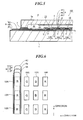
- a film formation mask M 1 having a stripe-like pattern containing linear openings Ma 1 shown in Fig. 3A.
- another film formation mask M 2 having an alternate pattern containing openings Ma 2 corresponding to a group of luminescent areas, as shown in Fig. 3B.
- Figs. 4A and 4B are flow charts briefly showing a method of forming an organic EL panel according to one embodiment of the present invention.
- the method of forming an organic EL panel according to the present invention is almost the same as a conventional method (including pre-processing step S1 ⁇ film formation step S2 ⁇ sealing step S3 ⁇ inspection step S4, as shown in Fig. 4A,), with only the film formation step S2 being different from a conventional one.
- film formation step S2 when film formation areas of layers forming an organic EL device are laminated on the luminescent area s of the organic EL device corresponding to the pattern of a film formation mask, recognizable overlap deviations (for example, overlap deviations e1-e3) are formed on a plurality of layers (for example, layers a-c) to be formed on the identical luminescent area s . Subsequently, a sealing step S3 is performed and an inspection step S4 is thus carried out to perform an eye-inspection or an image-processing on a film formation state of the film formation areas.
- overlap deviations e1-e3 overlap deviations e1-e3
- a sealing step S3 is performed and an inspection step S4 is thus carried out to perform an eye-inspection or an image-processing on a film formation state of the film formation areas.
- film formation is performed by using various materials.
- a film formation mask is set (Sm1) as a first step, and then a first layer of film is formed, followed by repeating the film formation (Smn, Snn). Then, if necessary, other layers of films are formed, thereby finishing the film formation step.
- the setting position of the film formation mask is shifted intentionally, thereby forming the above-described overlap deviations.
- the amounts of the overlap deviations at this time are set such that an amount of overlap deviation of each layer is larger than an estimated overlap deviation possibly caused by an film formation error, while a maximum overlap deviation amount is set in a manner such that each film formation area will not go beyond the luminescent area s (some extra areas or free margins are formed between the luminescent area s and each film formation area of the layers a-c ).
- the method of manufacturing the organic EL panel of the present embodiment of the present invention (as described above) , it is possible to effectively detect a film formation failure during an eye-inspection or an image processing inspection to be performed after the film formation, without having to add some other additional steps as compared with a conventional process except that the film formation mask is set in the manner as described above.
- an organic EL panel having linearly arranged luminescent areas containing three colors of RGB.
- a film formation mask is used which has a stripe-like pattern including a plurality of linear openings, and linear areas of several film layers are formed on the luminescent area by painting different colors on different liner areas.
- Fig. 5 is an explanatory view (a cross sectional view) showing the structure of an organic EL panel 100 formed according to the present embodiment.
- the organic EL panel 100 is formed by interposing an organic layer 4 containing an organic luminescent layer between first electrodes 2 on one hand and second electrodes 5 on the other, thereby forming a plurality of organic EL devices 10 on the substrate 1.
- a silicone coating layer 1a is formed on the substrate 1, and a plurality of first electrodes 2 consisting of transparent electrode material such as ITO and serving as cathodes are formed on the silicon coating layer 1a.
- second electrodes 5 consisting of a metal and serving as anodes are formed above the first electrodes 2, thereby forming a bottom emission type panel producing light from the substrate 1 side.
- the panel also contains an organic layer 4 including a hole transporting layer 4A, a luminescent layer 4B, and an electron transporting layer 4C.
- a cover 6 is bonded to the substrate 1 through an adhesive layer 7, thereby forming a sealing space M on the substrate 1 and thus forming a display section consisting of organic EL devices 10 within the sealing space M.
- the organic EL devices 10 are formed such that the first electrodes 2 are separated by a plurality of insulating strips 3, thereby forming luminescent units (10R, 10G, 10B) under the first electrodes 2. Moreover, a desiccant layer 6A is attached to the inner surface of the cover 6, thereby preventing the organic EL devices 10 from getting deteriorated due to moisture.
- first electrode layer 8A using the same material and the same step as forming the first electrodes 2, which is separated from the first electrodes 2 by the insulating strips 3.
- second electrode layer 8B containing a silver alloy and forming a low-resistant wiring portion.
- a protection coating layer 8C consisting of IZO or the like is formed on the second electrode layer 8C.
- a lead-out electrode 8 can be formed which consists of the first electrode layer 8A, the second electrode layer 8B, and the protection coating 8C. Then, an end portion 5a of each second electrode 5 is connected to the lead-out electrode 8 within the sealing space M.
- each first electrode 2 is not shown in the drawing, it is possible to elongate each first electrode 2 and lead the same out of the sealing space M.
- lead-out electrode can also be formed into an electrode layer containing Ag alloy or the like and constituting a low resistant wiring portion.
- the organic EL panel 100 of the present embodiment since the respective layers (the hole transporting layer 4A, the luminescent layer 4B, and the electron transporting layer 4C) of the organic layer 4 are painted with different colors, it is possible to form film formation areas corresponding to the luminescent units 10R, 10G, and 10B.
- the present embodiment shows an organic layer 4 having a three-layer structure, the present invention should not be limited by three-layer structure.
- a structure including, from the anode side, a hole injection layer (common to RGB)/a first hole transporting layer (common to RGB)/a second hole transporting layer (painted with different colors)/a first organic luminescent layer (painted with different colors)/a second organic luminescent layer (painted with different colors)/a first electron transporting layer (painted with different colors)/a second electron transporting layer (common to RGB)/an electron-injection layer (common to RGB)/(cathode).
- a hole injection layer common to RGB
- a first hole transporting layer common to RGB
- a second hole transporting layer painted with different colors
- a first organic luminescent layer painted with different colors
- a second organic luminescent layer painted with different colors
- a first electron transporting layer painted with different colors
- a second electron transporting layer common to RGB
- an electron-injection layer common to RGB
- four layers including the second hole transporting layer, the first organic luminescent layer, the second organic luminescent layer, and the first electron transporting layer, all painted with different colors, are formed as film formation areas corresponding to the luminescent units 10R, 10G and 10B, on the luminescent units 10R, 10G, and 10B.
- film formation areas of layers laminated on the same luminescent units 10R (10G, 10B), are formed to have overlap deviations for distinguishing one layer from another.
- the respective film formation areas of the hole transporting layer 4A, the luminescent layer 4B, and the electron transporting layer 4C are formed on a linearly arranged area covering a plurality of linearly arranged luminescent units R.
- several overlap deviations e1, e2, and e3 are formed along the longitudinal direction (y direction) of the linear area.
- the film formation mask M 1 having a pattern including a plurality of linear openings M a1 shown in Fig. 3A, whereas the position of the film formation mask M 1 is successively shifted for each layer along the longitudinal direction of the opening M a1 .
- each film formation area when linearly arranging the luminescent units 10R (10G, 10B) of the same color to form a linear film formation area, it is possible to form each film formation area with a relatively large extra portion in the longitudinal direction (y direction) of the luminescent unit 10R (10G, 10B), thereby making it possible to effectively form the above-described overlap deviations e1, e2, and e3 in y direction.
- the present embodiment makes it possible to obtain the same effect as obtainable from the above-described embodiment. Namely, when a film formation failure is judged during an inspection performed after the film formation, it is possible to detect which layer contains such film formation failure by virtue of the overlap deviations e1-e3. In this way, by checking the film formation step which has produced a layer containing the film formation failure and searching out a cause responsible for the film formation failure, it is possible to prevent any similar trouble during subsequent film formation steps.
- Either the first electrodes 2 or the second electrodes 5 are set as cathode side, while the opposite side is set as anode side.
- the anode side is formed by a material having a higher work function than the cathode side, using a transparent conductive film which may be a metal film such as chromium (Cr), molybdenum (Mo), nickel (nickel), and platinum (Pt), or a metal oxide film such as ITO and IZO.
- the cathode side is formed by a material having a lower work function than the anode side, using a metal having a low work function, which may be an alkali metal (such as Li, Na, K, Rb, and Cs), an alkaline earth metal (such as Be, Mg, Ca, Sr, and Ba), a rare earth metal, a compound or an alloy containing two or more of the above elements, or an amorphous semiconductor such as a doped polyaniline and a doped polyphenylene vinylene, or an oxide such as Cr 2 O 3 , NiO, and Mn 2 O 5 .
- a metal having a low work function which may be an alkali metal (such as Li, Na, K, Rb, and Cs), an alkaline earth metal (such as Be, Mg, Ca, Sr, and Ba), a rare earth metal, a compound or an alloy containing two or more of the above elements, or an amorphous semiconductor such as a doped polyaniline and a do
- the lead-out electrodes (the lead-out electrode 8 and the lead-out electrode of the first electrodes 2) are connected with drive circuit parts driving the organic EL panel 100 or connected with a flexible wiring board.
- these lead-out electrodes it is preferable for these lead-out electrodes to be formed as having a low resistance.
- the lead-out electrodes can be formed by laminating low resistant metal electrode layers which may be Ag, Cr, Al, or their alloys, or may be formed by single one electrode of low resistant metal.
- the organic layer 4 comprises one or more layers of organic compound materials including at least one organic luminescent layer
- its laminated structure can be in any desired arrangement.
- a laminated structure including, from the anode side towards the cathode side, a hole transporting layer 4A, a luminescent layer 4B, and an electron transporting layer 4C.
- Each of the hole transporting layer 4A, the luminescent layer 4B, and the electron transporting layer 4C can be in a single-layer or a multi-layered structure.
- the hole transporting layer 4A, the luminescent layer 4B, and the electron transporting layer 4C can be formed by any conventional materials (it is allowed to use either a high molecular material or a low molecular material).
- a luminescent material for forming the luminescent layer 4B it is allowed to make use of a luminescence (fluorescence) when the material returns from a singlet excited state to a base state or a luminescence (phosphorescence) when it returns from a triplet excited state to a base state through a singlet base state.
- a luminescence fluorescence
- phosphorescence luminescence
- the organic EL panel according to the present invention is a panel formed by tightly covering organic EL devices 10 with a covering member 6 made of metal, glass, or plastic.
- the covering member may be a piece of material having a recess portion (a one-step recess or a two-step recess) formed by pressing, etching, or blasting.
- the covering member may be formed by using a flat glass plate and includes an internal covering space M to be formed between the flat glass plate and the support substrate by virtue of a spacer made of glass (or plastic).
- the internal covering space may either be an air-tight space or can be filled with a filler such as a high molecular elastomer, resin or silicon oil.
- an inorganic material may be a nitride such as SiN, AlN, and GaN, or an oxide such as SiO, Al 2 O 3 , Ta 2 O 5 , ZnO, and GeO, or an oxidized nitride such as SiON, or a carbonized nitride such as SiCN, or a metal fluorine compound, or a metal film, etc.
- an organic material may be an epoxy resin, or an acryl resin, or a paraxylene resin, or a fluorine system high molecule such as perfluoro olefin andperfluoro ether, or a metal alkoxide such as CH 3 OM and C 2 H 5 OM, or a polyimide precursor, or a perylene system compound, etc.
- a fluorine system high molecule such as perfluoro olefin andperfluoro ether
- a metal alkoxide such as CH 3 OM and C 2 H 5 OM
- a polyimide precursor such as a perylene system compound, etc.
- An adhesive agent forming the adhesive layer 7 may be a thermal-setting type, a chemical-setting type (2-liquid mixture), or a light (ultraviolet) setting type, which can be formed by an acryl resin, an epoxy resin, a polyester, a polyolefine. Particularly, it is preferable to use an ultraviolet-setting epoxy resin adhesive agent which is quick to solidify without a heating treatment.
- Desiccating material 6A may be a physical desiccating agent such as zeolite, silica gel, carbon, and carbon nanotube; a chemical desiccating agent such as alkali metal oxide, metal halogenide, peroxide chlorine; a desiccating-agent formed by dissolving an organic metallic complex in a petroleum system solvent such as toluene, xylene, an aliphatic organic solvent and the like; and a desiccating agent formed by dispersing desiccating particles in a transparent binder such as polyethylene, polyisoprene, polyvinyl thinnate.
- a physical desiccating agent such as zeolite, silica gel, carbon, and carbon nanotube
- a chemical desiccating agent such as alkali metal oxide, metal halogenide, peroxide chlorine
- a desiccating-agent formed by dissolving an organic metallic complex in a petroleum system solvent such as toluene, xylene, an aliphatic
- the organic EL panel 100 of the present invention can have various types without departing from the scope of the invention.
- the organic EL panel 100 can have a passive drive type based on an electrode arrangement shown in Fig. 5, as well as an active drive type capable of TFT driving each organic EL device 10 acting as a luminescent unit.
- the light emission type of an organic EL device 10 can be a bottom emission type emitting light from the substrate 1 side, or a top emission type emitting light from a side opposite to the substrate 1.
- the EL display panel may be a single color display or a multi-color display.
- CF method, CCM method color conversion layer formed by a color filter or a fluorescent material
- SOLED transparent Stacked OLED
- a thin film of ITO or the like is formed on a glass-substrate 1 through vapor deposition, sputtering or the like, and formed into a desired pattern though photolithography or the like, thereby forming a plurality of first electrodes 2. Further, patterning is performed to form insulating films 3 and allow the openings of the luminescent units 10R, 10G, 10B to be connected with the first electrodes 2 (pre-processing step S1).
- an organic layer 4 is formed by a wet process such as spin coating, dipping, screen printing, ink jet printing and the like, or a dry process such as vapor-deposition, Laser-Induced-Thermal-Imaging (LITI) and the like.
- a hole transporting layer 4A, a luminescent layer 4B, and an electron transporting layer 4C are successively laminated on the luminescent units 10R, 10G, 10B through vapor deposition.
- a coating method utilizing a film-formation mask is used to coat film layers with different colors.
- materials presenting light emissions of three colors RGB or a composite material consisting of several organic substances are formed into film formation areas corresponding to the luminescent units RGB.
- the film-formation mask is set in a manner such that the aforementioned overlap deviations may be formed.
- film formation of one layer in one luminescent area is carried out twice or more utilizing the same material, it is possible to avoid-an incomplete film within the luminescent area.
- the second electrodes 5 consisting of metal film and serving as cathodes are formed into strips orthogonal to the first electrodes 2, thereby forming organic EL devices 10 in a dot matrix array on the orthogonal intersections of the first electrodes and the second electrodes (film formation step S2).
- spacers preferably, made of glass or plastic
- spacers having a particle size of 1-300 ⁇ m are mixed at an appropriate ratio (0.1 to 0.5 weight %) into an amount of ultraviolet-setting epoxy resin adhesive so as to obtain an adhesive agent, which is then applied to an adhesive agent-coating area on the substrate 1, utilizing a dispenser or the like.
- an inert gas such as argon gas
- a covering member 6 is bonded to the substrate 1 through the adhesive agent, followed by irradiating such adhesive agent with an ultraviolet light so as to harden the same.
- an inert gas such as argon gas contained within a covering space between the covering member 6 and the substrate 1 (covering step S3).
- an inspection step (S4) which can be an eye-observation usingamicroscope, an image processing or the like, thereby obtaining an organic EL panels as a final product.
- the above-described embodiment or example of the present invention can be utilizednot only for detecting, as mentioned above, a certain defective film layer, but also for measuring the film thickness of a specific layer.
Landscapes
- Engineering & Computer Science (AREA)
- Manufacturing & Machinery (AREA)
- Physics & Mathematics (AREA)
- Optics & Photonics (AREA)
- Electroluminescent Light Sources (AREA)
Applications Claiming Priority (2)
| Application Number | Priority Date | Filing Date | Title |
|---|---|---|---|
| JP2004083076 | 2004-03-22 | ||
| JP2004083076A JP4396828B2 (ja) | 2004-03-22 | 2004-03-22 | 有機elパネル及びその形成方法 |
Publications (1)
| Publication Number | Publication Date |
|---|---|
| EP1580823A2 true EP1580823A2 (de) | 2005-09-28 |
Family
ID=34858377
Family Applications (1)
| Application Number | Title | Priority Date | Filing Date |
|---|---|---|---|
| EP05005409A Withdrawn EP1580823A2 (de) | 2004-03-22 | 2005-03-11 | Organische elektrolumineszente Anzeigevorrichtung und Herstellungsverfahren |
Country Status (4)
| Country | Link |
|---|---|
| US (3) | US7659660B2 (de) |
| EP (1) | EP1580823A2 (de) |
| JP (1) | JP4396828B2 (de) |
| CN (1) | CN100527462C (de) |
Cited By (1)
| Publication number | Priority date | Publication date | Assignee | Title |
|---|---|---|---|---|
| US8890204B2 (en) | 2005-03-22 | 2014-11-18 | Semiconductor Energy Laboratory Co., Ltd. | Light emitting device |
Families Citing this family (14)
| Publication number | Priority date | Publication date | Assignee | Title |
|---|---|---|---|---|
| JP4396828B2 (ja) * | 2004-03-22 | 2010-01-13 | 東北パイオニア株式会社 | 有機elパネル及びその形成方法 |
| US7764012B2 (en) * | 2004-04-16 | 2010-07-27 | Semiconductor Energy Laboratory Co., Ltd | Light emitting device comprising reduced frame portion, manufacturing method with improve productivity thereof, and electronic apparatus |
| US20080157659A1 (en) * | 2006-12-28 | 2008-07-03 | Shiva Prakash | Electronic device including an organic device layer |
| JP5179105B2 (ja) * | 2007-07-12 | 2013-04-10 | 株式会社ジャパンディスプレイイースト | 有機el表示装置 |
| JP5179104B2 (ja) * | 2007-07-12 | 2013-04-10 | 株式会社ジャパンディスプレイイースト | 有機el表示装置 |
| US20090103947A1 (en) * | 2007-10-18 | 2009-04-23 | Seiko Epson Corporation | Exposure Head, An Image Forming Apparatus and An Image Forming Method |
| US8692455B2 (en) * | 2007-12-18 | 2014-04-08 | Sony Corporation | Display device and method for production thereof |
| CN102024834A (zh) * | 2009-09-23 | 2011-04-20 | 鸿富锦精密工业(深圳)有限公司 | 场致发光显示装置 |
| US8643705B1 (en) * | 2010-03-14 | 2014-02-04 | Harris Technology, Llc | Multileveled television |
| KR101815255B1 (ko) * | 2010-12-16 | 2018-01-08 | 삼성디스플레이 주식회사 | 유기전계발광표시장치 및 이에 적용되는 입력패드 |
| JP5901325B2 (ja) * | 2011-03-30 | 2016-04-06 | キヤノン株式会社 | 有機el表示装置の製造方法 |
| JP2012216493A (ja) * | 2011-03-30 | 2012-11-08 | Canon Inc | 有機el表示装置の製造方法及び製造装置 |
| TWI463362B (zh) * | 2011-07-28 | 2014-12-01 | Tpk Touch Solutions Inc | 觸控顯示裝置及其製造方法 |
| KR102657663B1 (ko) * | 2019-07-31 | 2024-04-16 | 삼성디스플레이 주식회사 | 백라이트 유닛 및 이를 포함하는 표시 장치 |
Family Cites Families (14)
| Publication number | Priority date | Publication date | Assignee | Title |
|---|---|---|---|---|
| JP3401356B2 (ja) * | 1995-02-21 | 2003-04-28 | パイオニア株式会社 | 有機エレクトロルミネッセンスディスプレイパネルとその製造方法 |
| US6214631B1 (en) * | 1998-10-30 | 2001-04-10 | The Trustees Of Princeton University | Method for patterning light emitting devices incorporating a movable mask |
| JP2001185350A (ja) * | 1999-12-24 | 2001-07-06 | Sanyo Electric Co Ltd | 被着用マスク、その製造方法、エレクトロルミネッセンス表示装置及びその製造方法 |
| JP2002203674A (ja) | 2000-10-30 | 2002-07-19 | Fuji Name Plate Kk | 有機エレクトロルミネッセンス素子及び有機エレクトロルミネッセンス素子の製造方法 |
| US6646284B2 (en) * | 2000-12-12 | 2003-11-11 | Semiconductor Energy Laboratory Co., Ltd. | Light emitting device and method of manufacturing the same |
| JP2002367787A (ja) | 2001-06-05 | 2002-12-20 | Tohoku Pioneer Corp | 有機el表示装置及びその製造方法 |
| JP3481232B2 (ja) * | 2002-03-05 | 2003-12-22 | 三洋電機株式会社 | 有機エレクトロルミネッセンスパネルの製造方法 |
| JP4014901B2 (ja) * | 2002-03-14 | 2007-11-28 | セイコーエプソン株式会社 | 液滴吐出による材料の配置方法および表示装置の製造方法 |
| JP2004119304A (ja) * | 2002-09-27 | 2004-04-15 | Sanyo Electric Co Ltd | 有機エレクトロルミネッセンス表示装置およびその製造方法 |
| JP2004165067A (ja) * | 2002-11-14 | 2004-06-10 | Sanyo Electric Co Ltd | 有機電界発光パネル |
| JP4230258B2 (ja) * | 2003-03-19 | 2009-02-25 | 東北パイオニア株式会社 | 有機elパネル、有機elパネルの製造方法 |
| JP4651918B2 (ja) * | 2003-05-21 | 2011-03-16 | 東北パイオニア株式会社 | 有機elパネルの製造方法 |
| US7336029B2 (en) * | 2003-07-31 | 2008-02-26 | Optrex Corporation | Organic EL display having convex portion with color layers |
| JP4396828B2 (ja) * | 2004-03-22 | 2010-01-13 | 東北パイオニア株式会社 | 有機elパネル及びその形成方法 |
-
2004
- 2004-03-22 JP JP2004083076A patent/JP4396828B2/ja not_active Expired - Lifetime
-
2005
- 2005-03-11 EP EP05005409A patent/EP1580823A2/de not_active Withdrawn
- 2005-03-16 CN CNB2005100555735A patent/CN100527462C/zh not_active Expired - Lifetime
- 2005-03-18 US US11/083,017 patent/US7659660B2/en active Active
-
2008
- 2008-10-16 US US12/252,983 patent/US20090053963A1/en not_active Abandoned
-
2014
- 2014-07-09 US US14/327,156 patent/US9048202B2/en not_active Expired - Lifetime
Cited By (1)
| Publication number | Priority date | Publication date | Assignee | Title |
|---|---|---|---|---|
| US8890204B2 (en) | 2005-03-22 | 2014-11-18 | Semiconductor Energy Laboratory Co., Ltd. | Light emitting device |
Also Published As
| Publication number | Publication date |
|---|---|
| US7659660B2 (en) | 2010-02-09 |
| JP4396828B2 (ja) | 2010-01-13 |
| US9048202B2 (en) | 2015-06-02 |
| US20050206308A1 (en) | 2005-09-22 |
| CN1678153A (zh) | 2005-10-05 |
| US20090053963A1 (en) | 2009-02-26 |
| CN100527462C (zh) | 2009-08-12 |
| US20140319501A1 (en) | 2014-10-30 |
| JP2005268187A (ja) | 2005-09-29 |
Similar Documents
| Publication | Publication Date | Title |
|---|---|---|
| US9048202B2 (en) | Organic EL panel | |
| US7285906B2 (en) | Film formation mask, organic EL panel, and method of manufacturing the organic EL panel | |
| US7439671B2 (en) | Organic electroluminescent panel | |
| US6717357B2 (en) | Organic electroluminescent display panel | |
| CN100446294C (zh) | 有机电致发光显示板及其制造方法 | |
| US20060279209A1 (en) | Self-emission panel, self-emission panel sealing member, and self-emission panel manufacturing method | |
| US7675229B2 (en) | Self-emission panel and method of fabricating the same | |
| JP2005019151A (ja) | 有機elパネル及びその製造方法 | |
| KR20050046794A (ko) | 전기 디바이스, 전기 디바이스 제조 방법, 테스트 구조,이러한 테스트 구조의 제조 방법 및 디스플레이 패널의테스트 방법 | |
| US20060270304A1 (en) | Electro-optical panel, sealing member, electro-optical panel manufacturing method, self-emission panel, self-emission panel manufacturing method, and sealing member for use in self-emission panel | |
| CN100426550C (zh) | 平板显示装置及其制造方法 | |
| US7023140B2 (en) | Organic EL display apparatus and method of driving the same | |
| JP4392113B2 (ja) | 有機エレクトロルミネッセンス表示パネル及び有機エレクトロルミネッセンス表示パネルの製造方法 | |
| KR20060089625A (ko) | 표시 패널의 제조 방법 | |
| CN1976086B (zh) | 自发光面板及其制造方法 | |
| JP2005251629A (ja) | 有機elパネル及びその製造方法 | |
| JP2006086084A (ja) | 自発光パネルの製造方法 | |
| JP5298101B2 (ja) | 有機elパネル | |
| KR20060051112A (ko) | 자발광 패널의 제조 방법 | |
| JP2005259573A (ja) | 有機elパネルとその製造方法 | |
| KR20060096332A (ko) | 자체 발광 패널의 제조 방법 |
Legal Events
| Date | Code | Title | Description |
|---|---|---|---|
| PUAI | Public reference made under article 153(3) epc to a published international application that has entered the european phase |
Free format text: ORIGINAL CODE: 0009012 |
|
| AK | Designated contracting states |
Kind code of ref document: A2 Designated state(s): AT BE BG CH CY CZ DE DK EE ES FI FR GB GR HU IE IS IT LI LT LU MC NL PL PT RO SE SI SK TR |
|
| AX | Request for extension of the european patent |
Extension state: AL BA HR LV MK YU |
|
| STAA | Information on the status of an ep patent application or granted ep patent |
Free format text: STATUS: THE APPLICATION HAS BEEN WITHDRAWN |
|
| 18W | Application withdrawn |
Effective date: 20080208 |