EP1579578B1 - Programmable input range sar adc - Google Patents
Programmable input range sar adc Download PDFInfo
- Publication number
- EP1579578B1 EP1579578B1 EP03814964A EP03814964A EP1579578B1 EP 1579578 B1 EP1579578 B1 EP 1579578B1 EP 03814964 A EP03814964 A EP 03814964A EP 03814964 A EP03814964 A EP 03814964A EP 1579578 B1 EP1579578 B1 EP 1579578B1
- Authority
- EP
- European Patent Office
- Prior art keywords
- analog
- range
- input voltage
- voltage
- digital converter
- Prior art date
- Legal status (The legal status is an assumption and is not a legal conclusion. Google has not performed a legal analysis and makes no representation as to the accuracy of the status listed.)
- Expired - Lifetime
Links
- 238000005070 sampling Methods 0.000 claims description 34
- 239000003990 capacitor Substances 0.000 claims description 26
- 230000006854 communication Effects 0.000 claims description 6
- 238000004891 communication Methods 0.000 claims description 6
- XUIMIQQOPSSXEZ-UHFFFAOYSA-N Silicon Chemical compound [Si] XUIMIQQOPSSXEZ-UHFFFAOYSA-N 0.000 claims description 2
- 229910052710 silicon Inorganic materials 0.000 claims description 2
- 239000010703 silicon Substances 0.000 claims description 2
- 239000000758 substrate Substances 0.000 claims description 2
- 238000000034 method Methods 0.000 description 13
- 238000006243 chemical reaction Methods 0.000 description 8
- 238000010586 diagram Methods 0.000 description 4
- 230000002238 attenuated effect Effects 0.000 description 3
- 230000005540 biological transmission Effects 0.000 description 2
- 238000012546 transfer Methods 0.000 description 2
- 230000004075 alteration Effects 0.000 description 1
- 238000013459 approach Methods 0.000 description 1
- 238000010420 art technique Methods 0.000 description 1
- 230000007175 bidirectional communication Effects 0.000 description 1
- 230000000295 complement effect Effects 0.000 description 1
- 238000005516 engineering process Methods 0.000 description 1
- 238000012795 verification Methods 0.000 description 1
Images


Classifications
-
- H—ELECTRICITY
- H03—ELECTRONIC CIRCUITRY
- H03M—CODING; DECODING; CODE CONVERSION IN GENERAL
- H03M1/00—Analogue/digital conversion; Digital/analogue conversion
- H03M1/12—Analogue/digital converters
- H03M1/124—Sampling or signal conditioning arrangements specially adapted for A/D converters
- H03M1/129—Means for adapting the input signal to the range the converter can handle, e.g. limiting, pre-scaling ; Out-of-range indication
-
- H—ELECTRICITY
- H03—ELECTRONIC CIRCUITRY
- H03M—CODING; DECODING; CODE CONVERSION IN GENERAL
- H03M1/00—Analogue/digital conversion; Digital/analogue conversion
- H03M1/12—Analogue/digital converters
- H03M1/34—Analogue value compared with reference values
- H03M1/38—Analogue value compared with reference values sequentially only, e.g. successive approximation type
- H03M1/46—Analogue value compared with reference values sequentially only, e.g. successive approximation type with digital/analogue converter for supplying reference values to converter
- H03M1/466—Analogue value compared with reference values sequentially only, e.g. successive approximation type with digital/analogue converter for supplying reference values to converter using switched capacitors
- H03M1/468—Analogue value compared with reference values sequentially only, e.g. successive approximation type with digital/analogue converter for supplying reference values to converter using switched capacitors in which the input S/H circuit is merged with the feedback DAC array
-
- H—ELECTRICITY
- H03—ELECTRONIC CIRCUITRY
- H03M—CODING; DECODING; CODE CONVERSION IN GENERAL
- H03M1/00—Analogue/digital conversion; Digital/analogue conversion
- H03M1/66—Digital/analogue converters
- H03M1/74—Simultaneous conversion
- H03M1/80—Simultaneous conversion using weighted impedances
- H03M1/802—Simultaneous conversion using weighted impedances using capacitors, e.g. neuron-mos transistors, charge coupled devices
- H03M1/804—Simultaneous conversion using weighted impedances using capacitors, e.g. neuron-mos transistors, charge coupled devices with charge redistribution
Definitions
- This invention relates generally to scaling of analog input signals and in particular to scaling both bipolar and unipolar input signals to the dynamic range of an ADC prior to acquisition and conversion, and is more particularly directed toward sampling an analog input signal through high-voltage transmission gates onto a selected combination of sampling capacitors to program the input range of a SAR ADC.
- a successive approximation APC is for example known from EP0935195 .
- Multi-input, wide dynamic range bipolar and unipolar successive approximation analog-to-digital converters have traditionally used resistor divider networks at the analog input to scale the input signal to the dynamic range of the converter before acquisition and conversion can take place. This method of attenuating the input signal prior to conversion by the ADC has been used very successfully in the past. However, it has a number of distinct disadvantages.
- the nodes of the resistor network that form the resistor divider can be made accessible to the user via pins on an integrated circuit (IC).
- IC integrated circuit
- the user then configures the resistor divider network via hardware connections to suit the analog input range required. However, if the user wishes to change the range, then the hardware has to be re-wired.
- European Patent Application Publication No. 0 935 195 discloses an integrated circuit with a high resolution analog-to-digital converter, a microcontroller and high density memory and an emulator for an integrated circuit
- US Patent No. 4, 348,658 discloses an analog-to-digital converter using half range technique.
- the sampling capacitor can be the actual capacitive redistribution digital-to-analog converter (CapDAC) used in the SAR ADC itself, or a separate capacitor array.
- CapDAC capacitive redistribution digital-to-analog converter
- a programmable input voltage range analog-to-digital converter comprises a successive approximation analog-to-digital converter (SAR ADC) having a characteristic dynamic range, and an input voltage scaling network in which the input voltage is sampled onto one or more selected sampling capacitors to scale the input voltage to substantially match the characteristic dynamic range of the SAR ADC.
- the input voltage scaling network is a capacitive redistribution digital-to-analog converter forming a part of the SAR ADC.
- a network of high voltage sampling switches may be interposed between the input voltage and the input voltage scaling network, such that range decoder logic selects one or more elements of the input voltage scaling network on which the input voltage is sampled.
- the input voltage range may be bipolar.
- a network of low-voltage to high-voltage level shifters couples control signals to the high voltage sampling switches.
- the range decoder logic is responsive to a range selection control word written into an associated range register.
- the range register may be programmable via a digital communication interface. It is preferred that the digital communication interface be a serial, bi-directional communication interface to accommodate both programming of the range register by a user, and read-back of the range register contents for verification, as well as for programming other functionality of the SAR ADC itself.
- a SAR ADC comprises a capacitive redistribution digital-to-analog converter (CapDAC) having an output coupled to a comparator, SAR logic that controls iterative sampling of a SAR ADC input signal and monitors the output of the comparator, an input voltage scaling network in which the input voltage is sampled onto one or more selected sampling capacitors to scale the input voltage to substantially match the characteristic dynamic range of the SAR ADC, a network of high voltage sampling switches interposed between the input voltage and the input voltage scaling network, such that the input voltage is selectively sampled onto one or more of the sampling capacitors, range decoder logic that controls the network of high voltage sampling switches to select one or more of the sampling capacitors, and a range register to which a range selection control word is written, the range decoder logic being responsive to the range selection control word.
- CapDAC capacitive redistribution digital-to-analog converter
- the CapDAC may form at least a part of the input voltage scaling network, and the input voltage may be sampled onto one or more selected sampling capacitors of the CapDAC to scale the input voltage to substantially match the characteristic dynamic range of the SAR ADC.
- the input voltage scaling network may comprise a network of sampling capacitors independent of the CapDAC array.
- FIG. 1 illustrates the traditional method used to attenuate wide range bipolar and unipolar analog input signals prior to conversion.
- a reference voltage Vref in this example +2.5 volts, is applied to the input of a buffer 102.
- the buffered reference voltage is applied to the top of a resistor divider formed from resistors R1, R2, and R3.
- the analog input signal Ain which, in this exemplary circuit, ranges between -10 volts and +10 volts, is applied to the voltage divider input 103.
- the reference voltage Vref serves as a bias voltage for the voltage divider, with the result that the divider network scales and level-shifts the input signal.
- the analog input voltage Ain as it varies from -10 volts to +10 volts, produces a variation at the common node 104 from zero volts to +2.5 volts. It is this output node 104, with its scaled output voltage, that is generally coupled to the sample and hold input of a SAR ADC. It should be noted that the analog input signal Ain in this prior art network must drive 40 K (kilohms) to ground.
- FIG. 2 illustrates a bipolar (+10 volt) analog input signal being sampled onto an 8-bit CapDAC array in accordance with the principles of the present invention.
- the switches to the analog input signal are ⁇ 15 volt switches that are capable of directly sampling the bipolar input signal. The switches are described in greater detail below.
- the comparator and all the SAR logic of the ADC can be implemented using 5 volt sub-micron CMOS technology. Only the analog input switches are required to be fabricated using ⁇ 15 volt CMOS devices that use a thicker gate-oxide to deal with the higher gate voltages required.
- Table 2 below illustrates the selection bit values for a number of input ranges.
- FIG. 2 illustrates a capacitive redistribution DAC, or CapDAC, comprised of a collection of binary weighted capacitors C 7 through C 0 , and a "dummy" capacitor (or terminating capacitor) C D located closest to the comparator 204.
- the value of C D is substantially equal to the capacitance of the LSB capacitor C 0 .
- the terminating capacitor does not sample the analog input, but is rather held at ground to help with minimizing offsets.
- the 8-bit capacitor array of FIG. 2 is shown in sample mode. The total capacitance of the array is 256C, where C is the unit capacitance for the illustrated implementation.
- the MSB B7 is tied to Vref 202 during sampling by switch S7, part of the array 207 of analog switches that will be discussed further below.
- the third most significant bit, B5 is tied to the analog input voltage 201 through switch S5.
- the analog input signal is attenuated by a factor of 8. Therefore, assuming an input signal that varies between +10 and -10 volts, the comparator 204 actually sees ⁇ 1.25 volts. If the common mode voltage Vcom 203 is 1.25 volts, then the input signal is kept within the common mode range of the comparator 204. Known successive approximation techniques can then be used to digitize the input signal.
- the SAR logic can be structured to set the first bit of the data output to a logic "1" under these circumstances, since the logic will know that the input is bipolar.
- the second MSB B6 bit trial begins by switching B6 from ground to Vref using switch S6. This transfers a positive charge of weighting Vref/4 to the top plate of the capacitor array.
- the second MSB B6 is left tied to Vref and the SAR logic interprets this as a logic "1" and sets the second bit of the data output to "1.”
- the remaining bit trials occur in the same fashion until all 8 bits have been tested and the NCP node 205 is within 1 LSB of the common mode voltage.
- V ncp - Ain / 8 + V com + - B ⁇ 7 ⁇ * Vref / 2 + B ⁇ 6 * Vref / 4 + ... + B ⁇ 0 * ( Vref / 256
- Vref/2 term the MSB
- B7 a logic "0" (i.e., if the actual analog input voltage is negative in polarity).
- the MSB behaves like a sign bit.
- FIG. 3 is a simplified diagram of a switching arrangement suitable for use in the present invention.
- a transmission gate is formed from a pair of parallel connected, high voltage PMOS 301 and NMOS 302 transistors.
- the devices illustrated will withstand a 30 volt differential between any two terminals, and provide an adequate safety margin when dealing with input signals in the ⁇ 10 volt range.
- the high voltage devices 301, 302 take the analog input signal and switch it directly onto a sampling capacitor 303.
- high voltage control signals are required for the gates of the high voltage transistors 301, 302, but these control signals can be provided by simple level shifting from 5 volt CMOS levels.
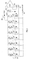
- FIG. 4 is a block diagram of a complete SAR ADC system incorporating programmable input range features in accordance with the present invention, and generally depicted by the numeral 400.
- An analog input signal 401 is applied to one or more capacitors of a CapDAC array 403 through an array of high-voltage switches 402.
- the SAR logic 406 does this based upon range decoder logic 407 that receives a range programming input from a range register 409.
- the range decoder logic 407 is described in greater detail subsequently. It is sufficient for the moment to note that the contents of the range register 409 may be altered by writing to the register over a conventional serial port 410. Allowing the user to access the range register 409 provides a software programming capability for the range of the SAR ADC 400.
- FIG. 5 provides a detailed view of the range decoder logic. Of course, a number of logic implementations would suffice for this application. The implementation of FIG. 5 is simply one satisfactory way of generating a suitable set of ranges for the SAR ADC.
- the decoder itself is an array of NOR gates to which unique combinations of the input signals and their complements are applied. For example, the complement of the Polarity Bit 501, along with the Range1 and Range0 bits are applied to NOR gate 505 in the event that the analog input signal is bipolar with an expected voltage swing between -10 and +10 volts. As illustrated, the input signal is sampled onto the third MSB of the CapDAC array in this case for proper scaling. Unique combinations of the control bits are mapped onto the inputs of different NOR gates so that six different input ranges may be selected for the SAR ADC via software programming.
- FIG. 6 illustrates an alternative embodiment of the invention in which the analog input signal is sampled onto a separate sample array 601, rather than electing to sample directly onto selected capacitors of the CapDAC conversion array 602.
- the selection logic selects one or more elements of the sample array 601 in order to program the range of the SAR ADC.
- the principal advantage of this configuration is that the number of high voltage switches required is substantially reduced. As one would expect, there is an associated saving in die area as well if a separate sampling array is used.
Description
- This invention relates generally to scaling of analog input signals and in particular to scaling both bipolar and unipolar input signals to the dynamic range of an ADC prior to acquisition and conversion, and is more particularly directed toward sampling an analog input signal through high-voltage transmission gates onto a selected combination of sampling capacitors to program the input range of a SAR ADC.
- A successive approximation APC is for example known from
EP0935195 . Multi-input, wide dynamic range bipolar and unipolar successive approximation analog-to-digital converters (ADCs) have traditionally used resistor divider networks at the analog input to scale the input signal to the dynamic range of the converter before acquisition and conversion can take place. This method of attenuating the input signal prior to conversion by the ADC has been used very successfully in the past. However, it has a number of distinct disadvantages. - First of all, in the traditional resistor divider approach the analog input source always sees a resistive load to ground or some reference voltage. The source must be able to drive this load. Second, the resistor divider network consumes power both from the internal reference and from the analog input source. The third problem is that this prior art technique does not allow the user an easy method for programming the allowed analog input range. A fourth disadvantage is the fact that the size of the input resistors will limit the full power bandwidth of the converter.
- The nodes of the resistor network that form the resistor divider can be made accessible to the user via pins on an integrated circuit (IC). The user then configures the resistor divider network via hardware connections to suit the analog input range required. However, if the user wishes to change the range, then the hardware has to be re-wired.
- European Patent Application Publication No.
0 935 195 discloses an integrated circuit with a high resolution analog-to-digital converter, a microcontroller and high density memory and an emulator for an integrated circuit -
US Patent No. 4, 348,658 discloses an analog-to-digital converter using half range technique. - Consequently, a need arises for an analog input voltage scaling technique that is easily adaptable to integrated circuit applications, does not require the input signal to drive a resistive load to ground, minimizes power consumption, and is easily programmable in the event that the allowed analog input voltage range requires alteration.
- These needs and others are satisfied by the programmable input voltage range system and methodology of the present invention as set out in the appended claims, in which a split gate oxide process allows the use of high voltage (±15 volt) switches on the same silicon substrate as standard sub-micron 5 volt CMOS devices. With this process, the analog input voltage can be sampled directly onto the sampling capacitor without the need for prior attenuation circuits. By only sampling on a given ratio of the sampling capacitor, the analog input can be scaled or attenuated to suit the dynamic range of the SAR (successive approximation register) ADC itself.
- In the system of the present invention, the sampling capacitor can be the actual capacitive redistribution digital-to-analog converter (CapDAC) used in the SAR ADC itself, or a separate capacitor array. By selecting which bits of the CapDAC or separate sampling array to sample on, one can program the input range. Once the analog input signal has been attenuated to match the allowed dynamic range of the SAR converter, traditional SAR techniques can be used to convert the input signal to a digital word.
- In this manner, many of the problems of traditional methods are overcome. The analog source sees a capacitive load, not a resistive load to ground - therefore, no DC power is required from the source. Second, no additional power is consumed in biasing a resistor divider network. And last of all, by selecting which bits of the capacitive redistribution DAC or separate sampling array to sample onto, one can program, through software, the analog input range.
- In accordance with one aspect of the present invention, a programmable input voltage range analog-to-digital converter comprises a successive approximation analog-to-digital converter (SAR ADC) having a characteristic dynamic range, and an input voltage scaling network in which the input voltage is sampled onto one or more selected sampling capacitors to scale the input voltage to substantially match the characteristic dynamic range of the SAR ADC. In one form of the invention, the input voltage scaling network is a capacitive redistribution digital-to-analog converter forming a part of the SAR ADC.
- A network of high voltage sampling switches may be interposed between the input voltage and the input voltage scaling network, such that range decoder logic selects one or more elements of the input voltage scaling network on which the input voltage is sampled. The input voltage range may be bipolar.
- In another form of the invention, a network of low-voltage to high-voltage level shifters couples control signals to the high voltage sampling switches. Preferably, the range decoder logic is responsive to a range selection control word written into an associated range register. The range register may be programmable via a digital communication interface. It is preferred that the digital communication interface be a serial, bi-directional communication interface to accommodate both programming of the range register by a user, and read-back of the range register contents for verification, as well as for programming other functionality of the SAR ADC itself.
- In accordance with another aspect of the present invention, a SAR ADC comprises a capacitive redistribution digital-to-analog converter (CapDAC) having an output coupled to a comparator, SAR logic that controls iterative sampling of a SAR ADC input signal and monitors the output of the comparator, an input voltage scaling network in which the input voltage is sampled onto one or more selected sampling capacitors to scale the input voltage to substantially match the characteristic dynamic range of the SAR ADC, a network of high voltage sampling switches interposed between the input voltage and the input voltage scaling network, such that the input voltage is selectively sampled onto one or more of the sampling capacitors, range decoder logic that controls the network of high voltage sampling switches to select one or more of the sampling capacitors, and a range register to which a range selection control word is written, the range decoder logic being responsive to the range selection control word.
- The CapDAC may form at least a part of the input voltage scaling network, and the input voltage may be sampled onto one or more selected sampling capacitors of the CapDAC to scale the input voltage to substantially match the characteristic dynamic range of the SAR ADC. In the alternative, the input voltage scaling network may comprise a network of sampling capacitors independent of the CapDAC array.
- Further objects, features, and advantages of the present invention will become apparent from the following description and drawings.
-
-
FIG. 1 depicts a resistor divider circuit of the prior art used to attenuate analog input signals prior to conversion; -
FIG. 2 illustrates a bipolar analog input signal being sampled onto a CapDAC array in accordance with the principles of the present invention; -
FIG. 3 is a simplified diagram of a switching transistor arrangement suitable for use in the present invention; -
FIG. 4 is a block diagram of a complete SAR ADC incorporating the principles of the present invention; -
FIG. 5 depicts range decoder logic suitable for use with the present invention; and -
FIG. 6 illustrates a sampling array separate from the conversion array in accordance with an alternative embodiment of the present invention. - There is described herein a programmable input range SAR ADC that offers distinct advantages when compared to the prior art.
FIG. 1 illustrates the traditional method used to attenuate wide range bipolar and unipolar analog input signals prior to conversion. A reference voltage Vref, in this example +2.5 volts, is applied to the input of abuffer 102. The buffered reference voltage is applied to the top of a resistor divider formed from resistors R1, R2, and R3. - The analog input signal Ain, which, in this exemplary circuit, ranges between -10 volts and +10 volts, is applied to the
voltage divider input 103. The reference voltage Vref serves as a bias voltage for the voltage divider, with the result that the divider network scales and level-shifts the input signal. The analog input voltage Ain, as it varies from -10 volts to +10 volts, produces a variation at thecommon node 104 from zero volts to +2.5 volts. It is thisoutput node 104, with its scaled output voltage, that is generally coupled to the sample and hold input of a SAR ADC. It should be noted that the analog input signal Ain in this prior art network must drive 40 K (kilohms) to ground. -
FIG. 2 illustrates a bipolar (+10 volt) analog input signal being sampled onto an 8-bit CapDAC array in accordance with the principles of the present invention. The switches to the analog input signal are ±15 volt switches that are capable of directly sampling the bipolar input signal. The switches are described in greater detail below. - It should be noted with respect to
FIG. 2 that the comparator and all the SAR logic of the ADC can be implemented using 5 volt sub-micron CMOS technology. Only the analog input switches are required to be fabricated using ±15 volt CMOS devices that use a thicker gate-oxide to deal with the higher gate voltages required. - The charge equation during sampling for the ±10 volt input range is as follows:

Where Ctot = 256C
That is, the analog input voltage sampled will be:
If Vcom is equal to 1.25 volts, then, for any analog input voltage in the range ±10 volts, the sampled analog input is between 0 volts and 2.5 volts. If the reference voltage is 2.5 volts, then the analog input is kept within the dynamic range of the converter, and the bipolar input signal can be converted using the usual SAR techniques. - In order to program the input range, one simply selects which bits of the CapDAC array to sample onto. This is illustrated for an 8-bit example in Table 1 below:
Input Range MSB B7 B6 B5 B4 B3 B2 B1 LSB B0 Vncp after sampling +10 volts Vref GND Ain GND GND GND GND GND -Ain/8+Vcom ±5 volts Vref Ain GND GND GND GND GND GND -Ain/4+Vcom ±2.5 volts Vref Ain Ain Ain Ain Ain Ain Ain -Ain/2 + V com0 to + 10 v GND Ain GND GND GND GND GND GND -Ain/4+Veom 0 to + 5 v GND Ain Ain Ain Ain Ain Ain Ain -Ain/2 + V com0 to +2.5 v Ain Ain Ain Ain Ain Ain Ain Ain -Ain + Vcom Input Range Polarity Bit Range Bit1 Range Bit0 ±10 volts High Low Low ±5 volts High Low High ±2.5 volts High High High 0 to + 10 v Low Low Low 0 to + 5 v Low Low High 0 to +2.5 v Low High High - It should be noted that for bipolar signals the MSB (the Polarity Bit) is held at the reference voltage during sampling. The reason for this will become apparent later in the description.
- As noted above,
FIG. 2 illustrates a capacitive redistribution DAC, or CapDAC, comprised of a collection of binary weighted capacitors C7 through C0, and a "dummy" capacitor (or terminating capacitor) CD located closest to thecomparator 204. The value of CD is substantially equal to the capacitance of the LSB capacitor C0. In the circuit ofFIG. 2 , the terminating capacitor does not sample the analog input, but is rather held at ground to help with minimizing offsets. The 8-bit capacitor array ofFIG. 2 is shown in sample mode. The total capacitance of the array is 256C, where C is the unit capacitance for the illustrated implementation. - In this exemplary embodiment, the MSB B7 is tied to
Vref 202 during sampling by switch S7, part of the array 207 of analog switches that will be discussed further below. The third most significant bit, B5, is tied to theanalog input voltage 201 through switch S5. When the sampling period is completed, the charge accumulated from the analog input is transferred to the top plate of the capacitor array by switching S5 to ground 208. Thecommon mode switch 206 is opened first so that total charge across the sampling capacitor is conserved. - Thus, in this example, the analog input signal is attenuated by a factor of 8. Therefore, assuming an input signal that varies between +10 and -10 volts, the
comparator 204 actually sees ±1.25 volts. If the commonmode voltage Vcom 203 is 1.25 volts, then the input signal is kept within the common mode range of thecomparator 204. Known successive approximation techniques can then be used to digitize the input signal. - An examination of the MSB bit trial is instructive. As noted previously, the MSB was tied to Vref (2.5 volts) during sampling. Post-sampling, the MSB remains at Vref until a decision is made regarding what to do with the MSB. Just by way of example, if the analog input signal happened to be positive (+10 volts, for example), the voltage at the noninverting input of the comparator (the NCP node 205) would be given by equation (2) above as -Ain/8 + Vcom. In the case where the common mode voltage Vcom is +1.25 volts, then Vncp = 0 volts. The output of
comparator 204 would be a logic LOW level. - One would expect to have the NCP node converge to the common mode voltage. In order to accomplish this, the MSB is left connected to Vref, since switching this point to ground would transfer negative charge to the top plate of the capacitor array and cause the NCP voltage to diverge from the common mode voltage. The SAR logic can be structured to set the first bit of the data output to a logic "1" under these circumstances, since the logic will know that the input is bipolar.
- The second MSB B6 bit trial begins by switching B6 from ground to Vref using switch S6. This transfers a positive charge of weighting Vref/4 to the top plate of the capacitor array. The equation for the
NCP voltage 205 now becomes:
Since the sampled analog input signal in this example was +10 volts, the common mode voltage is +1.25 volts, and the reference voltage Vref is +2.5 volts, the voltage at theNCP node 205 is 0.625 volts. The comparator output is still a logic-LOW, but the NCP voltage is beginning to converge on the common mode voltage. Hence, the second MSB B6 is left tied to Vref and the SAR logic interprets this as a logic "1" and sets the second bit of the data output to "1." The remaining bit trials occur in the same fashion until all 8 bits have been tested and theNCP node 205 is within 1 LSB of the common mode voltage. - In the event that the analog input voltage were negative, the opposite would occur. If an input voltage of -10 volts were applied as the analog input signal, equation (2) above indicates that the NCP node voltage would be 2.5 volts. The comparator output would be a logic HIGH and the SAR logic would interpret this, switch the MSB from Vref to ground, and set the first bit of the data output to a logic "0" For the second MSB bit trial, B6 would be switched to Vref, the NCP node would settle to +1.875 volts, and the comparator output would still be HIGH. The SAR logic would reject this bit by switching it to ground. Thus, the SAR process would continue until the NCP node converges on the common mode voltage. An equation for the NCP voltage during bit trials is given below:

The Vref/2 term (the MSB) has a negative sign and is also multiplied by the inverse ofbit 7. This is because the Vref/2 term is only included when B7 is a logic "0" (i.e., if the actual analog input voltage is negative in polarity). Hence, the MSB behaves like a sign bit. -
FIG. 3 is a simplified diagram of a switching arrangement suitable for use in the present invention. In order to accommodate analog input signals in the range from -10 to +10 volts, a transmission gate is formed from a pair of parallel connected,high voltage PMOS 301 andNMOS 302 transistors. Preferably, the devices illustrated will withstand a 30 volt differential between any two terminals, and provide an adequate safety margin when dealing with input signals in the ±10 volt range. Thehigh voltage devices sampling capacitor 303. Of course, high voltage control signals are required for the gates of thehigh voltage transistors -
FIG. 4 is a block diagram of a complete SAR ADC system incorporating programmable input range features in accordance with the present invention, and generally depicted by the numeral 400. Ananalog input signal 401 is applied to one or more capacitors of aCapDAC array 403 through an array of high-voltage switches 402. TheSAR logic 406, which also controls signal acquisition and conversion in a known manner, controls which capacitors of the CapDAC array the input signal is sampled onto. - The
SAR logic 406 does this based uponrange decoder logic 407 that receives a range programming input from arange register 409. Therange decoder logic 407 is described in greater detail subsequently. It is sufficient for the moment to note that the contents of therange register 409 may be altered by writing to the register over a conventionalserial port 410. Allowing the user to access therange register 409 provides a software programming capability for the range of theSAR ADC 400. -
FIG. 5 provides a detailed view of the range decoder logic. Of course, a number of logic implementations would suffice for this application. The implementation ofFIG. 5 is simply one satisfactory way of generating a suitable set of ranges for the SAR ADC. There are three input signals that control the range of the SAR ADC. These are thePolarity Bit 501, theRange1 Bit 502, and theRange0 Bit 503. Each of these signals is applied to aninverter 504 so that both the signals and their logic complements are available to the decoder section. - The decoder itself is an array of NOR gates to which unique combinations of the input signals and their complements are applied. For example, the complement of the
Polarity Bit 501, along with the Range1 and Range0 bits are applied to NORgate 505 in the event that the analog input signal is bipolar with an expected voltage swing between -10 and +10 volts. As illustrated, the input signal is sampled onto the third MSB of the CapDAC array in this case for proper scaling. Unique combinations of the control bits are mapped onto the inputs of different NOR gates so that six different input ranges may be selected for the SAR ADC via software programming. -
FIG. 6 illustrates an alternative embodiment of the invention in which the analog input signal is sampled onto aseparate sample array 601, rather than electing to sample directly onto selected capacitors of theCapDAC conversion array 602. In this implementation, the selection logic selects one or more elements of thesample array 601 in order to program the range of the SAR ADC. The principal advantage of this configuration is that the number of high voltage switches required is substantially reduced. As one would expect, there is an associated saving in die area as well if a separate sampling array is used. - There has been described herein a programmable input range SAR ADC that offers distinct advantages when compared with the prior art.
Claims (12)
- A programmable input voltage range analog-to-digital- converter (400) comprising:a successive approximation low voltage analog-to-digital converter (SAR ADC) having a characteristic dynamic range;
characterised in that it comprises:an input high voltage scaling network in which the input voltage is a high voltage input signal and is sampled onto one or more selected sampling capacitors to scale the input voltage to substantially match the characteristic dynamic range of the low voltage analog-to-digital converter (SAR ADC), wherein the input high voltage scaling network and the low voltage analog-to-digital converter (SAR ADC) are fabricated on the same silicon substrate. - The programmable input voltage range analog-to- digital converter (400) of claim 1, wherein the input voltage scaling network is a capacitive redistribution digital-to- analog converter (403) forming a part of the low voltage analog-to-digital converter (SAR ADC).
- The programmable input voltage range analog-to- digital converter (400) of claim 1 or claim 2 further comprising a network of high voltage sampling switches (402; 601) interposed between the input voltage and the input high voltage scaling network.
- The programmable input voltage range analog-to- digital converter (400) of claim 2 or claim 3, further comprising range decoder logic (407) that selects one or more elements of the input high voltage scaling network on which the input voltage is sampled.
- The programmable input voltage range analog-to- digital converter (400) of claim 4, wherein the input voltage range is bipolar.
- The programmable input voltage range analog-to-digital converter (400) of claim 5, wherein a network of low-voltage to high-voltage level shifters (405) couples control signals to the high voltage sampling switches (402; 601).
- The programmable input voltage range analog-to-digital converter (400) of claim 4, wherein the range decoder logic (407) is responsive to a range selection control word written into an associated range register (409).
- The programmable input voltage range analog-to-digital converter (400) of claim 7, wherein the range register (409) is programmable via a digital communication interface.
- The programmable input voltage range analog-to-digital converter (400) of claim 8, wherein the digital communication interface is a serial communication interface.
- The programmable input voltage range analog-to-digital converter (400) of claim 9, wherein the serial communication interface is bi-directional.
- The programmable input voltage range analog-to-digital converter of any of the preceding claims, wherein the low voltage analog-to-digital converter is a 5V (SAR ADC).
- The programmable input voltage range analog-to-digital converter of any of the preceding claims, wherein the input voltage is a bipolar analog input signal.
Applications Claiming Priority (3)
| Application Number | Priority Date | Filing Date | Title |
|---|---|---|---|
| US330717 | 1994-10-28 | ||
| US10/330,717 US6731232B1 (en) | 2002-12-27 | 2002-12-27 | Programmable input range SAR ADC |
| PCT/US2003/041264 WO2004062109A1 (en) | 2002-12-27 | 2003-12-24 | Programmable input range sar adc |
Publications (2)
| Publication Number | Publication Date |
|---|---|
| EP1579578A1 EP1579578A1 (en) | 2005-09-28 |
| EP1579578B1 true EP1579578B1 (en) | 2010-02-10 |
Family
ID=32176293
Family Applications (1)
| Application Number | Title | Priority Date | Filing Date |
|---|---|---|---|
| EP03814964A Expired - Lifetime EP1579578B1 (en) | 2002-12-27 | 2003-12-24 | Programmable input range sar adc |
Country Status (7)
| Country | Link |
|---|---|
| US (1) | US6731232B1 (en) |
| EP (1) | EP1579578B1 (en) |
| JP (1) | JP4707396B2 (en) |
| CN (1) | CN1732624B (en) |
| AU (1) | AU2003300374A1 (en) |
| DE (1) | DE60331248D1 (en) |
| WO (1) | WO2004062109A1 (en) |
Cited By (1)
| Publication number | Priority date | Publication date | Assignee | Title |
|---|---|---|---|---|
| EP1728328A1 (en) * | 2004-03-24 | 2006-12-06 | Analog Devices, Inc. | Programmable input range adc |
Families Citing this family (45)
| Publication number | Priority date | Publication date | Assignee | Title |
|---|---|---|---|---|
| US7319423B2 (en) * | 2002-07-31 | 2008-01-15 | Quantum Semiconductor Llc | Multi-mode ADC and its application to CMOS image sensors |
| US7518540B2 (en) * | 2002-07-31 | 2009-04-14 | Quantum Semiconductor Llc | Multi-mode ADC and its application to CMOS image sensors |
| US6828927B1 (en) * | 2002-11-22 | 2004-12-07 | Analog Devices, Inc. | Successive approximation analog-to-digital converter with pre-loaded SAR registers |
| EP1655842A1 (en) | 2004-11-03 | 2006-05-10 | Dialog Semiconductor GmbH | Domino asynchronous successive approximation ADC |
| GB2422258A (en) * | 2005-01-12 | 2006-07-19 | Sharp Kk | Bufferless switched capacitor digital to analogue converter |
| GB2425006A (en) * | 2005-04-05 | 2006-10-11 | Sharp Kk | Switched capacitor digital/analogue converter arrangement |
| JP4751667B2 (en) * | 2005-08-12 | 2011-08-17 | 富士通セミコンダクター株式会社 | Successive comparison AD converter. |
| US7218259B2 (en) * | 2005-08-12 | 2007-05-15 | Analog Devices, Inc. | Analog-to-digital converter with signal-to-noise ratio enhancement |
| JP4803729B2 (en) * | 2006-03-14 | 2011-10-26 | ルネサスエレクトロニクス株式会社 | Semiconductor integrated circuit |
| DE102006015762B4 (en) * | 2006-04-04 | 2013-05-08 | Austriamicrosystems Ag | Analog-to-digital converter arrangement and method |
| DE102006025116B4 (en) * | 2006-05-30 | 2020-06-04 | Austriamicrosystems Ag | Adjustable analog-digital converter arrangement and method for analog-digital conversion |
| US8035622B2 (en) | 2008-03-27 | 2011-10-11 | Apple Inc. | SAR ADC with dynamic input scaling and offset adjustment |
| US7898453B2 (en) * | 2008-12-05 | 2011-03-01 | Qualcomm Incorporated | Apparatus and method for successive approximation analog-to-digital conversion |
| JP2010166298A (en) * | 2009-01-15 | 2010-07-29 | Fujitsu Ltd | Analog-to-digital circuit |
| US8365024B2 (en) * | 2010-02-26 | 2013-01-29 | Honeywell International Inc. | High integrity data bus fault detection using multiple signal components |
| US8054208B2 (en) | 2010-03-30 | 2011-11-08 | Honeywell International Inc. | Re-configurable multipurpose analog interface |
| US8782299B2 (en) | 2010-04-27 | 2014-07-15 | Honeywell International Inc. | Re-configurable multi-purpose digital interface |
| US8237598B2 (en) * | 2010-07-30 | 2012-08-07 | National Instruments Corporation | Sampling of multiple data channels using a successive approximation register converter |
| US8547272B2 (en) * | 2010-08-18 | 2013-10-01 | Analog Devices, Inc. | Charge sharing analog computation circuitry and applications |
| US8390324B2 (en) | 2010-09-20 | 2013-03-05 | Honeywell International Inc. | Universal functionality module |
| US8289198B2 (en) | 2010-11-02 | 2012-10-16 | Texas Instruments Incorporated | Low power bit switches and method for high-voltage input SAR ADC |
| US8587466B2 (en) * | 2011-12-29 | 2013-11-19 | Stmicroelectronics International N.V. | System and method for a successive approximation analog to digital converter |
| CN103513834A (en) * | 2012-06-21 | 2014-01-15 | 瀚宇彩晶股份有限公司 | Sensing circuit of touch panel and method for operating sensing circuit of touch panel |
| CN102832941B (en) * | 2012-10-07 | 2016-03-30 | 复旦大学 | A kind of can the gradual approaching A/D converter of pre-detection comparator input range |
| JP2013059105A (en) * | 2012-11-19 | 2013-03-28 | Fujitsu Ltd | Analog-digital circuit and receiver using the same |
| US8736480B1 (en) * | 2013-01-11 | 2014-05-27 | Intel Corporation | Successive approximation analog-to-digital conversion architectural arrangement for receivers |
| US8766833B1 (en) * | 2013-03-06 | 2014-07-01 | Infineon Technologies Austria Ag | System and method for calibrating a circuit |
| JP6102521B2 (en) * | 2013-05-29 | 2017-03-29 | 株式会社ソシオネクスト | SAR analog-digital conversion method and SAR analog-digital conversion circuit |
| CN104283562A (en) * | 2013-07-12 | 2015-01-14 | 上海明波通信技术股份有限公司 | Successive approximation type analog-to-digital conversion device |
| JP6313018B2 (en) | 2013-11-13 | 2018-04-18 | ルネサスエレクトロニクス株式会社 | Design support device, semiconductor device, and compilation program |
| CN104852736B (en) * | 2014-02-17 | 2018-05-04 | 瑞昱半导体股份有限公司 | Gradual approaching analog-digital converter and conversion method |
| US9281835B2 (en) * | 2014-03-03 | 2016-03-08 | Microsemi Corp.—Analog Mixed Signal Group, Ltd. | Method and apparatus for wide range input for an analog to digital converter |
| CN104253613B (en) * | 2014-09-11 | 2017-06-13 | 电子科技大学 | A kind of low pressure ultra-low-power high-precision comparator of SAR ADC |
| US9473164B1 (en) * | 2015-06-26 | 2016-10-18 | Freescale Semiconductor, Inc. | Method for testing analog-to-digital converter and system therefor |
| CN108476024B (en) * | 2016-09-23 | 2022-01-21 | 深圳市汇顶科技股份有限公司 | DAC capacitor array, SAR analog-to-digital converter and method for reducing power consumption |
| US10270459B2 (en) | 2016-09-23 | 2019-04-23 | Shenzhen GOODIX Technology Co., Ltd. | DAC capacitor array, SAR analog-to-digital converter and method for reducing power consumption thereof |
| KR101972689B1 (en) | 2016-10-25 | 2019-04-25 | 선전 구딕스 테크놀로지 컴퍼니, 리미티드 | How to Reduce DAC Capacitor Arrays and Analog-to-Digital Converters, Analog-to-Digital Converter Power Consumption |
| CN107181490A (en) * | 2016-12-13 | 2017-09-19 | 成都华微电子科技有限公司 | Analog to digital conversion circuit |
| US9793912B1 (en) * | 2016-12-27 | 2017-10-17 | Western Digital Technologies, Inc. | Analog-to-digital conversion circuitry with real-time adjusted gain and resolution |
| EP3432476A4 (en) * | 2017-03-30 | 2019-05-29 | Shenzhen Goodix Technology Co., Ltd. | Analog to digital conversion circuit and method |
| US10084467B1 (en) * | 2018-01-03 | 2018-09-25 | Ncku Research And Development Foundation | ADC and an interfacing circuit adaptable thereto |
| US10574249B2 (en) * | 2018-05-02 | 2020-02-25 | Apple Inc. | Capacitor structure with correlated error mitigation and improved systematic mismatch in technologies with multiple patterning |
| JP7102515B2 (en) | 2018-05-22 | 2022-07-19 | オリンパス株式会社 | Digital-to-analog converters, analog-to-digital converters, signal processing devices, solid-state imaging devices, and driving methods |
| US10447291B1 (en) * | 2018-09-14 | 2019-10-15 | Linear Technology Holding, LLC | High dynamic range analog-to-digital converter |
| TWI672006B (en) * | 2018-09-28 | 2019-09-11 | 新唐科技股份有限公司 | Successive approximation register analog-to-digital converter and control method thereof |
Citations (2)
| Publication number | Priority date | Publication date | Assignee | Title |
|---|---|---|---|---|
| EP0075441A2 (en) * | 1981-09-18 | 1983-03-30 | Fujitsu Limited | Voltage dividing circuit |
| EP0610939A1 (en) * | 1993-02-10 | 1994-08-17 | Nec Corporation | Voltage drop circuit to be built in semiconductor IC chip |
Family Cites Families (13)
| Publication number | Priority date | Publication date | Assignee | Title |
|---|---|---|---|---|
| US4348658A (en) * | 1980-05-09 | 1982-09-07 | Motorola, Inc. | Analog-to-digital converter using half range technique |
| JPS6177430A (en) * | 1984-09-25 | 1986-04-21 | Oki Electric Ind Co Ltd | Analog-digital converter |
| JPH0744457B2 (en) * | 1989-07-17 | 1995-05-15 | 三洋電機株式会社 | A / D converter |
| US5694356A (en) * | 1994-11-02 | 1997-12-02 | Invoice Technology, Inc. | High resolution analog storage EPROM and flash EPROM |
| US5684487A (en) * | 1995-06-05 | 1997-11-04 | Analog Devices, Incorporated | A/D converter with charge-redistribution DAC and split summation of main and correcting DAC outputs |
| US5861831A (en) * | 1996-12-23 | 1999-01-19 | Analog Devices, Inc. | Intermediate frequency (IF) sampling clock-to-clock auto-ranging analog-to-digital converter (ADC) and method |
| JPH10303751A (en) * | 1997-04-22 | 1998-11-13 | Miyagi Oki Denki Kk | Analog/digital converter |
| EP0966792A1 (en) * | 1998-01-20 | 1999-12-29 | Microchip Technology Incorporated | A driver circuit for low voltage operation of a successive approximation register (sar) analog to digital (a/d) converter and method therefor |
| EP0935195A2 (en) * | 1998-02-06 | 1999-08-11 | Analog Devices, Inc. | "An integrated circuit with a high resolution analog-to-digital converter, a microcontroller and high density memory and an emulator for an integrated circuit |
| US6144331A (en) * | 1998-04-08 | 2000-11-07 | Texas Instruments Incorporated | Analog to digital converter with a differential output resistor-digital-to-analog-converter for improved noise reduction |
| DE19936327C2 (en) * | 1999-08-02 | 2003-04-24 | Infineon Technologies Ag | Method and device for carrying out ratiometric measurements using an analog / digital or a digital / analog converter, analog / digital or digital / analog converter, and method for operating an analog / digital or digital / analog converter |
| US6456220B1 (en) * | 2000-06-19 | 2002-09-24 | Cygnal Integrated Products, Inc. | Analog-to-digital converter for processing differential and single-ended inputs |
| US6388589B1 (en) * | 2000-07-17 | 2002-05-14 | Trw Inc. | Programmable video interface |
-
2002
- 2002-12-27 US US10/330,717 patent/US6731232B1/en not_active Expired - Lifetime
-
2003
- 2003-12-24 CN CN2003801078094A patent/CN1732624B/en not_active Expired - Lifetime
- 2003-12-24 AU AU2003300374A patent/AU2003300374A1/en not_active Abandoned
- 2003-12-24 JP JP2004565705A patent/JP4707396B2/en not_active Expired - Fee Related
- 2003-12-24 WO PCT/US2003/041264 patent/WO2004062109A1/en active Application Filing
- 2003-12-24 DE DE60331248T patent/DE60331248D1/de not_active Expired - Lifetime
- 2003-12-24 EP EP03814964A patent/EP1579578B1/en not_active Expired - Lifetime
Patent Citations (2)
| Publication number | Priority date | Publication date | Assignee | Title |
|---|---|---|---|---|
| EP0075441A2 (en) * | 1981-09-18 | 1983-03-30 | Fujitsu Limited | Voltage dividing circuit |
| EP0610939A1 (en) * | 1993-02-10 | 1994-08-17 | Nec Corporation | Voltage drop circuit to be built in semiconductor IC chip |
Cited By (1)
| Publication number | Priority date | Publication date | Assignee | Title |
|---|---|---|---|---|
| EP1728328A1 (en) * | 2004-03-24 | 2006-12-06 | Analog Devices, Inc. | Programmable input range adc |
Also Published As
| Publication number | Publication date |
|---|---|
| US6731232B1 (en) | 2004-05-04 |
| AU2003300374A1 (en) | 2004-07-29 |
| CN1732624A (en) | 2006-02-08 |
| JP4707396B2 (en) | 2011-06-22 |
| JP2006512861A (en) | 2006-04-13 |
| WO2004062109A1 (en) | 2004-07-22 |
| DE60331248D1 (en) | 2010-03-25 |
| CN1732624B (en) | 2010-10-27 |
| EP1579578A1 (en) | 2005-09-28 |
Similar Documents
| Publication | Publication Date | Title |
|---|---|---|
| EP1579578B1 (en) | Programmable input range sar adc | |
| US6940445B2 (en) | Programmable input range ADC | |
| US5841382A (en) | Fast testing of D/A converters | |
| US7903018B2 (en) | Analog/digital converter assembly and corresponding method | |
| US6720903B2 (en) | Method of operating SAR-type ADC and an ADC using the method | |
| JP3748886B2 (en) | Charge redistribution analog-to-digital converter with system calibration | |
| US4803462A (en) | Charge redistribution A/D converter with increased common mode rejection | |
| JP2804269B2 (en) | Redistribution A / D converter and method for converting analog signal to digital signal | |
| US6707403B1 (en) | Analog to digital converter with a calibration circuit for compensating for coupling capacitor errors, and a method for calibrating the analog to digital converter | |
| EP0809889B1 (en) | Analog-to-digital conversion with multiple charge redistribution conversions | |
| US4348658A (en) | Analog-to-digital converter using half range technique | |
| US6130635A (en) | Method of converting an analog signal in an A/D converter utilizing RDAC precharging | |
| JPH06152420A (en) | A/d converter | |
| EP0757862B1 (en) | Low-voltage cmos analog-to-digital converter | |
| US6404376B1 (en) | Capacitor array having reduced voltage coefficient induced non-linearities | |
| US5248974A (en) | Dielectric relaxation correction circuit for charge-redistribution a/d converters | |
| JP3971663B2 (en) | AD converter | |
| US5719576A (en) | Capacitor array digital/analog converter with compensation array for stray capacitance | |
| JP3104952B2 (en) | Analog-to-digital converter and microcomputer equipped with the same | |
| EP0247065B1 (en) | An untrimmed 12 bit monotonic all capacitive a to d converter | |
| JP3896717B2 (en) | Successive comparison A / D converter | |
| JPS649774B2 (en) | ||
| JPH08149009A (en) | Analog-digital converter |
Legal Events
| Date | Code | Title | Description |
|---|---|---|---|
| PUAI | Public reference made under article 153(3) epc to a published international application that has entered the european phase |
Free format text: ORIGINAL CODE: 0009012 |
|
| 17P | Request for examination filed |
Effective date: 20050511 |
|
| AK | Designated contracting states |
Kind code of ref document: A1 Designated state(s): AT BE BG CH CY CZ DE DK EE ES FI FR GB GR HU IE IT LI LU MC NL PT RO SE SI SK TR |
|
| AX | Request for extension of the european patent |
Extension state: AL LT LV MK |
|
| DAX | Request for extension of the european patent (deleted) | ||
| RBV | Designated contracting states (corrected) |
Designated state(s): DE FR GB |
|
| 17Q | First examination report despatched |
Effective date: 20051117 |
|
| GRAP | Despatch of communication of intention to grant a patent |
Free format text: ORIGINAL CODE: EPIDOSNIGR1 |
|
| GRAS | Grant fee paid |
Free format text: ORIGINAL CODE: EPIDOSNIGR3 |
|
| GRAA | (expected) grant |
Free format text: ORIGINAL CODE: 0009210 |
|
| AK | Designated contracting states |
Kind code of ref document: B1 Designated state(s): DE FR GB |
|
| REG | Reference to a national code |
Ref country code: GB Ref legal event code: FG4D |
|
| REF | Corresponds to: |
Ref document number: 60331248 Country of ref document: DE Date of ref document: 20100325 Kind code of ref document: P |
|
| PLBE | No opposition filed within time limit |
Free format text: ORIGINAL CODE: 0009261 |
|
| STAA | Information on the status of an ep patent application or granted ep patent |
Free format text: STATUS: NO OPPOSITION FILED WITHIN TIME LIMIT |
|
| 26N | No opposition filed |
Effective date: 20101111 |
|
| REG | Reference to a national code |
Ref country code: FR Ref legal event code: PLFP Year of fee payment: 13 |
|
| REG | Reference to a national code |
Ref country code: FR Ref legal event code: PLFP Year of fee payment: 14 |
|
| REG | Reference to a national code |
Ref country code: FR Ref legal event code: PLFP Year of fee payment: 15 |
|
| PGFP | Annual fee paid to national office [announced via postgrant information from national office to epo] |
Ref country code: FR Payment date: 20211118 Year of fee payment: 19 Ref country code: GB Payment date: 20211118 Year of fee payment: 19 |
|
| PGFP | Annual fee paid to national office [announced via postgrant information from national office to epo] |
Ref country code: DE Payment date: 20220616 Year of fee payment: 20 |
|
| GBPC | Gb: european patent ceased through non-payment of renewal fee |
Effective date: 20221224 |
|
| PG25 | Lapsed in a contracting state [announced via postgrant information from national office to epo] |
Ref country code: GB Free format text: LAPSE BECAUSE OF NON-PAYMENT OF DUE FEES Effective date: 20221224 |
|
| PG25 | Lapsed in a contracting state [announced via postgrant information from national office to epo] |
Ref country code: FR Free format text: LAPSE BECAUSE OF NON-PAYMENT OF DUE FEES Effective date: 20221231 |
|
| REG | Reference to a national code |
Ref country code: DE Ref legal event code: R071 Ref document number: 60331248 Country of ref document: DE |