JP4803729B2 - Semiconductor integrated circuit - Google Patents
Semiconductor integrated circuit Download PDFInfo
- Publication number
- JP4803729B2 JP4803729B2 JP2006068758A JP2006068758A JP4803729B2 JP 4803729 B2 JP4803729 B2 JP 4803729B2 JP 2006068758 A JP2006068758 A JP 2006068758A JP 2006068758 A JP2006068758 A JP 2006068758A JP 4803729 B2 JP4803729 B2 JP 4803729B2
- Authority
- JP
- Japan
- Prior art keywords
- converter
- integrated circuit
- semiconductor integrated
- external terminal
- sub
- Prior art date
- Legal status (The legal status is an assumption and is not a legal conclusion. Google has not performed a legal analysis and makes no representation as to the accuracy of the status listed.)
- Expired - Fee Related
Links
Images


Classifications
-
- H—ELECTRICITY
- H03—ELECTRONIC CIRCUITRY
- H03M—CODING; DECODING; CODE CONVERSION IN GENERAL
- H03M1/00—Analogue/digital conversion; Digital/analogue conversion
- H03M1/12—Analogue/digital converters
- H03M1/34—Analogue value compared with reference values
- H03M1/38—Analogue value compared with reference values sequentially only, e.g. successive approximation type
- H03M1/46—Analogue value compared with reference values sequentially only, e.g. successive approximation type with digital/analogue converter for supplying reference values to converter
- H03M1/466—Analogue value compared with reference values sequentially only, e.g. successive approximation type with digital/analogue converter for supplying reference values to converter using switched capacitors
-
- H—ELECTRICITY
- H03—ELECTRONIC CIRCUITRY
- H03M—CODING; DECODING; CODE CONVERSION IN GENERAL
- H03M1/00—Analogue/digital conversion; Digital/analogue conversion
- H03M1/66—Digital/analogue converters
- H03M1/68—Digital/analogue converters with conversions of different sensitivity, i.e. one conversion relating to the more significant digital bits and another conversion to the less significant bits
- H03M1/682—Digital/analogue converters with conversions of different sensitivity, i.e. one conversion relating to the more significant digital bits and another conversion to the less significant bits both converters being of the unary decoded type
-
- H—ELECTRICITY
- H03—ELECTRONIC CIRCUITRY
- H03M—CODING; DECODING; CODE CONVERSION IN GENERAL
- H03M1/00—Analogue/digital conversion; Digital/analogue conversion
- H03M1/66—Digital/analogue converters
- H03M1/74—Simultaneous conversion
- H03M1/76—Simultaneous conversion using switching tree
- H03M1/765—Simultaneous conversion using switching tree using a single level of switches which are controlled by unary decoded digital signals
-
- H—ELECTRICITY
- H03—ELECTRONIC CIRCUITRY
- H03M—CODING; DECODING; CODE CONVERSION IN GENERAL
- H03M1/00—Analogue/digital conversion; Digital/analogue conversion
- H03M1/66—Digital/analogue converters
- H03M1/74—Simultaneous conversion
- H03M1/80—Simultaneous conversion using weighted impedances
- H03M1/802—Simultaneous conversion using weighted impedances using capacitors, e.g. neuron-mos transistors, charge coupled devices
- H03M1/804—Simultaneous conversion using weighted impedances using capacitors, e.g. neuron-mos transistors, charge coupled devices with charge redistribution
- H03M1/806—Simultaneous conversion using weighted impedances using capacitors, e.g. neuron-mos transistors, charge coupled devices with charge redistribution with equally weighted capacitors which are switched by unary decoded digital signals
Description
本発明は、入力アナログ信号をディジタル信号に変換する逐次比較型A/D変換器を具備する半導体集積回路に関し、特に逐次比較型A/D変換器に含まれる局部D/A変換器に供給する高精度アナログ基準電圧を半導体集積回路外部から供給する際に有益な技術に関する。 The present invention relates to a semiconductor integrated circuit including a successive approximation A / D converter that converts an input analog signal into a digital signal, and particularly to a local D / A converter included in the successive approximation A / D converter. The present invention relates to a technique useful for supplying a high-precision analog reference voltage from the outside of a semiconductor integrated circuit.
現在、入力アナログ信号をディジタル信号に変換するA/D変換器(アナログ・ディジタル変換器)としては、低コストかつ高性能で製品用途の広い逐次比較型A/D変換器が知られている。 Currently, a low-cost and high-performance successive approximation type A / D converter is widely used as an A / D converter (analog / digital converter) for converting an input analog signal into a digital signal.
逐次比較型A/D変換器では電圧比較器は入力アナログ信号と逐次基準電圧との比較を行い、その比較結果により逐次比較型A/D変換器のコントローラは逐次基準電圧を変更する。電圧比較器は、再度入力アナログ信号との比較を行い、またコントローラは逐次基準電圧を変更すると言う逐次比較が実行される。比較結果による逐次基準電圧の変更に、局部D/A変換器が使用される。比較結果からの複数のビットの制御ディジタル信号に応答して、局部D/A変換器にて逐次基準電圧が変更される。 In the successive approximation A / D converter, the voltage comparator compares the input analog signal with the successive reference voltage, and the controller of the successive approximation A / D converter changes the successive reference voltage according to the comparison result. The voltage comparator performs comparison with the input analog signal again, and the controller performs successive approximation that the sequential reference voltage is changed. A local D / A converter is used to change the successive reference voltage according to the comparison result. In response to a control digital signal of a plurality of bits from the comparison result, the local D / A converter sequentially changes the reference voltage.
この局部D/A変換器としては、下記特許文献1に記載されているように、局部D/A変換器のMSB(Most Significant Bit)側の変換のための主DACに容量アレー型DACを使用する一方、局部D/A変換器のLSB(Least Significant Bit)側の変換のための副DACに抵抗ストリング型DACを使用して半導体集積回路のチップ占有面積を低減することが提案されている。
As this local D / A converter, as described in
この局部D/A変換器の主DACとしての容量アレー型DACは、複数の容量と複数の容量の一端に接続された複数の切り換えスイッチとにより構成され、複数の容量の他端は共通接続され共通接続の電圧は入力アナログ信号と比較される逐次基準電圧として電圧比較器に入力される。複数の切り換えスイッチの各切り換えスイッチの一方の入力端子にはアナログ基準電圧が共通に印加され、複数の切り換えスイッチの各切り換えスイッチの他方の入力端子には基底電圧が共通に印加される。複数の切り換えスイッチは、MSB側の制御ディジタル信号によって制御される。尚、容量アレー型DACの複数の容量に1つの容量が追加され、この1つの追加容量の一端には下記の副DACからのLSB側逐次基準電圧が供給される。 The capacitive array type DAC as the main DAC of the local D / A converter is composed of a plurality of capacitors and a plurality of changeover switches connected to one end of the plurality of capacitors, and the other ends of the plurality of capacitors are connected in common. The voltage of the common connection is input to the voltage comparator as a sequential reference voltage that is compared with the input analog signal. An analog reference voltage is commonly applied to one input terminal of each changeover switch of the plurality of changeover switches, and a base voltage is commonly applied to the other input terminal of each changeover switch of the plurality of changeover switches. The plurality of changeover switches are controlled by a control digital signal on the MSB side. One capacitor is added to the plurality of capacitors of the capacitor array type DAC, and an LSB side sequential reference voltage from the following sub DAC is supplied to one end of the one additional capacitor.
この局部D/A変換器の副DACとしての抵抗ストリング型DACは、直列接続された複数の抵抗と、複数の抵抗の接続ノードに入力端子が接続された複数のスイッチとから構成されている。この複数のスイッチは、LSB側の制御ディジタル信号によって制御される。尚、複数のスイッチの出力端子は共通接続されることによって、共通接続された複数のスイッチの出力端子から副DACからのLSB側逐次基準電圧が生成される。抵抗ストリング型DACの複数の抵抗の直列接続の一端と他端とには、主DACとしての容量アレー型DACと同様に、アナログ基準電圧と基底電圧とがそれぞれ供給されている。 A resistor string type DAC as a sub DAC of the local D / A converter is composed of a plurality of resistors connected in series and a plurality of switches having input terminals connected to connection nodes of the plurality of resistors. The plurality of switches are controlled by a control digital signal on the LSB side. Note that, by connecting the output terminals of the plurality of switches in common, the LSB side sequential reference voltage from the sub DAC is generated from the output terminals of the plurality of commonly connected switches. Analog reference voltage and base voltage are respectively supplied to one end and the other end of the series connection of the plurality of resistors of the resistor string type DAC as in the case of the capacitive array type DAC as the main DAC.
本発明に先立って、本発明者等は、逐次比較型A/D変換器ための局部D/A変換器の主DACとしての容量アレー型DACと副DACとしての抵抗ストリング型DACとに供給されるアナログ基準電圧を半導体集積回路外部の外部電源から供給すると伴に、逐次比較型A/D変換器の電圧比較器とコントローラとにも外部電源から動作電圧を供給することを検討した。 Prior to the present invention, the present inventors supplied a capacitive array type DAC as a main DAC and a resistance string type DAC as a sub DAC of a local D / A converter for a successive approximation type A / D converter. The analog reference voltage is supplied from an external power supply outside the semiconductor integrated circuit, and the operation voltage is also supplied from the external power supply to the voltage comparator and controller of the successive approximation A / D converter.
この検討結果を基に、本発明者等は、局部D/A変換器を含む逐次比較型A/D変換器を内蔵した半導体集積回路を組み込んだマザーボードの評価を行った。 Based on the results of this study, the present inventors evaluated a motherboard incorporating a semiconductor integrated circuit incorporating a successive approximation A / D converter including a local D / A converter.
しかし、この評価の結果、下記の問題が明らかとなった。まず、局部D/A変換器の主DACである容量アレー型DACの複数の切り換えスイッチはMSB側の制御ディジタル信号によって制御されるので、複数の切り換えスイッチの各切り換えスイッチの一方の入力端子のアナログ基準電圧に制御ディジタル信号による切り換えノイズが漏れ込む。この主DACとしての容量アレー型DACのアナログ基準電圧に漏れ込んだ制御ディジタル信号による切り換えノイズが、更に、副DACとしての抵抗ストリング型DACにも漏れ込む危険があると伴に、逐次比較型A/D変換器の電圧比較器とコントローラとにも漏れ込む危険がある。 However, as a result of this evaluation, the following problems became clear. First, since the plurality of changeover switches of the capacitive array type DAC, which is the main DAC of the local D / A converter, is controlled by the control digital signal on the MSB side, the analog of one input terminal of each changeover switch of the plurality of changeover switches Switching noise due to control digital signals leaks into the reference voltage. The switching noise due to the control digital signal leaked into the analog reference voltage of the capacitive array type DAC as the main DAC is further likely to leak into the resistor string type DAC as the sub DAC. There is also a risk of leaking into the voltage comparator and controller of the / D converter.
この危険を回避するためには、半導体集積回路外部の外部電源から抵抗とこの抵抗の両端に接続した一対の容量からなるローパスフィルタの入出力を介して、局部D/A変換器の主DACと副DACとにアナログ基準電圧を供給する。このようにすれば、局部D/A変換器の主DACにアナログ基準電圧に制御ディジタル信号による切り換えノイズが漏れ込んだとしても、ローパスフィルタの入力に漏れ出す切り替えノイズを十分低減できる。その結果、副DACとしての抵抗ストリング型DACと逐次比較型A/D変換器の比較器とコントローラとに漏れ込む切り替えノイズを、十分低減できる。 In order to avoid this danger, the main DAC of the local D / A converter is connected to an external power supply external to the semiconductor integrated circuit via a low-pass filter input / output composed of a resistor and a pair of capacitors connected to both ends of the resistor. An analog reference voltage is supplied to the sub DAC. In this way, even if the switching noise due to the control digital signal leaks to the analog reference voltage in the main DAC of the local D / A converter, the switching noise leaking to the input of the low-pass filter can be sufficiently reduced. As a result, the switching noise leaking into the resistor string type DAC as the sub DAC and the comparator and controller of the successive approximation type A / D converter can be sufficiently reduced.
しかし、ローパスフィルタによる手法は、副DACとしての抵抗ストリング型DACと逐次比較型A/D変換器の比較器とコントローラとに漏れ込む切り替えノイズを十分低減できるが、下記のような別の新たな問題を起こすことが本発明者等による検討により明らかとされた。 However, the low-pass filter method can sufficiently reduce the switching noise leaking into the resistor string type DAC as the sub DAC, the comparator of the successive approximation type A / D converter, and the controller. It has been clarified by examination by the present inventors that a problem occurs.
すなわち、局部D/A変換器の副DACとしての抵抗ストリング型DACで直列接続された複数の抵抗には、アナログ基準電圧から直流電流が流れている。従って、上記のようなローパスフィルタを介して局部D/A変換器の主DACと副DACとにアナログ基準電圧を供給すると、ローパスフィルタの抵抗に副DACの抵抗ストリング型DACの直流電流による電圧降下が発生する。このローパスフィルタの抵抗における電圧降下は、局部D/A変換器の主DACと副DACとに供給されるアナログ基準電圧の精度に悪影響を与える。 That is, a direct current flows from the analog reference voltage through a plurality of resistors connected in series by a resistor string type DAC as a sub DAC of the local D / A converter. Therefore, when an analog reference voltage is supplied to the main DAC and the sub DAC of the local D / A converter through the low-pass filter as described above, the voltage drop due to the DC current of the resistor string type DAC of the sub-DAC is caused to the resistance of the low-pass filter. Will occur. This voltage drop in the resistance of the low-pass filter adversely affects the accuracy of the analog reference voltage supplied to the main DAC and the sub DAC of the local D / A converter.
前記特許文献1には、局部D/A変換器の主DACである容量アレー型DACの複数の切り換えスイッチの一方の入力端子にアナログ基準電圧を供給する一方、局部D/A変換器の副DACとしての抵抗ストリング型DACに電圧フォロワー回路を介してアナログ基準電圧を供給するが記載されている。しかし、この方法では、電圧フォロワー回路に供給されたアナログ基準電圧よりも更に高い電圧が電圧フォロワー回路の動作電源電圧として必要となる。
In
従って、本発明は、上記のような本発明者等による検討結果を基にしてなされたものである。従って、本発明の目的とするところは、半導体集積回路に内蔵された逐次型A/D変換器のための局部D/A変換器の主DACの複数の容量に接続された複数の切り換えスイッチの一方の入力端子に半導体集積回路の外部からローパスフィルターの入出力を介してアナログ基準電圧を供給しても、局部D/A変換器の副DACとしての抵抗ストリング型DACの直流電流による直流電圧降下がローパスフィルターの抵抗で生じることを回避することにある。 Therefore, the present invention has been made on the basis of the results of the study by the present inventors as described above. Accordingly, an object of the present invention is to provide a plurality of changeover switches connected to a plurality of capacitors of a main DAC of a local D / A converter for a sequential A / D converter built in a semiconductor integrated circuit. Even if an analog reference voltage is supplied to the one input terminal from the outside of the semiconductor integrated circuit through the input / output of the low-pass filter, the DC voltage drop due to the DC current of the resistor string type DAC as the sub DAC of the local D / A converter Is to avoid the occurrence of the low-pass filter resistance.
本発明の前記並びにその他の目的と新規な特徴とは、本明細書の記述及び添付図面から明らかになるであろう。 The above and other objects and novel features of the present invention will be apparent from the description of this specification and the accompanying drawings.
本願において開示される発明のうち代表的なものの概要を簡単に説明すれば、下記の通りである。 The outline of a typical invention among the inventions disclosed in the present application will be briefly described as follows.
すなわち、本発明のひとつの形態による半導体集積回路は、局部D/A変換器を含む逐次比較型A/D変換器を内蔵してなる。局部D/A変換器の主D/A変換器と副D/A変換器とは、それぞれ容量アレー型D/A変換器と抵抗ストリング型D/A変換器とで構成されている。主D/A変換器としての容量アレー型D/A変換器は、複数の容量(C0、C1…C254)と、複数の容量(C0、C1…C254)の一端に接続された複数の切り換えスイッチ(CSW0、CSW1…CSW254)とにより構成され、複数の容量(C0、C1…C254)の他端は共通接続され共通接続の電圧(Vx)は入力アナログ信号(Analog In)と比較される逐次基準電圧として電圧比較器(Comp)に入力される。複数の切り換えスイッチ(CSW0、CSW1…CSW254)の各切り換えスイッチの一方の入力端子に半導体集積回路外部からローパスフィルター(LPF1)を介してアナログ基準電圧(AVrefhigh)が共通に供給可能なように、複数の切り換えスイッチ(CSW0、CSW1…CSW254)の各切り換えスイッチの一方の入力端子は半導体集積回路の第1外部端子(T1)に共通に接続されている。容量アレー型D/A変換器の前記複数の容量(C0、C1…C254)には1つの容量(C255)が追加され、この1つの追加容量(C255)の一端には下記の副D/A変換器からのLSB側逐次基準電圧が供給される。局部D/A変換器の副D/A変換器としての抵抗ストリング型D/A変換器は、直列接続された複数の抵抗(R15、R14…R1、R0)と、複数の抵抗(R15、R14…R1、R0)の接続ノードに入力端子が接続された複数のスイッチ(RSW15、RSW14…RSW01、RSW00)とから構成されている。複数のスイッチ(RSW15、RSW14…RSW01、RSW00)の出力端子は共通接続されることによって、共通接続された複数のスイッチ(RSW15、RSW14…RSW01、RSW00)の出力端子から副D/A変換器からのLSB側逐次基準電圧が生成される。副D/A変換器としての抵抗ストリング型D/A変換器の複数の抵抗(R15、R14…R1、R0)の直列接続の一端には半導体集積回路外部から前記アナログ基準電圧(AVcc)が供給可能なように、前記複数の抵抗(R15、R14…R1、R0)の前記直列接続の前記一端は半導体集積回路の第2外部端子(T2)に接続されている(図1参照)。 That is, a semiconductor integrated circuit according to one embodiment of the present invention includes a successive approximation type A / D converter including a local D / A converter. The main D / A converter and the sub D / A converter of the local D / A converter are respectively composed of a capacitance array type D / A converter and a resistor string type D / A converter. A capacitive array type D / A converter as a main D / A converter includes a plurality of capacitors (C0, C1,... C254) and a plurality of changeover switches connected to one end of the plurality of capacitors (C0, C1,... C254). (CSW0, CSW1... CSW254), the other ends of the plurality of capacitors (C0, C1... C254) are commonly connected, and the voltage (Vx) of the common connection is compared with the input analog signal (Analog In). The voltage is input to the voltage comparator (Comp). A plurality of changeover switches (CSW0, CSW1,..., CSW254) are connected to one input terminal of each changeover switch so that the analog reference voltage (AVrefhigh) can be commonly supplied from the outside of the semiconductor integrated circuit via a low pass filter (LPF1). One input terminal of each change-over switch (CSW0, CSW1,... CSW254) is commonly connected to the first external terminal (T1) of the semiconductor integrated circuit. One capacitor (C255) is added to the plurality of capacitors (C0, C1... C254) of the capacitor array type D / A converter, and the following sub D / A is provided at one end of the one additional capacitor (C255). The LSB side sequential reference voltage from the converter is supplied. A resistor string type D / A converter as a sub D / A converter of the local D / A converter includes a plurality of resistors (R15, R14... R1, R0) connected in series and a plurality of resistors (R15, R14). ... R1, R0) and a plurality of switches (RSW15, RSW14 ... RSW01, RSW00) having input terminals connected to the connection node. The output terminals of the plurality of switches (RSW15, RSW14... RSW01, RSW00) are connected in common, so that the sub D / A converters output from the output terminals of the plurality of commonly connected switches (RSW15, RSW14... RSW01, RSW00). LSB side successive reference voltages are generated. The analog reference voltage (AVcc) is supplied from the outside of the semiconductor integrated circuit to one end of a series connection of a plurality of resistors (R15, R14... R1, R0) of a resistor string type D / A converter as a sub D / A converter. As possible, the one end of the series connection of the plurality of resistors (R15, R14... R1, R0) is connected to a second external terminal (T2) of the semiconductor integrated circuit (see FIG. 1).
本発明のひとつの形態の手段によれば、副D/A変換器としての抵抗ストリング型D/A変換器の複数の抵抗(R15、R14…R1、R0)の直列接続の前記一端は半導体集積回路の第2外部端子(T2)に接続されているので、主D/A変換器としての容量アレー型D/A変換器の複数の切り換えスイッチ(CSW0、CSW1…CSW254)の一方の入力端子に半導体集積回路外部からローパスフィルター(LPF1)を介してアナログ基準電圧(AVrefhigh)を共通に供給しても、局部D/A変換器の副DACとしての抵抗ストリング型DACの直流電流による直流電圧降下がローパスフィルター(LPF1)の抵抗(10Ω)で生じることを回避することができる(図1参照)。 According to one aspect of the present invention, the one end of the series connection of a plurality of resistors (R15, R14... R1, R0) of a resistor string type D / A converter as a sub D / A converter is integrated in a semiconductor integrated circuit. Since it is connected to the second external terminal (T2) of the circuit, it is connected to one input terminal of a plurality of changeover switches (CSW0, CSW1,... CSW254) of a capacitive array type D / A converter as a main D / A converter. Even if the analog reference voltage (AVrefhigh) is commonly supplied from the outside of the semiconductor integrated circuit via the low-pass filter (LPF1), the DC voltage drop due to the DC current of the resistor string type DAC as the sub DAC of the local D / A converter is reduced. It is possible to avoid the occurrence of a resistance (10Ω) of the low-pass filter (LPF1) (see FIG. 1).
本発明のひとつの具体的な形態では、前記半導体集積回路の前記第1外部端子(T1)に前記半導体集積回路外部からローパスフィルター(LPF1)を介して前記アナログ基準電圧(AVrefhigh)が供給され、前記半導体集積回路の前記第2外部端子(T2)に前記半導体集積回路外部から前記アナログ基準電圧(AVrefhigh)が供給される。 In one specific form of the present invention, the analog reference voltage (AVrefhigh) is supplied to the first external terminal (T1) of the semiconductor integrated circuit from the outside of the semiconductor integrated circuit via a low pass filter (LPF1), The analog reference voltage (AVrefhigh) is supplied from the outside of the semiconductor integrated circuit to the second external terminal (T2) of the semiconductor integrated circuit.
本発明の他のひとつの形態による半導体集積回路も、局部D/A変換器を含む逐次比較型A/D変換器を内蔵してなる。局部D/A変換器の主D/A変換器と副D/A変換器とは、それぞれ、容量アレー型D/A変換器と抵抗ストリング型D/A変換器とで構成されている。主D/A変換器としての容量アレー型D/A変換器は、複数の容量(C0、C1…C254)と、複数の容量(C0、C1…C254)の一端に接続された複数の切り換えスイッチ(CSW0、CSW1…CSW254)とにより構成され、複数の容量(C0、C1…C254)の他端は共通接続され共通接続の電圧(Vx)は入力アナログ信号(Analog In)と比較される逐次基準電圧として電圧比較器(Comp)に入力される。複数の切り換えスイッチ(CSW0、CSW1…CSW254)の各切り換えスイッチの一方の入力端子に半導体集積回路外部からローパスフィルター(LPF1)を介してアナログ基準電圧(AVrefhigh)が共通に供給可能なように、複数の切り換えスイッチ(CSW0、CSW1…CSW254)の各切り換えスイッチの一方の入力端子は半導体集積回路の第1外部端子(T1)に共通に接続されている。容量アレー型D/A変換器では、前記複数の容量(C0、C1…C254)に1つの容量(C255)が追加され、この1つの追加容量(C255)の一端には下記の副D/A変換器からのLSB側逐次基準電圧が供給される。局部D/A変換器の副D/A変換器としての抵抗ストリング型D/A変換器は、直列接続された複数の抵抗(R15、R14…R1、R0)と、複数の抵抗(R15、R14…R1、R0)の接続ノードに入力端子が接続された複数のスイッチ(RSW15、RSW14…RSW01、RSW00)とから構成されている。複数のスイッチ(RSW15、RSW14…RSW01、RSW00)の出力端子は共通接続されることによって、共通接続された複数のスイッチ(RSW15、RSW14…RSW01、RSW00)の出力端子から副D/A変換器からのLSB側逐次基準電圧が生成される。副D/A変換器としての抵抗ストリング型D/A変換器の複数の抵抗(R15、R14…R1、R0)の直列接続の一端には半導体集積回路外部から前記アナログ基準電圧(AVcc)が供給可能なように、前記複数の抵抗(R15、R14…R1、R0)の前記直列接続の前記一端の接続先は前記第1外部端子(T1)から半導体集積回路の第2外部端子(T2)に切り替え可能とされている(図2参照)。 A semiconductor integrated circuit according to another embodiment of the present invention also includes a successive approximation A / D converter including a local D / A converter. The main D / A converter and the sub D / A converter of the local D / A converter are respectively composed of a capacitance array type D / A converter and a resistor string type D / A converter. A capacitive array type D / A converter as a main D / A converter includes a plurality of capacitors (C0, C1,... C254) and a plurality of changeover switches connected to one end of the plurality of capacitors (C0, C1,... C254). (CSW0, CSW1... CSW254), the other ends of the plurality of capacitors (C0, C1... C254) are commonly connected, and the voltage (Vx) of the common connection is compared with the input analog signal (Analog In). The voltage is input to the voltage comparator (Comp). A plurality of changeover switches (CSW0, CSW1,..., CSW254) are connected to one input terminal of each changeover switch so that the analog reference voltage (AVrefhigh) can be commonly supplied from the outside of the semiconductor integrated circuit via a low pass filter (LPF1). One input terminal of each change-over switch (CSW0, CSW1,... CSW254) is commonly connected to the first external terminal (T1) of the semiconductor integrated circuit. In the capacitor array type D / A converter, one capacitor (C255) is added to the plurality of capacitors (C0, C1,... C254), and one of the additional capacitors (C255) has one of the following sub D / A converters. The LSB side sequential reference voltage from the converter is supplied. A resistor string type D / A converter as a sub D / A converter of the local D / A converter includes a plurality of resistors (R15, R14... R1, R0) connected in series and a plurality of resistors (R15, R14). ... R1, R0) and a plurality of switches (RSW15, RSW14 ... RSW01, RSW00) having input terminals connected to the connection node. The output terminals of the plurality of switches (RSW15, RSW14... RSW01, RSW00) are connected in common, so that the sub D / A converters output from the output terminals of the plurality of commonly connected switches (RSW15, RSW14... RSW01, RSW00). LSB side successive reference voltages are generated. The analog reference voltage (AVcc) is supplied from the outside of the semiconductor integrated circuit to one end of a series connection of a plurality of resistors (R15, R14... R1, R0) of a resistor string type D / A converter as a sub D / A converter. As possible, the connection destination of the one end of the series connection of the plurality of resistors (R15, R14... R1, R0) is from the first external terminal (T1) to the second external terminal (T2) of the semiconductor integrated circuit. Switching is possible (see FIG. 2).
本発明の他のひとつの形態の手段によれば、副D/A変換器としての抵抗ストリング型D/A変換器の複数の抵抗(R15、R14…R1、R0)の直列接続の前記一端の接続先は前記第1外部端子(T1)から前記第2外部端子(T2)に切り替え可能とされているので、主D/A変換器としての容量アレー型D/A変換器の複数の切り換えスイッチ(CSW0、CSW1…CSW254)の一方の入力端子に半導体集積回路外部からローパスフィルター(LPF1)を介してアナログ基準電圧(AVrefhigh)を共通に供給しても、局部D/A変換器の副DACとしての抵抗ストリング型DACの直流電流による直流電圧降下がローパスフィルター(LPF1)の抵抗(10Ω)で生じることを回避することができる(図2参照)。 According to another aspect of the invention, the one end of the series connection of a plurality of resistors (R15, R14... R1, R0) of a resistor string type D / A converter as a sub D / A converter is provided. Since the connection destination can be switched from the first external terminal (T1) to the second external terminal (T2), a plurality of changeover switches of a capacitive array type D / A converter as a main D / A converter Even if the analog reference voltage (AVrefhigh) is commonly supplied from one outside of the semiconductor integrated circuit to the one input terminal of (CSW0, CSW1... CSW254) via the low pass filter (LPF1), it is used as a sub DAC of the local D / A converter. It can be avoided that a DC voltage drop due to the DC current of the resistor string type DAC is caused by the resistance (10Ω) of the low pass filter (LPF1) (see FIG. 2).
本発明の他のひとつの形態による半導体集積回路では、前記副D/A変換器としての前記抵抗ストリング型D/A変換器の前記複数の抵抗(R15、R14…R1、R0)の前記直列接続の前記一端は第1のPチャンネルMOSトランジスタ(Mp1)のドレイン・ソース電流経路を介して前記半導体集積回路の前記第1外部端子(T1)に接続され、前記副D/A変換器としての前記抵抗ストリング型D/A変換器の前記複数の抵抗(R15、R14…R1、R0)の前記直列接続の前記一端は第2のPチャンネルMOSトランジスタ(Mp2)のドレイン・ソース電流経路を介して前記半導体集積回路の前記第2外部端子(T2)に接続され、前記第1のPチャンネルMOSトランジスタ(Mp1)をオフ状態に前記第2のPチャンネルMOSトランジスタ(Mp2)をオン状態に制御することにより、前記複数の抵抗(R15、R14…R1、R0)の前記直列接続の前記一端の前記接続先を前記第1外部端子(T1)から前記第2外部端子(T2)に切り替えるものである(図2参照)。 In a semiconductor integrated circuit according to another embodiment of the present invention, the series connection of the plurality of resistors (R15, R14... R1, R0) of the resistor string type D / A converter as the sub D / A converter. Is connected to the first external terminal (T1) of the semiconductor integrated circuit via the drain / source current path of the first P-channel MOS transistor (Mp1), and the sub-D / A converter serves as the sub-D / A converter. The one end of the series connection of the plurality of resistors (R15, R14... R1, R0) of the resistor string type D / A converter is connected via the drain / source current path of the second P-channel MOS transistor (Mp2). The second P-channel is connected to the second external terminal (T2) of the semiconductor integrated circuit and turns off the first P-channel MOS transistor (Mp1). By controlling the OS transistor (Mp2) to be in an on state, the connection destination of the one end of the series connection of the plurality of resistors (R15, R14... R1, R0) is connected to the first external terminal (T1). 2 is switched to the external terminal (T2) (see FIG. 2).
本発明の他のひとつの形態による半導体集積回路では、前記第1のPチャンネルMOSトランジスタ(Mp1)をオフ状態に前記第2のPチャンネルMOSトランジスタ(Mp2)をオン状態に制御する制御プログラムを内蔵メモリ(ROM、NV_Flash)に格納したものである(図2参照)。 In a semiconductor integrated circuit according to another embodiment of the present invention, a control program for controlling the first P-channel MOS transistor (Mp1) to an off state and the second P-channel MOS transistor (Mp2) to an on state is incorporated. It is stored in a memory (ROM, NV_Flash) (see FIG. 2).
本発明の更に他のひとつの形態による半導体集積回路は、局部D/A変換器を含む逐次比較型A/D変換器を内蔵してなる。局部D/A変換器の主D/A変換器と副D/A変換器とは、それぞれ容量アレー型D/A変換器と電流切り換え型D/A変換器とで構成されている。主D/A変換器としての容量アレー型D/A変換器は、複数の容量(C0、C1…C254)と、複数の容量(C0、C1…C254)の一端に接続された複数の切り換えスイッチ(CSW0、CSW1…CSW254)とにより構成され、複数の容量(C0、C1…C254)の他端は共通接続され共通接続の電圧(Vx)は入力アナログ信号と比較される逐次基準電圧として電圧比較器(Comp)に入力される。複数の切り換えスイッチ(CSW0、CSW1…CSW254)の各切り換えスイッチの一方の入力端子に半導体集積回路外部からローパスフィルター(LPF1)を介してアナログ基準電圧(AVrefhigh)が共通に供給可能なように、複数の切り換えスイッチ(CSW0、CSW1…CSW254)の各切り換えスイッチの一方の入力端子は半導体集積回路の第1外部端子(T1)に共通に接続されている。容量アレー型D/A変換器の前記複数の容量(C0、C1…C254)には1つの容量(C255)が追加され、この1つの追加容量(C255)の一端には下記の副D/A変換器からのLSB側逐次基準電圧が供給される。局部D/A変換器の副D/A変換器としての電流切り換え型D/A変換器は、所定の比率で重み付けされた複数の定電流源(I0、2IO…16IO)と、この複数の定電流源(I0、2IO…16IO)にそれぞれ接続された複数の差動対トランジスタ(Qp1、Qp2;Qp3、Qp4;…;Qp5、Qp6)から構成されている。複数の差動対トランジスタの一方の複数のトランジスタ(Qp1;Qp3;…;Qp5)の出力端子は共通接続されることによって、共通接続された一方の複数のトランジスタ(Qp1;Qp3;…;Qp5)の出力端子から副D/A変換器からのLSB側逐次基準電圧が生成される。副D/A変換器としての電流切り換え型D/A変換器の複数の定電流源(I0、2IO…16IO)には半導体集積回路外部からアナログ基準電圧(AVcc)が供給可能なように、副D/A変換器としての電流切り換え型D/A変換器の複数の定電流源(I0、2IO…16IO)は半導体集積回路の第2外部端子(T2)に接続されている(図3参照)。 A semiconductor integrated circuit according to still another embodiment of the present invention includes a successive approximation A / D converter including a local D / A converter. The main D / A converter and the sub D / A converter of the local D / A converter are respectively composed of a capacitance array type D / A converter and a current switching type D / A converter. A capacitive array type D / A converter as a main D / A converter includes a plurality of capacitors (C0, C1,... C254) and a plurality of changeover switches connected to one end of the plurality of capacitors (C0, C1,... C254). (CSW0, CSW1... CSW254), the other ends of the plurality of capacitors (C0, C1... C254) are connected in common, and the voltage of the common connection (Vx) is a voltage comparison as a sequential reference voltage compared with the input analog signal. Is input to a device (Comp). A plurality of changeover switches (CSW0, CSW1,..., CSW254) are connected to one input terminal of each changeover switch so that the analog reference voltage (AVrefhigh) can be commonly supplied from the outside of the semiconductor integrated circuit via a low pass filter (LPF1). One input terminal of each change-over switch (CSW0, CSW1,... CSW254) is commonly connected to the first external terminal (T1) of the semiconductor integrated circuit. One capacitor (C255) is added to the plurality of capacitors (C0, C1... C254) of the capacitor array type D / A converter, and the following sub D / A is provided at one end of the one additional capacitor (C255). The LSB side sequential reference voltage from the converter is supplied. A current switching type D / A converter as a sub D / A converter of the local D / A converter includes a plurality of constant current sources (I 0 , 2I O ... 16I O ) weighted at a predetermined ratio, It comprises a plurality of differential pair transistors (Qp1, Qp2; Qp3, Qp4;...; Qp5, Qp6) connected to a plurality of constant current sources (I 0 , 2I O ... 16I O ), respectively. The output terminals of one of the plurality of differential pair transistors (Qp1; Qp3;...; Qp5) are connected in common, so that one of the plurality of commonly connected transistors (Qp1; Qp3;...; Qp5) LSB side successive reference voltage from the sub D / A converter is generated from the output terminal of the sub-D / A converter. An analog reference voltage (AVcc) can be supplied from the outside of the semiconductor integrated circuit to a plurality of constant current sources (I 0 , 2I O ... 16I O ) of the current switching type D / A converter as the sub D / A converter. In addition, a plurality of constant current sources (I 0 , 2I O ... 16I O ) of the current switching type D / A converter as the sub D / A converter are connected to the second external terminal (T2) of the semiconductor integrated circuit. (See FIG. 3).
本発明の更に他のひとつの形態の手段によれば、副D/A変換器としての電流切り換え型D/A変換器の複数の定電流源(I0、2IO…16IO)は半導体集積回路の第2外部端子(T2)に接続されているので、主D/A変換器としての容量アレー型D/A変換器の複数の切り換えスイッチ(CSW0、CSW1…CSW254)の各切り換えスイッチの一方の入力端子に半導体集積回路外部からローパスフィルター(LPF1)を介してアナログ基準電圧(AVrefhigh)を共通に供給しても、局部D/A変換器の副D/A変換器としての電流切り換え型D/A変換器の直流電流による直流電圧降下がローパスフィルター(LPF1)の抵抗(10Ω)で生じることを回避することができる(図3参照)。 According to still another mode of the present invention, a plurality of constant current sources (I 0 , 2I O ... 16I O ) of a current switching type D / A converter as a sub D / A converter are integrated in a semiconductor integrated circuit. Since it is connected to the second external terminal (T2) of the circuit, one of the changeover switches of the plurality of changeover switches (CSW0, CSW1,... CSW254) of the capacitive array type D / A converter as the main D / A converter. Even if the analog reference voltage (AVrefhigh) is commonly supplied to the input terminal of the local D / A converter from the outside of the semiconductor integrated circuit via the low pass filter (LPF1), the current switching type D as the sub D / A converter of the local D / A converter A DC voltage drop due to the DC current of the / A converter can be avoided from occurring in the resistance (10Ω) of the low-pass filter (LPF1) (see FIG. 3).
本発明の更に他のひとつの形態では、前記半導体集積回路の前記第1外部端子(T1)に前記半導体集積回路外部からローパスフィルター(LPF1)を介して前記アナログ基準電圧(AVrefhigh)が供給され、前記半導体集積回路の前記第2外部端子(T2)に前記半導体集積回路外部から前記アナログ基準電圧(AVrefhigh)が供給される。 In still another embodiment of the present invention, the analog reference voltage (AVrefhigh) is supplied from the outside of the semiconductor integrated circuit to the first external terminal (T1) of the semiconductor integrated circuit via a low pass filter (LPF1). The analog reference voltage (AVrefhigh) is supplied from the outside of the semiconductor integrated circuit to the second external terminal (T2) of the semiconductor integrated circuit.
本発明の更に他のひとつの形態による半導体集積回路は、局部D/A変換器を含む逐次比較型A/D変換器を内蔵してなる。局部D/A変換器の主D/A変換器と副D/A変換器とは、それぞれ容量アレー型D/A変換器と電流切り換え型D/A変換器とで構成されている。主D/A変換器としての容量アレー型D/A変換器は、複数の容量(C0、C1…C254)と、複数の容量(C0、C1…C254)の一端に接続された複数の切り換えスイッチ(CSW0、CSW1…CSW254)とにより構成され、複数の容量(C0、C1…C254)の他端は共通接続され共通接続の電圧(Vx)は入力アナログ信号と比較される逐次基準電圧として電圧比較器(Comp)に入力される。複数の切り換えスイッチ(CSW0、CSW1…CSW254)の各切り換えスイッチの一方の入力端子に半導体集積回路外部からローパスフィルター(LPF1)を介してアナログ基準電圧(AVrefhigh)が共通に供給可能なように、複数の切り換えスイッチ(CSW0、CSW1…CSW254)の各切り換えスイッチの一方の入力端子は半導体集積回路の第1外部端子(T1)に共通に接続されている。容量アレー型D/A変換器の前記複数の容量(C0、C1…C254)には1つの容量(C255)が追加され、この1つの追加容量(C255)の一端には下記の副D/A変換器からのLSB側逐次基準電圧が供給される。局部D/A変換器の副D/A変換器としての電流切り換え型D/A変換器は、所定の比率で重み付けされた複数の定電流源(I0、2IO…16IO)と、この複数の定電流源(I0、2IO…16IO)にそれぞれ接続された複数の差動対トランジスタ(Qp1、Qp2;Qp3、Qp4;…;Qp5、Qp6)から構成されている。複数の差動対トランジスタの一方の複数のトランジスタ(Qp1;Qp3;…;Qp5)の出力端子は共通接続されることによって、共通接続された一方の複数のトランジスタ(Qp1;Qp3;…;Qp5)の出力端子から副D/A変換器からのLSB側逐次基準電圧が生成される。副D/A変換器としての電流切り換え型D/A変換器の複数の定電流源(I0、2IO…16IO)には半導体集積回路外部からアナログ基準電圧(AVcc)が供給可能なように、副D/A変換器としての電流切り換え型D/A変換器の複数の定電流源(I0、2IO…16IO)の接続先が前記第1外部端子(T1)から半導体集積回路の第2外部端子(T2)に切り替え可能とされている(図4参照)。 A semiconductor integrated circuit according to still another embodiment of the present invention includes a successive approximation A / D converter including a local D / A converter. The main D / A converter and the sub D / A converter of the local D / A converter are respectively composed of a capacitance array type D / A converter and a current switching type D / A converter. A capacitive array type D / A converter as a main D / A converter includes a plurality of capacitors (C0, C1,... C254) and a plurality of changeover switches connected to one end of the plurality of capacitors (C0, C1,... C254). (CSW0, CSW1... CSW254), the other ends of the plurality of capacitors (C0, C1... C254) are connected in common, and the voltage of the common connection (Vx) is a voltage comparison as a sequential reference voltage compared with the input analog signal. Is input to a device (Comp). A plurality of changeover switches (CSW0, CSW1,..., CSW254) are connected to one input terminal of each changeover switch so that the analog reference voltage (AVrefhigh) can be commonly supplied from the outside of the semiconductor integrated circuit via a low pass filter (LPF1). One input terminal of each change-over switch (CSW0, CSW1,... CSW254) is commonly connected to the first external terminal (T1) of the semiconductor integrated circuit. One capacitor (C255) is added to the plurality of capacitors (C0, C1... C254) of the capacitor array type D / A converter, and the following sub D / A is provided at one end of the one additional capacitor (C255). The LSB side sequential reference voltage from the converter is supplied. A current switching type D / A converter as a sub D / A converter of the local D / A converter includes a plurality of constant current sources (I 0 , 2I O ... 16I O ) weighted at a predetermined ratio, It comprises a plurality of differential pair transistors (Qp1, Qp2; Qp3, Qp4;...; Qp5, Qp6) connected to a plurality of constant current sources (I 0 , 2I O ... 16I O ), respectively. The output terminals of one of the plurality of differential pair transistors (Qp1; Qp3;...; Qp5) are connected in common, so that one of the plurality of commonly connected transistors (Qp1; Qp3;...; Qp5) LSB side successive reference voltage from the sub D / A converter is generated from the output terminal of the sub-D / A converter. An analog reference voltage (AVcc) can be supplied from the outside of the semiconductor integrated circuit to a plurality of constant current sources (I 0 , 2I O ... 16I O ) of the current switching type D / A converter as the sub D / A converter. In addition, a connection destination of a plurality of constant current sources (I 0 , 2I O ... 16I O ) of the current switching type D / A converter as the sub D / A converter is connected to the semiconductor integrated circuit from the first external terminal (T1). The second external terminal (T2) can be switched (see FIG. 4).
本発明の更に他のひとつの形態の手段によれば、副D/A変換器としての電流切り換え型D/A変換器の複数の定電流源(I0、2IO…16IO)の接続先が前記第1外部端子(T1)から前記第2外部端子(T2)に切り替え可能とされているので、主D/A変換器としての容量アレー型D/A変換器の複数の切り換えスイッチ(CSW0、CSW1…CSW254)の各切り換えスイッチの一方の入力端子に半導体集積回路外部からローパスフィルター(LPF1)を介してアナログ基準電圧(AVrefhigh)を共通に供給しても、局部D/A変換器の副D/A変換器としての電流切り換え型D/A変換器の直流電流による直流電圧降下がローパスフィルター(LPF1)の抵抗(10Ω)で生じることを回避することができる(図4参照)。 According to still another mode of the present invention, the connection destinations of a plurality of constant current sources (I 0 , 2I O ... 16I O ) of a current switching type D / A converter as a sub D / A converter. Can be switched from the first external terminal (T1) to the second external terminal (T2). Therefore, a plurality of changeover switches (CSW0) of a capacitive array type D / A converter as a main D / A converter are provided. , CSW1... CSW254), even if the analog reference voltage (AVrefhigh) is commonly supplied to the one input terminal of each changeover switch from the outside of the semiconductor integrated circuit via the low pass filter (LPF1), the sub switch of the local D / A converter It is possible to avoid that a DC voltage drop due to a DC current of a current switching type D / A converter as a D / A converter is caused by the resistance (10Ω) of the low pass filter (LPF1). That (see Fig. 4).
本発明の更に他のひとつの形態では、前記半導体集積回路の前記第1外部端子(T1)に前記半導体集積回路外部からローパスフィルター(LPF1)を介して前記アナログ基準電圧(AVrefhigh)が供給され、前記半導体集積回路の前記第2外部端子(T2)に前記半導体集積回路外部から前記アナログ基準電圧(AVrefhigh)が供給される。 In still another embodiment of the present invention, the analog reference voltage (AVrefhigh) is supplied from the outside of the semiconductor integrated circuit to the first external terminal (T1) of the semiconductor integrated circuit via a low pass filter (LPF1). The analog reference voltage (AVrefhigh) is supplied from the outside of the semiconductor integrated circuit to the second external terminal (T2) of the semiconductor integrated circuit.
本願において開示される発明のうち代表的なものによって得られる効果を簡単に説明すれば、下記の通りである。 The effects obtained by the representative ones of the inventions disclosed in the present application will be briefly described as follows.
すなわち、本発明によれば、半導体集積回路に内蔵された逐次型A/D変換器のための局部D/A変換器の主DACの複数の容量に接続された複数の切り換えスイッチの一方の入力端子に半導体集積回路の外部からローパスフィルターの入出力を介して高レベル基準電圧を供給しても、局部D/A変換器の副DACとしての抵抗ストリング型DACの直流電流による直流電圧降下がローパスフィルターの抵抗で生じることを回避するができる。 That is, according to the present invention, one input of a plurality of changeover switches connected to a plurality of capacitors of a main DAC of a local D / A converter for a successive A / D converter built in a semiconductor integrated circuit. Even if a high-level reference voltage is supplied to the terminal from the outside of the semiconductor integrated circuit through the input / output of a low-pass filter, the DC voltage drop due to the DC current of the resistor string type DAC as the sub DAC of the local D / A converter is low-pass It can be avoided that it is caused by the resistance of the filter.
≪逐次比較型A/D変換器を含む半導体集積回路の構成≫
図1は、本発明のひとつの実施形態によるチップ上に逐次比較型A/D変換器を含む半導体集積回路の構成を示す図である。
≪Configuration of semiconductor integrated circuit including successive approximation type A / D converter≫
FIG. 1 is a diagram showing a configuration of a semiconductor integrated circuit including a successive approximation A / D converter on a chip according to an embodiment of the present invention.
同図に示すように、半導体集積回路のチップIC Chipのアナログ回路ブロックAnalog Cirの12ビットの逐次比較型A/D変換器12bit A/D_Convは、12ビットの局部D/A変換器12bit Local D/A_Convと、電圧比較器Compと、コントローラCntrlとから構成されている。また、半導体集積回路のこのチップIC Chipには、中央処理ユニットCPUを含み、中央処理ユニットCPUにはCPUバスCPU Busと制御線Cntr_Linesと周辺バスPeriph Busとを介してリードオンリーメモリROM、ランダムアクセスメモリRAM、フラッシュ不揮発性メモリNV_Flash、バススイッチコントローラBSC、周辺回路Periph Cir1,Periph Cir2が接続されている。 As shown in the figure, the 12-bit successive approximation type A / D converter 12bit A / D_Conv of the analog circuit block Analog CIR of the chip IC Chip of the semiconductor integrated circuit is a 12-bit local D / A converter 12bit Local D. / A_Conv, a voltage comparator Comp, and a controller Cntrl. The chip IC Chip of the semiconductor integrated circuit includes a central processing unit CPU. The central processing unit CPU is read-only memory ROM, random access via a CPU bus CPU Bus, a control line Cntr_Lines, and a peripheral bus Periph Bus. A memory RAM, a flash nonvolatile memory NV_Flash, a bus switch controller BSC, and peripheral circuits Perif Cir1 and Perif Cir2 are connected.
アナログ回路ブロックAnalog Cirの12ビットの逐次比較型A/D変換器12bit A/D_Convによって入力アナログ信号がディジタル信号に変換されて、変換された12ビットのディジタル信号は周辺バスPeriph Bus、バススイッチコントローラBSC、CPUバスCPU Busを介して中央処理ユニットCPUによって処理されることができる。 An input analog signal is converted into a digital signal by a 12-bit successive approximation type A / D converter 12bit A / D_Conv of the analog circuit block Analog Circuit, and the converted 12-bit digital signal is a peripheral bus Periph Bus, a bus switch controller It can be processed by the central processing unit CPU via BSC, CPU bus CPU Bus.
12ビットの逐次比較型A/D変換器12bit A/D_Convに含まれた12ビットの局部D/A変換器12bit Local D/A_Convの主D/A変換器と副D/A変換器とは、それぞれ容量アレー型D/A変換器と抵抗ストリング型D/A変換器とで構成されている。主D/A変換器としての容量アレー型D/A変換器は、互いに容量値の等しい255個の容量C0、C1…C254と、255個の容量C0、C1…C254の一端に接続された255個の切り換えスイッチCSW0、CSW1…CSW254とによって構成されている。255個の容量C0、C1…C254の他端は共通接続されて、共通接続電圧Vxは入力アナログ信号Analog Inと比較される逐次基準電圧として電圧比較器Compに入力される。255個の切り換えスイッチCSW0、CSW1…CSW254の各切り換えスイッチの一方の入力端子に半導体集積回路外部からローパスフィルターLPF1を介してアナログ基準電圧AVrefhighが共通に供給可能なように、255個の切り換えスイッチCSW0、CSW1…CSW254の各切り換えスイッチの一方の入力端子は半導体集積回路の第1外部端子T1に共通接続されている。255個の切り換えスイッチCSW0、CSW1…CSW254の各切り換えスイッチの他方の入力端子に半導体集積回路外部から基底電圧AVreflowが共通に供給可能なように、255個の切り換えスイッチCSW0、CSW1…CSW254の各切り換えスイッチの他方の入力端子は半導体集積回路の第3外部端子T3に共通接続されている。この255個の切り換えスイッチCSW0、CSW1…CSW254は、コントローラCntrlの出力に接続された8ビット入力デコーダ8bit_DECによって制御される。この容量アレー型D/A変換器の255個の容量C0、C1…C254には1つの容量C255が追加されて、この1つの追加容量C255の一端には下記の副D/A変換器からのLSB側逐次基準電圧が供給される。局部D/A変換器の副D/A変換器としての抵抗ストリング型D/A変換器は、直列接続された16個の抵抗R15、R14…R1、R0と、16個の抵抗R15、R14…R1、R0の接続ノードに入力端子が接続された16個のスイッチRSW15、RSW14…RSW01、RSW00とから構成されている。16個のスイッチRSW15、RSW14…RSW01、RSW00の出力端子は共通接続されることによって、共通接続された16個のスイッチRSW15、RSW14…RSW01、RSW00の出力端子から副D/A変換器からのLSB側逐次基準電圧が生成される。副D/A変換器としての抵抗ストリング型D/A変換器の16個の抵抗R15、R14…R1、R0の直列接続の一端には半導体集積回路外部からアナログ基準電圧AVccが供給可能なように、16個の抵抗R15、R14…R1、R0の直列接続の一端は半導体集積回路の第2外部端子T2に接続されている。副D/A変換器としての抵抗ストリング型D/A変換器の16個の抵抗R15、R14…R1、R0の直列接続の他端には半導体集積回路外部から基底電圧AVssが供給可能なように、16個の抵抗R15、R14…R1、R0の直列接続の他端は半導体集積回路の第4外部端子T4に接続されている。この16個のスイッチRSW15、RSW14…RSW01、RSW00は、コントローラCntrlの出力に接続された4ビット入力デコーダ4bit_DECによって制御される。 The main D / A converter and the sub D / A converter of the 12-bit local D / A converter 12-bit local D / A_Conv included in the 12-bit successive approximation A / D converter 12-bit A / D_Conv Each of them is composed of a capacitance array type D / A converter and a resistor string type D / A converter. The capacitive array type D / A converter as the main D / A converter has 255 capacitors C0, C1... C254 having the same capacitance value and 255 connected to one end of 255 capacitors C0, C1. Each of the changeover switches CSW0, CSW1,... The other ends of the 255 capacitors C0, C1,... C254 are connected in common, and the common connection voltage Vx is input to the voltage comparator Comp as a sequential reference voltage compared with the input analog signal Analog In. 255 switching switches CSW0 so that the analog reference voltage AVrefhigh can be commonly supplied to one input terminal of each of the 255 switching switches CSW0, CSW1,..., CSW254 from the outside of the semiconductor integrated circuit via the low-pass filter LPF1. , CSW1... CSW254 have one input terminal commonly connected to the first external terminal T1 of the semiconductor integrated circuit. Each of the 255 changeover switches CSW0, CSW1,... CSW254 is supplied so that the base voltage AVreflow can be commonly supplied from the outside of the semiconductor integrated circuit to the other input terminal of each of the 255 changeover switches CSW0, CSW1,. The other input terminal of the switch is commonly connected to the third external terminal T3 of the semiconductor integrated circuit. The 255 selector switches CSW0, CSW1,... CSW254 are controlled by an 8-bit input decoder 8bit_DEC connected to the output of the controller Cntrl. One capacitor C255 is added to the 255 capacitors C0, C1,... C254 of the capacitor array type D / A converter, and one end of the one additional capacitor C255 is supplied from the following sub D / A converter. The LSB side sequential reference voltage is supplied. The resistor string type D / A converter as a sub D / A converter of the local D / A converter is composed of 16 resistors R15, R14... R1, R0 and 16 resistors R15, R14. It consists of 16 switches RSW15, RSW14... RSW01, RSW00 having input terminals connected to the connection nodes of R1 and R0. The output terminals of the 16 switches RSW15, RSW14... RSW01, RSW00 are connected in common, so that the LSB from the sub D / A converter is output from the output terminals of the 16 switches RSW15, RSW14. A side sequential reference voltage is generated. The analog reference voltage AVcc can be supplied from the outside of the semiconductor integrated circuit to one end of the series connection of the 16 resistors R15, R14... R1, R0 of the resistor string type D / A converter as the sub D / A converter. One end of the series connection of the 16 resistors R15, R14... R1, R0 is connected to the second external terminal T2 of the semiconductor integrated circuit. A base voltage AVss can be supplied from the outside of the semiconductor integrated circuit to the other end of the series connection of the 16 resistors R15, R14... R1, R0 of the resistor string type D / A converter as the sub D / A converter. The other ends of the 16 resistors R15, R14... R1, R0 connected in series are connected to the fourth external terminal T4 of the semiconductor integrated circuit. The 16 switches RSW15, RSW14... RSW01, RSW00 are controlled by a 4-bit input decoder 4bit_DEC connected to the output of the controller Cntrl.
尚、図1の下部に示すように、12ビットの局部D/A変換器12bit Local D/A_Convの255個の切り換えスイッチCSW0、CSW1…CSW254の一方の入力端子に共通接続された半導体集積回路の第1入力端子T1には、半導体集積回路外部からローパスフィルターLPF1を介してアナログ基準電圧AVrefhighが供給されている。このローパスフィルターLPF1は、10Ωの抵抗と、10Ωの抵抗の両端の1μFの容量、1μFと22nFとの並列容量とで構成されている。この12ビットの局部D/A変換器12bit Local D/A_Convの主D/A変換器の255個の切り換えスイッチCSW0、CSW1…CSW254の他方の入力端子に共通接続された半導体集積回路の第3外部端子T3には、半導体集積回路外部から基底電圧AVreflowが供給されている。副D/A変換器としての抵抗ストリング型D/A変換器の16個の抵抗R15、R14…R1、R0の直列接続の一端と電圧比較器CompとコントローラCntrlとに接続された半導体集積回路の第2外部端子T2には、半導体集積回路外部からアナログ基準電圧AVccが供給されている。副D/A変換器としての抵抗ストリング型D/A変換器の16個の抵抗R15、R14…R1、R0の直列接続の他端と電圧比較器CompとコントローラCntrlとに接続された半導体集積回路の第4外部端子T4には、半導体集積回路外部から基底電圧AVssが供給されている。また、図1の下部に示すように、統一電源電圧が1μFと10nFとの並列容量から供給されることによって、この統一電源電圧から半導体集積回路の第1入力端子T1と第2外部端子T2とに供給される複数の動作電源電圧AVREFhighA、AVccが生成されている。 As shown in the lower part of FIG. 1, a 12-bit local D / A converter 12 bit Local D / A_Conv of 255 switching switches CSW0, CSW1... The analog reference voltage AVrefhigh is supplied to the first input terminal T1 from the outside of the semiconductor integrated circuit via the low-pass filter LPF1. The low-pass filter LPF1 is composed of a 10Ω resistor and a 1 μF capacitance at both ends of the 10Ω resistor, and a parallel capacitance of 1 μF and 22 nF. Third external circuit of the semiconductor integrated circuit commonly connected to the other input terminal of 255 change-over switches CSW0, CSW1,..., CSW254 of the main D / A converter of the 12-bit local D / A converter 12bit Local D / A_Conv. A base voltage AVreflow is supplied to the terminal T3 from the outside of the semiconductor integrated circuit. A series of 16 resistors R15, R14... R1, R0 of a resistor string type D / A converter as a sub D / A converter, and a semiconductor integrated circuit connected to a voltage comparator Comp and a controller Cntrl. An analog reference voltage AVcc is supplied from the outside of the semiconductor integrated circuit to the second external terminal T2. A semiconductor integrated circuit connected to the other end of the series connection of 16 resistors R15, R14... R1, R0 of a resistor string type D / A converter as a sub D / A converter, a voltage comparator Comp, and a controller Cntrl. The fourth external terminal T4 is supplied with the base voltage AVss from the outside of the semiconductor integrated circuit. Further, as shown in the lower part of FIG. 1, the unified power supply voltage is supplied from the parallel capacitance of 1 μF and 10 nF, and from this unified power supply voltage, the first input terminal T1 and the second external terminal T2 of the semiconductor integrated circuit A plurality of operating power supply voltages A VREFhigh A, AVcc supplied to the.
従って図1に示した実施形態によれば、副D/A変換器としての抵抗ストリング型D/A変換器の複数の抵抗R15、R14…R1、R0の直列接続の一端と電圧比較器CompとコントローラCntrlとは半導体集積回路の第2外部端子T2に接続されているので、主D/A変換器としての容量アレー型D/A変換器の複数の切り換えスイッチCSW0、CSW1…CSW254の一方の入力端子に共通接続された半導体集積回路の第1外部端子T1に半導体集積回路外部からローパスフィルターLPF1を介してアナログ基準電圧AVrefhighを共通に供給しても、局部D/A変換器の副DACとしての抵抗ストリング型DACの16個の抵抗R15、R14…R1、R0の直列接続の直流電流による直流電圧降下が、電圧比較器Compの直流電流による直流電圧降下が、コントローラCntrlの直流電流による直流電圧降下が、ローパスフィルターLPF1の10Ωの抵抗で生じることを回避することができる。 Therefore, according to the embodiment shown in FIG. 1, one end of a series connection of a plurality of resistors R15, R14... R1, R0 of a resistor string type D / A converter as a sub D / A converter and a voltage comparator Comp Since the controller Cntrl is connected to the second external terminal T2 of the semiconductor integrated circuit, one input of a plurality of changeover switches CSW0, CSW1... CSW254 of the capacitive array type D / A converter as the main D / A converter. Even if the analog reference voltage AVrefhigh is commonly supplied from the outside of the semiconductor integrated circuit to the first external terminal T1 of the semiconductor integrated circuit commonly connected to the terminal via the low-pass filter LPF1, the sub-DAC of the local D / A converter DC voltage drop due to DC current in series connection of 16 resistors R15, R14... R1, R0 of resistor string type DAC DC voltage drop due Comp DC current, DC voltage drop caused by the direct current controller Cntrl is, can be avoided caused by 10Ω resistor of the low-pass filter LPF1.
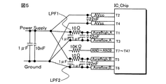
図5は、図1に示した本発明のひとつの実施形態に従った半導体集積回路を組み込んだマザーボードを示す回路図である。12ビットの局部D/A変換器12bit Local D/A_Convの主D/A変換器の255個の切り換えスイッチCSW0、CSW1…CSW254の一方の入力端子に共通接続された半導体集積回路の第1外部端子T1には、半導体集積回路外部からローパスフィルターLPF1を介してアナログ基準電圧AVrefhighが供給されている。このローパスフィルターLPF1は、10Ωの抵抗と、10Ωの抵抗の両端の1μFの容量、1μFと22nFとの並列容量とで構成されている。この12ビットの局部D/A変換器12bit Local D/A_Convの主D/A変換器の255個の切り換えスイッチCSW0、CSW1…CSW254の他方の入力端子に共通接続された半導体集積回路の第3外部端子T3には、半導体集積回路外部から基底電圧AVreflowが供給されている。副D/A変換器としての抵抗ストリング型D/A変換器の16個の抵抗R15、R14…R1、R0の直列接続の一端に接続された半導体集積回路の第2外部端子T2には、半導体集積回路外部からアナログ基準電圧AVccが供給されている。副D/A変換器としての抵抗ストリング型D/A変換器の16個の抵抗R15、R14…R1、R0の直列接続の他端に接続された半導体集積回路の第4外部端子T4には、半導体集積回路外部から基底電圧AVssが供給されている。尚、図5で、半導体集積回路の第5外部端子T5には、半導体集積回路外部からローパスフィルターLPF2を介してアナログ基準電圧AVrefhigh_Bが供給されている。半導体集積回路の第6外部端子T6には、半導体集積回路外部から基底電圧AVreflow_Bが供給されている。この半導体集積回路の第5外部端子T5と第6外部端子T6とには、別のチャンネルの12ビットの逐次比較型A/D変換器が接続されている。また、半導体集積回路の第7外部端子T7から第47外部端子T47には、10KΩのインピーダンスの各種のセンサーからのアナログセンス電圧が供給され、12ビットの逐次比較型A/D変換器12bit A/D_Convの電圧比較器Compのアナログ入力端子Analog_Inに供給されてA/D変換される。さらに、図5で、マザーボードシステムの統一電源電圧が1μFと10nFとの並列容量から供給されることによって、この統一電源電圧から複数の動作電源電圧が生成されている。 FIG. 5 is a circuit diagram showing a motherboard incorporating the semiconductor integrated circuit according to one embodiment of the present invention shown in FIG. First external terminal of a semiconductor integrated circuit commonly connected to one input terminal of 255 changeover switches CSW0, CSW1,..., CSW254 of a 12-bit local D / A converter 12bit Local D / A_Conv main D / A converter An analog reference voltage AVrefhigh is supplied to T1 from the outside of the semiconductor integrated circuit via a low-pass filter LPF1. The low-pass filter LPF1 is composed of a 10Ω resistor and a 1 μF capacitance at both ends of the 10Ω resistor, and a parallel capacitance of 1 μF and 22 nF. Third external circuit of the semiconductor integrated circuit commonly connected to the other input terminal of 255 change-over switches CSW0, CSW1,..., CSW254 of the main D / A converter of the 12-bit local D / A converter 12bit Local D / A_Conv. A base voltage AVreflow is supplied to the terminal T3 from the outside of the semiconductor integrated circuit. The second external terminal T2 of the semiconductor integrated circuit connected to one end of the series connection of 16 resistors R15, R14... R1, R0 of a resistor string type D / A converter as a sub D / A converter has a semiconductor An analog reference voltage AVcc is supplied from the outside of the integrated circuit. The fourth external terminal T4 of the semiconductor integrated circuit connected to the other end of the series connection of the 16 resistors R15, R14... R1, R0 of the resistor string type D / A converter as the sub D / A converter includes: A base voltage AVss is supplied from the outside of the semiconductor integrated circuit. In FIG. 5, the analog reference voltage AVrefhigh_B is supplied to the fifth external terminal T5 of the semiconductor integrated circuit from the outside of the semiconductor integrated circuit via the low pass filter LPF2. The base voltage AVreflow_B is supplied from the outside of the semiconductor integrated circuit to the sixth external terminal T6 of the semiconductor integrated circuit. A 12-bit successive approximation A / D converter of another channel is connected to the fifth external terminal T5 and the sixth external terminal T6 of this semiconductor integrated circuit. Analog sense voltages from various sensors having an impedance of 10 KΩ are supplied to the seventh external terminal T7 to the 47th external terminal T47 of the semiconductor integrated circuit, and a 12-bit successive approximation A / D converter 12bit A / The voltage is supplied to the analog input terminal Analog_In of the voltage comparator Comp of D_Conv and A / D converted. Further, in FIG. 5, a plurality of operating power supply voltages are generated from the unified power supply voltage by supplying the unified power supply voltage of the motherboard system from the parallel capacitance of 1 μF and 10 nF.
尚、図1に示し本発明のひとつの実施形態では、逐次比較型A/D変換器は、次のように動作するものとなる。12ビットの局部D/A変換器12bit Local D/A_Convの主D/A変換器としての容量アレー型D/A変換器は、その入力ダイナミックレンジの50%に対応する256個の切り換えスイッチCSW0、CSW1…CSW254、CSW255のうちの128個CSW0、CSW1…CSW127には第1外部端子T1のアナログ基準電圧AVrefhighが供給され、それ以外の切り換えスイッチCSW128…CSW254、CSW255には第3外部端子T3のアナログ基準電圧AVreflowが供給されている。この時のアナログ基準電圧Vxと入力アナログ信号Analog Inとが、電圧比較器Compで比較される。入力アナログ信号Analog Inがアナログ基準電圧Vxよりも高いと電圧比較器Compで判断されると、コントローラCntrlの出力に接続された8ビット入力デコーダ8bit_DECによって、12ビットの局部D/A変換器12bit Local D/A_Convの主D/A変換器としての容量アレー型D/A変換器の入力ダイナミックレンジの75%に対応する256個の切り換えスイッチCSW0、CSW1…CSW254、CSW255のうちの192個CSW0、CSW1…CSW191には第1外部端子T1のアナログ基準電圧AVrefhighが供給され、それ以外の切り換えスイッチCSW192…CSW254、CSW255には第3外部端子T3のアナログ基準電圧AVreflowが供給されている。逆に、力アナログ信号Analog Inが逐次基準電圧Vxよりも低いと電圧比較器Compで判断されると、コントローラCntrlの出力に接続された8ビット入力デコーダ8bit_DECによって、12ビットの局部D/A変換器12bit Local D/A_Convの主D/A変換器としての容量アレー型D/A変換器の入力ダイナミックレンジの25%に対応する256個の切り換えスイッチCSW0、CSW1…CSW254、CSW255のうちの64個のCSW0、CSW1…CSW63には第1外部端子T1のアナログ基準電圧AVrefhighが供給され、それ以外の切り換えスイッチCSW64…CSW254、CSW255には第3外部端子T3のアナログ基準電圧AVreflowが供給されている。 In one embodiment of the present invention shown in FIG. 1, the successive approximation type A / D converter operates as follows. The 12-bit local D / A converter 12-bit local D / A_Conv capacitive D / A converter as the main D / A converter has 256 switching switches CSW0 corresponding to 50% of its input dynamic range, The analog reference voltage AVrefhigh of the first external terminal T1 is supplied to 128 of the CSW1... CSW254, CSW255, CSW0, CSW1... CSW127, and the other changeover switches CSW128. A reference voltage AVreflow is supplied. At this time, the analog reference voltage Vx and the input analog signal Analog In are compared by the voltage comparator Comp. When the voltage comparator Comp determines that the input analog signal Analog In is higher than the analog reference voltage Vx, the 8-bit input decoder 8bit_DEC connected to the output of the controller Cntrl causes a 12-bit local D / A converter 12bit Local. 192 of CSW0, CSW1,..., CSW254, CSW255 corresponding to 75% of the input dynamic range of the capacitive array type D / A converter as the main D / A converter of D / A_Conv CSW0, CSW1 ... the analog reference voltage AVrefhigh of the first external terminal T1 is supplied to CSW191, and the analog reference voltage AVreflow of the third external terminal T3 is supplied to the other changeover switches CSW192 ... CSW254 and CSW255. . Conversely, when the voltage comparator Comp determines that the force analog signal Analog In is successively lower than the reference voltage Vx, a 12-bit local D / A conversion is performed by the 8-bit input decoder 8bit_DEC connected to the output of the controller Cntrl. 64 bits of 256 switches CSW0, CSW1,... CSW254, CSW255 corresponding to 25% of the input dynamic range of the capacitive array type D / A converter as the main D / A converter of the 12-bit Local D / A_Conv. The analog reference voltage AVrefhigh of the first external terminal T1 is supplied to CSW0, CSW1,... CSW63, and the analog reference voltage AVreflow of the third external terminal T3 is supplied to the other switches CSW64.
以上のようにして、逐次比較型A/D変換器では電圧比較器は入力アナログ信号と逐次基準電圧との比較を行い、その比較結果により逐次比較型A/D変換器のコントローラは逐次基準電圧を変更する。電圧比較器は、再度入力アナログ信号との比較を行い、またコントローラは逐次基準電圧を再度、変更すると言う逐次比較が実行される。比較結果による逐次基準電圧の変更に、局部D/A変換器が使用される。この逐次比較と逐次基準電圧の逐次の変更とにより、入力アナログ信号のレベルに応答して複数のビットの制御ディジタル信号が収束して、逐次比較型A/D変換が実行される。 As described above, in the successive approximation A / D converter, the voltage comparator compares the input analog signal with the successive reference voltage, and the controller of the successive approximation A / D converter determines the successive reference voltage according to the comparison result. To change. The voltage comparator again performs a comparison with the input analog signal, and the controller performs a successive comparison that sequentially changes the reference voltage again. A local D / A converter is used to change the successive reference voltage according to the comparison result. By the successive comparison and the successive change of the successive reference voltage, the control digital signal of a plurality of bits converges in response to the level of the input analog signal, and the successive approximation A / D conversion is executed.
図2は、本発明の他のひとつの実施形態によるチップ上に逐次比較型A/D変換器を含む半導体集積回路の構成を示す図である。 FIG. 2 is a diagram showing a configuration of a semiconductor integrated circuit including a successive approximation A / D converter on a chip according to another embodiment of the present invention.
同図の実施形態が図1に示した実施形態と相違するのは、下記の通りである。図2において、副D/A変換器としての抵抗ストリング型D/A変換器の複数の抵抗R15、R14…R1、R0の直列接続の一端は、第1のPチャンネルMOSトランジスタQp1のドレイン・ソース電流経路を介して半導体集積回路の第1外部端子T1に接続され、第2のPチャンネルMOSトランジスタQp2のドレイン・ソース電流経路を介して半導体集積回路の第2外部端子T2に接続され、副D/A変換器としての抵抗ストリング型D/A変換器の複数の抵抗R15、R14…R1、R0の直列接続の他端は、第1のNチャンネルMOSトランジスタQn1のドレイン・ソース電流経路を介して半導体集積回路の第3外部端子T3に接続され、第2のNチャンネルMOSトランジスタQn2のドレイン・ソース電流経路を介して半導体集積回路の第4外部端子T4に接続されていることである。第1のPチャンネルMOSトランジスタQp1のゲートはフリップフロップFF1の出力で制御され、第2のPチャンネルMOSトランジスタQp2のゲートはフリップフロップFF3の出力で制御され、第1のNチャンネルMOSトランジスタQn1のゲートはフリップフロップFF2の出力で制御され、第2のNチャンネルMOSトランジスタQn2のゲートはフリップフロップFF4の出力で制御される。 The embodiment shown in the figure is different from the embodiment shown in FIG. 1 as follows. In FIG. 2, one end of a series connection of a plurality of resistors R15, R14... R1, R0 of a resistor string type D / A converter as a sub D / A converter is the drain-source of the first P-channel MOS transistor Qp1. Connected to the first external terminal T1 of the semiconductor integrated circuit via the current path, connected to the second external terminal T2 of the semiconductor integrated circuit via the drain / source current path of the second P-channel MOS transistor Qp2, and connected to the sub-D The other end of the series connection of the resistors R15, R14... R1, R0 of the resistor string type D / A converter as the / A converter is connected via the drain / source current path of the first N-channel MOS transistor Qn1. Via the drain / source current path of the second N-channel MOS transistor Qn2 connected to the third external terminal T3 of the semiconductor integrated circuit Is that is connected to the fourth external terminal T4 of the conductor integrated circuits. The gate of the first P-channel MOS transistor Qp1 is controlled by the output of the flip-flop FF1, the gate of the second P-channel MOS transistor Qp2 is controlled by the output of the flip-flop FF3, and the gate of the first N-channel MOS transistor Qn1. Is controlled by the output of the flip-flop FF2, and the gate of the second N-channel MOS transistor Qn2 is controlled by the output of the flip-flop FF4.
これらフリップフロップFF1〜フリップフロップFF4の保持内容により、第1のPチャンネルMOSトランジスタQp1、第2のPチャンネルMOSトランジスタQp2、第1のNチャンネルMOSトランジスタQn1、第2のNチャンネルMOSトランジスタQn2の各トランジスタのオン・オフが制御される。これらフリップフロップFF1〜フリップフロップFF4の保持内容は、中央処理ユニットCPUによる制御プログラムにより設定可能である。中央処理ユニットCPUによる制御プログラムにより、第1のPチャンネルMOSトランジスタQp1をオフ状態、第2のPチャンネルMOSトランジスタQp2をオン状態、第1のNチャンネルMOSトランジスタQn1をオフ状態、第2のNチャンネルMOSトランジスタQn2をオン状態に制御することにより、図5に示したマザーボードの回路を実現することが可能となる。尚、第1のPチャンネルMOSトランジスタQp1、第2のPチャンネルMOSトランジスタQp2、第1のNチャンネルMOSトランジスタQn1、第2のNチャンネルMOSトランジスタQn2の各トランジスタのオン・オフ制御のための制御プログラムは、CPUバスCPU_Busに接続されたリードオンリーメモリROMまたはフラッシュ不揮発性メモリNV_Flashに格納されることができる。 Depending on the contents held by these flip-flops FF1 to FF4, each of the first P-channel MOS transistor Qp1, the second P-channel MOS transistor Qp2, the first N-channel MOS transistor Qn1, and the second N-channel MOS transistor Qn2 The on / off state of the transistor is controlled. The contents held in the flip-flops FF1 to FF4 can be set by a control program by the central processing unit CPU. According to a control program by the central processing unit CPU, the first P-channel MOS transistor Qp1 is turned off, the second P-channel MOS transistor Qp2 is turned on, the first N-channel MOS transistor Qn1 is turned off, and the second N-channel By controlling the MOS transistor Qn2 to be in the ON state, the circuit of the mother board shown in FIG. 5 can be realized. A control program for on / off control of each of the first P-channel MOS transistor Qp1, the second P-channel MOS transistor Qp2, the first N-channel MOS transistor Qn1, and the second N-channel MOS transistor Qn2. Can be stored in a read only memory ROM or a flash nonvolatile memory NV_Flash connected to the CPU bus CPU_Bus.
図3は、本発明の更に他のひとつの実施形態によるチップ上に逐次比較型A/D変換器を含む半導体集積回路の構成を示す図である。 FIG. 3 is a diagram showing a configuration of a semiconductor integrated circuit including a successive approximation A / D converter on a chip according to still another embodiment of the present invention.
同図の実施形態が図1に示した実施形態と相違するのは、下記の通りである。図3において、局部D/A変換器の主D/A変換器は容量アレー型D/A変換器で構成され、局部D/A変換器の副D/A変換器は抵抗ストリング型D/A変換器ではなく電流切り換え型D/A変換器で構成されている。この電流切り換え型D/A変換器は、電流値が1:2:3:4:5:6:7:8:9:10:11:12の比率で重み付けされた定電流源Io、2Io、…、16Ioと差動PチャンネルMOSトランジスタQp1,Qp2、Qp3、Qp4…Qp5、Qp6とから構成されている。この電流切り換え型D/A変換器も図1や図2の抵抗ストリング型D/A変換器と同様に、半導体集積回路外部のローパスフィルターLPF1の抵抗での電圧降下を発生する危険性がある。従って、電流切り換え型D/A変換器の定電流源Io、2Io、…、16Ioも半導体集積回路の第2外部端子T2に接続されている。 The embodiment shown in the figure is different from the embodiment shown in FIG. 1 as follows. In FIG. 3, the main D / A converter of the local D / A converter is composed of a capacitive array type D / A converter, and the sub D / A converter of the local D / A converter is a resistor string type D / A. It is composed of a current switching type D / A converter, not a converter. This current switching type D / A converter has constant current sources Io, 2Io whose current values are weighted at a ratio of 1: 2: 3: 4: 5: 6: 7: 8: 9: 10: 11: 12. .., 16Io and differential P-channel MOS transistors Qp1, Qp2, Qp3, Qp4... Qp5, Qp6. This current switching type D / A converter also has a risk of causing a voltage drop at the resistance of the low-pass filter LPF1 outside the semiconductor integrated circuit, like the resistor string type D / A converter of FIGS. Therefore, the constant current sources Io, 2Io,..., 16Io of the current switching type D / A converter are also connected to the second external terminal T2 of the semiconductor integrated circuit.
図4は、本発明の更に他のひとつの実施形態によるチップ上に逐次比較型A/D変換器を含む半導体集積回路の構成を示す図である。 FIG. 4 is a diagram showing a configuration of a semiconductor integrated circuit including a successive approximation A / D converter on a chip according to still another embodiment of the present invention.
同図の実施形態が図3に示した実施形態と相違するのは、電流切り換え型D/A変換器の定電流源Io、2Io、…、16Ioが第1のPチャンネルMOSトランジスタQp1のドレイン・ソース電流経路を介して半導体集積回路の第1外部端子T1に接続され、第2のPチャンネルMOSトランジスタQp2のドレイン・ソース電流経路を介して半導体集積回路の第2外部端子T2に接続されている。電流切り換え型D/A変換器の抵抗R0は、第1のNチャンネルMOSトランジスタQn1のドレイン・ソース電流経路を介して半導体集積回路の第3外部端子T3に接続され、第2のNチャンネルMOSトランジスタQn2のドレイン・ソース電流経路を介して半導体集積回路の第4外部端子T4に接続されていることである。第1のPチャンネルMOSトランジスタQp1のゲートはフリップフロップFF1の出力で制御され、第2のPチャンネルMOSトランジスタQp2のゲートはフリップフロップFF3の出力で制御され、第1のNチャンネルMOSトランジスタQn1のゲートはフリップフロップFF2の出力で制御され、第2のNチャンネルMOSトランジスタQn2のゲートはフリップフロップFF4の出力で制御される。 3 is different from the embodiment shown in FIG. 3 in that the constant current sources Io, 2Io,..., 16Io of the current switching type D / A converter are connected to the drains of the first P-channel MOS transistor Qp1. It is connected to the first external terminal T1 of the semiconductor integrated circuit via the source current path, and is connected to the second external terminal T2 of the semiconductor integrated circuit via the drain / source current path of the second P-channel MOS transistor Qp2. . The resistor R0 of the current switching type D / A converter is connected to the third external terminal T3 of the semiconductor integrated circuit via the drain / source current path of the first N-channel MOS transistor Qn1, and the second N-channel MOS transistor It is connected to the fourth external terminal T4 of the semiconductor integrated circuit via the drain / source current path of Qn2. The gate of the first P-channel MOS transistor Qp1 is controlled by the output of the flip-flop FF1, the gate of the second P-channel MOS transistor Qp2 is controlled by the output of the flip-flop FF3, and the gate of the first N-channel MOS transistor Qn1. Is controlled by the output of the flip-flop FF2, and the gate of the second N-channel MOS transistor Qn2 is controlled by the output of the flip-flop FF4.
これらフリップフロップFF1〜フリップフロップFF4の保持内容により、第1のPチャンネルMOSトランジスタQp1、第2のPチャンネルMOSトランジスタQp2、第1のNチャンネルMOSトランジスタQn1、第2のNチャンネルMOSトランジスタQn2の各トランジスタのオン・オフが制御される。これらフリップフロップFF1〜フリップフロップFF4の保持内容は、中央処理ユニットCPUによる制御プログラムにより設定可能である。中央処理ユニットCPUによる制御プログラムにより、第1のPチャンネルMOSトランジスタQp1をオフ状態、第2のPチャンネルMOSトランジスタQp2をオン状態、第1のNチャンネルMOSトランジスタQn1をオフ状態、第2のNチャンネルMOSトランジスタQn2をオン状態に制御することにより、図5に示したマザーボードの回路を実現することが可能となる。尚、第1のPチャンネルMOSトランジスタQp1、第2のPチャンネルMOSトランジスタQp2、第1のNチャンネルMOSトランジスタQn1、第2のNチャンネルMOSトランジスタQn2の各トランジスタのオン・オフ制御のための制御プログラムは、CPUバスCPU_Busに接続されたリードオンリーメモリROMまたはフラッシュ不揮発性メモリNV_Flashに格納されることができる。 Depending on the contents held by these flip-flops FF1 to FF4, each of the first P-channel MOS transistor Qp1, the second P-channel MOS transistor Qp2, the first N-channel MOS transistor Qn1, and the second N-channel MOS transistor Qn2 The on / off state of the transistor is controlled. The contents held in the flip-flops FF1 to FF4 can be set by a control program by the central processing unit CPU. According to a control program by the central processing unit CPU, the first P-channel MOS transistor Qp1 is turned off, the second P-channel MOS transistor Qp2 is turned on, the first N-channel MOS transistor Qn1 is turned off, and the second N-channel By controlling the MOS transistor Qn2 to be in the ON state, the circuit of the mother board shown in FIG. 5 can be realized. A control program for on / off control of each of the first P-channel MOS transistor Qp1, the second P-channel MOS transistor Qp2, the first N-channel MOS transistor Qn1, and the second N-channel MOS transistor Qn2. Can be stored in a read only memory ROM or a flash nonvolatile memory NV_Flash connected to the CPU bus CPU_Bus.
以上本発明者によってなされた発明を実施形態に基づいて具体的に説明したが、本発明はそれに限定されるものではなく、その要旨を逸脱しない範囲において種々変更可能であることは言うまでもない。 Although the invention made by the present inventor has been specifically described based on the embodiments, it is needless to say that the present invention is not limited thereto and can be variously modified without departing from the gist thereof.
例えば、本発明は、CPUを含むマイクロコントローラやマイクロプロセッサ以外にも各種の用途に使用されるシステムLSIやディジタル・アナログ・ミックスド・シグナルLSI等のように、制御プログラムで動作するコントローラと、容量アレー型の主DACと直流電流を流す副DACとからなる局部D/A変換器を含む逐次比較型A/D変換器とを具備するLSI全般に適用可能であることは言うまでもないであろう。 For example, the present invention includes a controller that operates according to a control program, such as a system LSI and a digital / analog mixed signal LSI used for various purposes in addition to a microcontroller including a CPU and a microprocessor, and a capacity. It goes without saying that the present invention can be applied to all LSIs including a successive approximation A / D converter including a local D / A converter including an array type main DAC and a sub DAC for passing a direct current.
IC Chip 半導体集積回路のチップ
Analog Cir アナログ回路ブロック
12bit A/D_Conv 12ビットの逐次比較型A/D変換器
12bit Local D/A_Conv 12ビットの局部D/A変換器
Comp 電圧比較器
Cntrl コントローラ
CO…C255、CSW0…CSW255 局部D/A変換器の主D/A変換器
RO…R15、RSW00…RSW15 局部D/A変換器の副D/A変換器
T1 第1外部端子
T2 第2外部端子
T3 第3外部端子
T4 第4外部端子
IC Chip Semiconductor Integrated Circuit Chip Analog Circuit Analog Circuit Block 12-bit A / D_Conv 12-bit Successive Approximation Type A / D Converter 12-bit Local D / A_Conv 12-Bit Local D / A Converter Comp Voltage Comparator Cntrl Controller CO ... C255 CSW0 ... CSW255 Main D / A converter RO ... R15, RSW00 ... RSW15 of the local D / A converter Sub D / A converter T1 of the local D / A converter T1 First external terminal T2 Second external terminal T3 Third External terminal T4 Fourth external terminal
Claims (20)
前記局部D/A変換器の主D/A変換器と副D/A変換器とは、それぞれ容量アレー型D/A変換器と抵抗ストリング型D/A変換器とで構成され、
前記主D/A変換器としての前記容量アレー型D/A変換器は、複数の容量と、前記複数の容量の一端に接続された複数の切り換えスイッチとにより構成され、前記複数の容量の他端は共通接続され共通接続の電圧は入力アナログ信号と比較される逐次基準電圧として電圧比較器に入力され、
前記複数の切り換えスイッチの各切り換えスイッチの一方の入力端子に半導体集積回路外部からローパスフィルターを介してアナログ基準電圧が共通に供給可能なように、前記複数の切り換えスイッチの各切り換えスイッチの前記一方の入力端子は半導体集積回路の第1外部端子に共通に接続され、
前記容量アレー型D/A変換器の前記複数の容量には1つの容量が追加され、この1つの追加容量の一端には下記の副D/A変換器からのLSB側逐次基準電圧が供給され、
前記局部D/A変換器の前記副D/A変換器としての前記抵抗ストリング型D/A変換器は、直列接続された複数の抵抗と、前記複数の抵抗の接続ノードに入力端子が接続された複数のスイッチとから構成され、
前記複数のスイッチの出力端子は共通接続されることによって、前記共通接続された複数のスイッチの前記出力端子から副D/A変換器からのLSB側逐次基準電圧が生成され、
前記副D/A変換器としての抵抗ストリング型D/A変換器の複数の抵抗の直列接続の一端には半導体集積回路外部から前記アナログ基準電圧が供給可能なように、前記複数の抵抗の前記直列接続の前記一端は半導体集積回路の第2外部端子に接続されている半導体集積回路。 Built-in successive approximation type A / D converter including local D / A converter,
The main D / A converter and the sub D / A converter of the local D / A converter are respectively composed of a capacitance array type D / A converter and a resistor string type D / A converter,
The capacitive array type D / A converter as the main D / A converter includes a plurality of capacitors and a plurality of changeover switches connected to one end of the plurality of capacitors. The end is connected in common and the voltage of the common connection is input to the voltage comparator as a sequential reference voltage compared with the input analog signal,
The one of the change-over switches of the plurality of change-over switches so that the analog reference voltage can be commonly supplied from the outside of the semiconductor integrated circuit to the one input terminal of each of the change-over switches via a low-pass filter. The input terminal is commonly connected to the first external terminal of the semiconductor integrated circuit,
One capacitor is added to the plurality of capacitors of the capacitor array type D / A converter, and an LSB side sequential reference voltage from the following sub D / A converter is supplied to one end of the one additional capacitor. ,
The resistor string type D / A converter as the sub D / A converter of the local D / A converter has a plurality of resistors connected in series and an input terminal connected to a connection node of the plurality of resistors. Consisting of multiple switches
By connecting the output terminals of the plurality of switches in common, the LSB side sequential reference voltage from the sub D / A converter is generated from the output terminals of the plurality of commonly connected switches,
One end of a plurality of resistors of a resistor string type D / A converter as the sub D / A converter is connected to one end of the plurality of resistors so that the analog reference voltage can be supplied from the outside of the semiconductor integrated circuit. The one end of the series connection is a semiconductor integrated circuit connected to a second external terminal of the semiconductor integrated circuit.
前記局部D/A変換器の主D/A変換器と副D/A変換器とは、それぞれ、容量アレー型D/A変換器と抵抗ストリング型D/A変換器とで構成され、
前記主D/A変換器としての前記容量アレー型D/A変換器は、複数の容量と、前記複数の容量の一端に接続された複数の切り換えスイッチとにより構成され、前記複数の容量の他端は共通接続され共通接続の電圧は入力アナログ信号と比較される逐次基準電圧として電圧比較器に入力され、
前記複数の切り換えスイッチの各切り換えスイッチの一方の入力端子に半導体集積回路外部からローパスフィルターを介してアナログ基準電圧が共通に供給可能なように、前記複数の切り換えスイッチの各切り換えスイッチの一方の入力端子は半導体集積回路の第1外部端子に共通に接続され、前記容量アレー型D/A変換器では、前記複数の容量に1つの容量が追加され、この1つの追加容量の一端には下記の副D/A変換器からのLSB側逐次基準電圧が供給され、
前記局部D/A変換器の前記副D/A変換器としての前記抵抗ストリング型D/A変換器は、直列接続された複数の抵抗と、前記複数の抵抗の接続ノードに入力端子が接続された複数のスイッチとから構成され、
前記複数のスイッチの出力端子は共通接続されることによって、共通接続された前記複数のスイッチの出力端子から前記副D/A変換器からのLSB側逐次基準電圧が生成され、前記副D/A変換器としての前記抵抗ストリング型D/A変換器の複数の抵抗の直列接続の一端には半導体集積回路外部から前記アナログ基準電圧が供給可能なように、前記複数の抵抗の前記直列接続の前記一端の接続先は前記第1外部端子から半導体集積回路の第2外部端子に切り替え可能とされている半導体集積回路。 Built-in successive approximation type A / D converter including local D / A converter,
The main D / A converter and the sub D / A converter of the local D / A converter are respectively composed of a capacitance array type D / A converter and a resistor string type D / A converter,
The capacitive array type D / A converter as the main D / A converter includes a plurality of capacitors and a plurality of changeover switches connected to one end of the plurality of capacitors. The end is connected in common and the voltage of the common connection is input to the voltage comparator as a sequential reference voltage compared with the input analog signal,
One input of each change-over switch of the plurality of change-over switches so that an analog reference voltage can be commonly supplied to the one input terminal of each change-over switch of the plurality of change-over switches from outside the semiconductor integrated circuit via a low-pass filter. The terminal is commonly connected to the first external terminal of the semiconductor integrated circuit. In the capacitor array type D / A converter, one capacitor is added to the plurality of capacitors, and one end of the one additional capacitor is The LSB side sequential reference voltage from the sub D / A converter is supplied,
The resistor string type D / A converter as the sub D / A converter of the local D / A converter has a plurality of resistors connected in series and an input terminal connected to a connection node of the plurality of resistors. Consisting of multiple switches
By connecting the output terminals of the plurality of switches in common, the LSB side sequential reference voltage from the sub D / A converter is generated from the output terminals of the plurality of switches connected in common, and the sub D / A The one end of the series connection of the plurality of resistors of the resistor string type D / A converter as the converter is supplied with the analog reference voltage from the outside of the semiconductor integrated circuit. A semiconductor integrated circuit in which one end can be switched from the first external terminal to the second external terminal of the semiconductor integrated circuit.
前記局部D/A変換器の主D/A変換器と副D/A変換器とは、それぞれ容量アレー型D/A変換器と電流切り換え型D/A変換器とで構成され、
前記主D/A変換器としての前記容量アレー型D/A変換器は、複数の容量と、前記複数の容量の一端に接続された複数の切り換えスイッチとにより構成され、前記複数の容量の他端は共通接続され共通接続の電圧は入力アナログ信号と比較される逐次基準電圧として電圧比較器に入力され、
前記複数の切り換えスイッチの各切り換えスイッチの一方の入力端子に半導体集積回路外部からローパスフィルターを介してアナログ基準電圧が共通に供給可能なように、前記複数の切り換えスイッチの各切り換えスイッチの前記一方の入力端子は半導体集積回路の第1外部端子に共通に接続され、
前記容量アレー型D/A変換器の前記複数の容量には1つの容量が追加され、この1つの追加容量の一端には下記の副D/A変換器からのLSB側逐次基準電圧が供給され、
前記局部D/A変換器の前記副D/A変換器としての前記電流切り換え型D/A変換器は、所定の比率で重み付けされた複数の定電流源と、この複数の定電流源にそれぞれ接続された複数の差動対トランジスタとから構成され、
前記複数の差動対トランジスタの一方の複数のトランジスタの出力端子は共通接続されることによって、前記共通接続された前記一方の複数のトランジスタの前記出力端子から副D/A変換器からのLSB側逐次基準電圧が生成され、
前記副D/A変換器としての前記電流切り換え型D/A変換器の前記複数の定電流源には半導体集積回路外部から前記アナログ基準電圧が供給可能なように、前記副D/A変換器としての前記電流切り換え型D/A変換器の前記複数の定電流源は半導体集積回路の第2外部端子に接続されている半導体集積回路。 Built-in successive approximation type A / D converter including local D / A converter,
The main D / A converter and the sub D / A converter of the local D / A converter are respectively composed of a capacitance array type D / A converter and a current switching type D / A converter,
The capacitive array type D / A converter as the main D / A converter includes a plurality of capacitors and a plurality of changeover switches connected to one end of the plurality of capacitors. The end is connected in common and the voltage of the common connection is input to the voltage comparator as a sequential reference voltage compared with the input analog signal,
The one of the change-over switches of the plurality of change-over switches so that the analog reference voltage can be commonly supplied from the outside of the semiconductor integrated circuit to the one input terminal of each of the change-over switches via a low-pass filter. The input terminal is commonly connected to the first external terminal of the semiconductor integrated circuit,
One capacitor is added to the plurality of capacitors of the capacitor array type D / A converter, and an LSB side sequential reference voltage from the following sub D / A converter is supplied to one end of the one additional capacitor. ,
The current switching type D / A converter as the sub D / A converter of the local D / A converter includes a plurality of constant current sources weighted at a predetermined ratio, and the plurality of constant current sources, respectively. A plurality of connected differential pair transistors,
By connecting the output terminals of one of the plurality of differential pair transistors in common, the LSB side from the sub D / A converter from the output terminal of the one of the plurality of commonly connected transistors A sequential reference voltage is generated,
The sub D / A converter is configured so that the analog reference voltage can be supplied to the plurality of constant current sources of the current switching type D / A converter as the sub D / A converter from the outside of the semiconductor integrated circuit. The plurality of constant current sources of the current switching type D / A converter are connected to a second external terminal of the semiconductor integrated circuit.
前記局部D/A変換器の主D/A変換器と副D/A変換器とは、それぞれ容量アレー型D/A変換器と電流切り換え型D/A変換器とで構成され、
前記主D/A変換器としての前記容量アレー型D/A変換器は、複数の容量と、前記複数の容量の一端に接続された複数の切り換えスイッチとにより構成され、前記複数の容量の他端は共通接続され共通接続の電圧は入力アナログ信号と比較される逐次基準電圧として電圧比較器に入力され、
前記複数の切り換えスイッチの各切り換えスイッチの一方の入力端子に半導体集積回路外部からローパスフィルターを介してアナログ基準電圧が共通に供給可能なように、前記複数の切り換えスイッチの各切り換えスイッチの一方の入力端子は半導体集積回路の第1外部端子に共通に接続され、
前記容量アレー型D/A変換器では、前記複数の容量に1つの容量が追加され、この1つの追加容量の一端には下記の副D/A変換器からのLSB側逐次基準電圧が供給され、
前記局部D/A変換器の前記副D/A変換器としての前記電流切り換え型D/A変換器は、所定の比率で重み付けされた複数の定電流源と、この複数の定電流源にそれぞれ接続された複数の差動対トランジスタとから構成され、
前記複数の差動対トランジスタの一方の複数のトランジスタの出力端子は共通接続されることによって、前記共通接続された前記一方の複数のトランジスタの前記出力端子から副D/A変換器からのLSB側逐次基準電圧が生成され、
前記副D/A変換器としての前記電流切り換え型D/A変換器の前記複数の定電流源には半導体集積回路外部から前記アナログ基準電圧が供給可能なように、前記副D/A変換器としての前記電流切り換え型D/A変換器の前記複数の定電流源の接続先が前記第1外部端子から半導体集積回路の第2外部端子に切り替え可能とされている半導体集積回路。 Built-in successive approximation type A / D converter including local D / A converter,
The main D / A converter and the sub D / A converter of the local D / A converter are respectively composed of a capacitance array type D / A converter and a current switching type D / A converter,
The capacitive array type D / A converter as the main D / A converter includes a plurality of capacitors and a plurality of changeover switches connected to one end of the plurality of capacitors. The end is connected in common and the voltage of the common connection is input to the voltage comparator as a sequential reference voltage compared with the input analog signal,
One input of each change-over switch of the plurality of change-over switches so that an analog reference voltage can be commonly supplied to the one input terminal of each change-over switch of the plurality of change-over switches from outside the semiconductor integrated circuit via a low-pass filter. The terminal is commonly connected to the first external terminal of the semiconductor integrated circuit,
In the capacitance array type D / A converter, one capacitor is added to the plurality of capacitors, and an LSB side sequential reference voltage from the following sub D / A converter is supplied to one end of the one additional capacitor. ,
The current switching type D / A converter as the sub D / A converter of the local D / A converter includes a plurality of constant current sources weighted at a predetermined ratio, and the plurality of constant current sources, respectively. A plurality of connected differential pair transistors,
By connecting the output terminals of one of the plurality of differential pair transistors in common, the LSB side from the sub D / A converter from the output terminal of the one of the plurality of commonly connected transistors A sequential reference voltage is generated,
The sub D / A converter is configured so that the analog reference voltage can be supplied to the plurality of constant current sources of the current switching type D / A converter as the sub D / A converter from the outside of the semiconductor integrated circuit. A semiconductor integrated circuit in which the connection destinations of the plurality of constant current sources of the current switching type D / A converter can be switched from the first external terminal to the second external terminal of the semiconductor integrated circuit.
Priority Applications (2)
| Application Number | Priority Date | Filing Date | Title |
|---|---|---|---|
| JP2006068758A JP4803729B2 (en) | 2006-03-14 | 2006-03-14 | Semiconductor integrated circuit |
| US11/657,485 US7391354B2 (en) | 2006-03-14 | 2007-01-25 | Semiconductor integrated circuit |
Applications Claiming Priority (1)
| Application Number | Priority Date | Filing Date | Title |
|---|---|---|---|
| JP2006068758A JP4803729B2 (en) | 2006-03-14 | 2006-03-14 | Semiconductor integrated circuit |
Publications (2)
| Publication Number | Publication Date |
|---|---|
| JP2007251323A JP2007251323A (en) | 2007-09-27 |
| JP4803729B2 true JP4803729B2 (en) | 2011-10-26 |
Family
ID=38517219
Family Applications (1)
| Application Number | Title | Priority Date | Filing Date |
|---|---|---|---|
| JP2006068758A Expired - Fee Related JP4803729B2 (en) | 2006-03-14 | 2006-03-14 | Semiconductor integrated circuit |
Country Status (2)
| Country | Link |
|---|---|
| US (1) | US7391354B2 (en) |
| JP (1) | JP4803729B2 (en) |
Family Cites Families (15)
| Publication number | Priority date | Publication date | Assignee | Title |
|---|---|---|---|---|
| JPH0622331B2 (en) * | 1984-04-06 | 1994-03-23 | 松下電器産業株式会社 | DA converter |
| JPH01296823A (en) * | 1988-05-25 | 1989-11-30 | Toshiba Corp | Analog-digital converter |
| JPH05175840A (en) * | 1991-12-24 | 1993-07-13 | Oki Electric Ind Co Ltd | Reference voltage supply circuit for a/d converter |
| US5675340A (en) * | 1995-04-07 | 1997-10-07 | Iowa State University Research Foundation, Inc. | Charge-redistribution analog-to-digital converter with reduced comparator-hysteresis effects |
| JP2814963B2 (en) * | 1995-08-14 | 1998-10-27 | 日本電気株式会社 | AD converter |
| US6144331A (en) * | 1998-04-08 | 2000-11-07 | Texas Instruments Incorporated | Analog to digital converter with a differential output resistor-digital-to-analog-converter for improved noise reduction |
| JP2000059220A (en) * | 1998-08-03 | 2000-02-25 | Mitsubishi Electric Corp | Analog-to-digital converter controlling method |
| JP3211793B2 (en) * | 1999-01-08 | 2001-09-25 | 日本電気株式会社 | AD converter |
| US6828927B1 (en) * | 2002-11-22 | 2004-12-07 | Analog Devices, Inc. | Successive approximation analog-to-digital converter with pre-loaded SAR registers |
| US6940445B2 (en) * | 2002-12-27 | 2005-09-06 | Analog Devices, Inc. | Programmable input range ADC |
| US6731232B1 (en) * | 2002-12-27 | 2004-05-04 | Analog Devices, Inc. | Programmable input range SAR ADC |
| JP2004260263A (en) * | 2003-02-24 | 2004-09-16 | Fujitsu Ltd | Ad converter |
| DE10314189B4 (en) * | 2003-03-28 | 2006-05-11 | Infineon Technologies Ag | Method and apparatus for calibrating a weighted network |
| US6844840B1 (en) * | 2003-10-14 | 2005-01-18 | Cirrus Logic, Inc. | Successive-approximation-register (SAR) analog-to-digital converter (ADC) and method utilizing N three-way elements |
| US7161512B1 (en) * | 2005-06-16 | 2007-01-09 | Qualcomm Inc. | Gain error correction in an analog-to-digital converter |
-
2006
- 2006-03-14 JP JP2006068758A patent/JP4803729B2/en not_active Expired - Fee Related
-
2007
- 2007-01-25 US US11/657,485 patent/US7391354B2/en not_active Expired - Fee Related
Also Published As
| Publication number | Publication date |
|---|---|
| JP2007251323A (en) | 2007-09-27 |
| US20070216558A1 (en) | 2007-09-20 |
| US7391354B2 (en) | 2008-06-24 |
Similar Documents
| Publication | Publication Date | Title |
|---|---|---|
| JP3229135B2 (en) | Analog / digital converter | |
| US20060232461A1 (en) | Successive approximation analog-to-digital converter with current steered digital-to-analog converter | |
| JP4741680B2 (en) | Flexible analog / digital converter | |
| JPH0125449B2 (en) | ||
| US8937568B2 (en) | D/A converter | |
| US6075477A (en) | Voltage selector for a D/A converter | |
| JP2005217870A (en) | A/d converter | |
| JP5477093B2 (en) | DA converter | |
| JP4803729B2 (en) | Semiconductor integrated circuit | |
| KR20020059803A (en) | Digital-to-analog converter | |
| US5065159A (en) | Digital to analog converter with switching logic minimization | |
| US5450023A (en) | Interface circuit using a limited number of pins in LSI applications | |
| JP2009123926A (en) | Reference voltage generating circuit, ad converter, da converter, and image processing apparatus | |
| JP2005268895A (en) | Switching circuit | |
| US6999016B2 (en) | D/A converter and semiconductor device | |
| JP2005295315A (en) | Successive comparison a/d converter and comparator | |
| US7403150B1 (en) | Analog-to-digital converter architecture using a capacitor array structure | |
| JP6785350B2 (en) | R-2R ladder resistance circuit, ladder resistance type D / A conversion circuit, and semiconductor device | |
| JP2008301287A (en) | D/a converter circuit and liquid crystal driving device | |
| JP2004260263A (en) | Ad converter | |
| KR0184151B1 (en) | A/d converter | |
| JP4439905B2 (en) | Variable attenuator circuit | |
| JP2007243656A (en) | A/d converter | |
| JPH04138725A (en) | D/a converter | |
| JP2010004422A (en) | D/a conversion circuit |
Legal Events
| Date | Code | Title | Description |
|---|---|---|---|
| A621 | Written request for application examination |
Free format text: JAPANESE INTERMEDIATE CODE: A621 Effective date: 20090226 |
|
| A711 | Notification of change in applicant |
Free format text: JAPANESE INTERMEDIATE CODE: A712 Effective date: 20100507 |
|
| A977 | Report on retrieval |
Free format text: JAPANESE INTERMEDIATE CODE: A971007 Effective date: 20110801 |
|
| TRDD | Decision of grant or rejection written | ||
| A01 | Written decision to grant a patent or to grant a registration (utility model) |
Free format text: JAPANESE INTERMEDIATE CODE: A01 Effective date: 20110804 |
|
| A01 | Written decision to grant a patent or to grant a registration (utility model) |
Free format text: JAPANESE INTERMEDIATE CODE: A01 |
|
| A61 | First payment of annual fees (during grant procedure) |
Free format text: JAPANESE INTERMEDIATE CODE: A61 Effective date: 20110805 |
|
| R150 | Certificate of patent or registration of utility model |
Free format text: JAPANESE INTERMEDIATE CODE: R150 |
|
| FPAY | Renewal fee payment (event date is renewal date of database) |
Free format text: PAYMENT UNTIL: 20140819 Year of fee payment: 3 |
|
| S531 | Written request for registration of change of domicile |
Free format text: JAPANESE INTERMEDIATE CODE: R313531 |
|
| R350 | Written notification of registration of transfer |
Free format text: JAPANESE INTERMEDIATE CODE: R350 |
|
| LAPS | Cancellation because of no payment of annual fees |