EP1579254B1 - Vertical taper waveguide - Google Patents
Vertical taper waveguide Download PDFInfo
- Publication number
- EP1579254B1 EP1579254B1 EP03796692A EP03796692A EP1579254B1 EP 1579254 B1 EP1579254 B1 EP 1579254B1 EP 03796692 A EP03796692 A EP 03796692A EP 03796692 A EP03796692 A EP 03796692A EP 1579254 B1 EP1579254 B1 EP 1579254B1
- Authority
- EP
- European Patent Office
- Prior art keywords
- segment
- thickness
- recited
- slab
- waveguides
- Prior art date
- Legal status (The legal status is an assumption and is not a legal conclusion. Google has not performed a legal analysis and makes no representation as to the accuracy of the status listed.)
- Expired - Lifetime
Links
- 238000003780 insertion Methods 0.000 claims abstract description 22
- 230000037431 insertion Effects 0.000 claims abstract description 22
- 230000007423 decrease Effects 0.000 claims abstract description 11
- 230000003287 optical effect Effects 0.000 claims abstract description 7
- 241000397426 Centroberyx lineatus Species 0.000 claims abstract description 5
- VYPSYNLAJGMNEJ-UHFFFAOYSA-N Silicium dioxide Chemical compound O=[Si]=O VYPSYNLAJGMNEJ-UHFFFAOYSA-N 0.000 claims description 10
- 238000000034 method Methods 0.000 claims description 9
- 239000000377 silicon dioxide Substances 0.000 claims description 5
- GPXJNWSHGFTCBW-UHFFFAOYSA-N Indium phosphide Chemical compound [In]#P GPXJNWSHGFTCBW-UHFFFAOYSA-N 0.000 claims description 3
- XUIMIQQOPSSXEZ-UHFFFAOYSA-N Silicon Chemical compound [Si] XUIMIQQOPSSXEZ-UHFFFAOYSA-N 0.000 claims description 3
- 150000001875 compounds Chemical class 0.000 claims description 3
- 239000012212 insulator Substances 0.000 claims description 3
- 239000004065 semiconductor Substances 0.000 claims description 3
- 229910052710 silicon Inorganic materials 0.000 claims description 3
- 239000010703 silicon Substances 0.000 claims description 3
- 230000003247 decreasing effect Effects 0.000 claims 1
- 238000007493 shaping process Methods 0.000 claims 1
- 230000000116 mitigating effect Effects 0.000 abstract 1
- 238000004519 manufacturing process Methods 0.000 description 6
- 229920002120 photoresistant polymer Polymers 0.000 description 5
- 230000008859 change Effects 0.000 description 4
- 239000000835 fiber Substances 0.000 description 3
- 230000007704 transition Effects 0.000 description 3
- 238000010586 diagram Methods 0.000 description 2
- 229910052732 germanium Inorganic materials 0.000 description 2
- GNPVGFCGXDBREM-UHFFFAOYSA-N germanium atom Chemical compound [Ge] GNPVGFCGXDBREM-UHFFFAOYSA-N 0.000 description 2
- 238000001020 plasma etching Methods 0.000 description 2
- 238000013459 approach Methods 0.000 description 1
- 230000008901 benefit Effects 0.000 description 1
- 238000005253 cladding Methods 0.000 description 1
- 230000008878 coupling Effects 0.000 description 1
- 238000010168 coupling process Methods 0.000 description 1
- 238000005859 coupling reaction Methods 0.000 description 1
- 238000005516 engineering process Methods 0.000 description 1
- 239000000463 material Substances 0.000 description 1
- 230000009466 transformation Effects 0.000 description 1
Images

Classifications
-
- G—PHYSICS
- G02—OPTICS
- G02B—OPTICAL ELEMENTS, SYSTEMS OR APPARATUS
- G02B6/00—Light guides; Structural details of arrangements comprising light guides and other optical elements, e.g. couplings
- G02B6/10—Light guides; Structural details of arrangements comprising light guides and other optical elements, e.g. couplings of the optical waveguide type
- G02B6/12—Light guides; Structural details of arrangements comprising light guides and other optical elements, e.g. couplings of the optical waveguide type of the integrated circuit kind
- G02B6/12007—Light guides; Structural details of arrangements comprising light guides and other optical elements, e.g. couplings of the optical waveguide type of the integrated circuit kind forming wavelength selective elements, e.g. multiplexer, demultiplexer
- G02B6/12009—Light guides; Structural details of arrangements comprising light guides and other optical elements, e.g. couplings of the optical waveguide type of the integrated circuit kind forming wavelength selective elements, e.g. multiplexer, demultiplexer comprising arrayed waveguide grating [AWG] devices, i.e. with a phased array of waveguides
- G02B6/12011—Light guides; Structural details of arrangements comprising light guides and other optical elements, e.g. couplings of the optical waveguide type of the integrated circuit kind forming wavelength selective elements, e.g. multiplexer, demultiplexer comprising arrayed waveguide grating [AWG] devices, i.e. with a phased array of waveguides characterised by the arrayed waveguides, e.g. comprising a filled groove in the array section
-
- G—PHYSICS
- G02—OPTICS
- G02B—OPTICAL ELEMENTS, SYSTEMS OR APPARATUS
- G02B6/00—Light guides; Structural details of arrangements comprising light guides and other optical elements, e.g. couplings
- G02B6/10—Light guides; Structural details of arrangements comprising light guides and other optical elements, e.g. couplings of the optical waveguide type
- G02B6/12—Light guides; Structural details of arrangements comprising light guides and other optical elements, e.g. couplings of the optical waveguide type of the integrated circuit kind
- G02B6/122—Basic optical elements, e.g. light-guiding paths
- G02B6/1228—Tapered waveguides, e.g. integrated spot-size transformers
Definitions
- An embodiment of the present invention is related to optical planar lightwave circuits and, more particularly, to a vertically tapered waveguide such as those between the waveguides at the slab-waveguide interface of an Arrayed Waveguide Grating (AWG) to mitigate insertion losses.
- AWG Arrayed Waveguide Grating
- Wavelength division multiplexing has transformed the single fiber into a high capacity information conduit.
- AWG Arrayed Waveguide Grating
- AWGs are extremely versatile devices that are capable of multiplexing or demultiplexing many different frequency channels simultaneously carried on a single fiber.
- AWG may perform many essential functions, such as optical crossconnect and optical add/drop multiplexing.
- optical crossconnect and optical add/drop multiplexing.
- AWG insertion loss is one of the key performance factors that determine the power budget in the system.
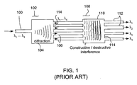
- Figure 1 illustrates an example of how a basic AWG may operate to demultiplex a plurality of channels.
- an AWG may comprise input / output waveguides, two slab regions and a phase array of planar waveguides which may have a constant path length difference with the neighboring waveguides.
- an input waveguide 100 simultaneously carries four multiplexed channels. Of course in practice, many times this number of channels are possible. Each channel is represented by a different wavelength or color of light denoted as ⁇ 1, ⁇ 2, ⁇ 3, and ⁇ 4.
- the light from the input waveguide 100 enters the first slab region 102.
- the input waveguide 100 is coupled at a first end 104 of the slab 102.
- the array of waveguides 106 fan out from the opposite side of the slab 102.
- Light input to the slab region 102 from the input waveguide 100 enters as a guided mode with confined mode dimension.
- the input waveguide - slab interface is designed to convert this guided mode in such a way that the wavefront will appear as a plane wave and conforms to the curvature of the output end of the slab 102.
- the output waveguides 106 capture the resultant light wave and carry it to a second slab region 108.
- Light carried in each output waveguides 106 is input to a second slab region 108.
- Each input carries a light signal containing components of ⁇ 1, ⁇ 2, ⁇ 3, and ⁇ 4, and again enters the second slab region 108 as guided mode.
- each of the output waveguides 112 of the second slab region 108 comprises only a single channel or wavelength.
- This arrangement works similarly in the reverse direction to multiplex a plurality of channels onto a single waveguide.
- Insertion loss typically occurs when a light signal travels or is inserted from one medium or waveguide to the next. At any transition point, some loss usually occurs. For example, reflection due to the difference in the index of refraction in the guiding media, scattering due to imperfection in the waveguide structure, diffraction due to abrupt change in the physical dimensions of the guiding media may contribute to loss. In the case of an AWG, one of the major contributions in the insertion loss occurs at the interface between the slab and the waveguides transition. For example, still referring to Figure 1 , the portion of the light signal that impinges the area between the waveguides 114 tends to be lost and contributes the overall insertion loss for the system.
- a portion of the AWG comprises a slab 200 and a plurality of waveguides 202-210.
- a vertically tapered waveguide 220 is formed between each waveguides 202-210 at the slab-waveguide interface.
- the vertically tapered waveguide 220 essentially comprises a wedge shaped portion having a vertical height matching the height of the slab 220 at the point 222 nearest the slab 200 which linearly decrease to a near zero height at its termination point 224 furthest from the slab 220.
- the shape of the waveguide 220 is also illustrated in Figure 2B which shows a vertical profile of the tapered waveguide 220 running alongside waveguide 210.
- the tapered waveguide 220 At its first end 222 nearest the slab 200, the tapered waveguide 220 has a height approximately the same as the height of the slab 200.
- the height of the waveguide linearly decreases to its terminal end 224 where, ideally, the height or thickness of the tapered waveguide 220 approaches a zero thickness.
- this is impossible given practical manufacturing constraints.
- Figure 2B when the thickness of the waveguide decreases to a height at or below current manufacturing capabilities, an uneven or jagged profile 226 results. These imperfections 226 cause scattering and contribute to insertion loss.
- FIG. 1 is a diagram illustrating multiplexing/demultiplexing operation of Arrayed Waveguide Gratings (AWGs);
- Figure 2A is a diagram illustrating an AWG including vertically tapered waveguides between the fingers to mitigate insertion loss
- Figure 2B is a side profile view of the of the AWG shown in Figure 2A ;
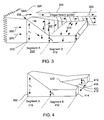
- Figure 3 is a plan view of a vertically tapered waveguide according to one embodiment of the invention.
- Figure 4 is a plan view of a vertically tapered waveguide according to another embodiment of the invention.
- Figure 5 is a plan view of a vertically tapered waveguide according to yet another embodiment of the invention.
- One of the embodiments of the invention comprises a vertically tapered waveguide such as to be used between the waveguides of an Arrayed Waveguide Grating (AWG).
- the waveguide does not require any special manufacturing tools or equipment and may be fabricated using traditional methods such as photoresist and reactive ion etching (RIE) techniques, for example.
- RIE reactive ion etching
- the film often breaks down beyond a certain minimum thickness.
- the breakup thickness for a particular photoresist may be around 0.3 ⁇ m. Below this minimum thickness, the photoresist in some cases is no longer a single, homogenous film with uniform thickness. Any breakage in the film may be transferred during fabrication and cause additional roughness on the etched surfaces such as that shown by 226 of Figure 2B .
- the photoresist needs to maintain a minimum thickness.
- FIG 3 there is shown a vertically tapered waveguide 300 according to one embodiment of the invention.
- the waveguide 300 has a horizontal profile 302 shaped to fit between the waveguides 304 and the slab 306 of an Arrayed Waveguide Grating (AWG).
- the vertical taper however, comprises two segments, denoted as Segment A 310, and Segment B 312.
- Segment A 310 has a vertical profile having a vertical taper that gradually or smoothly decreases from a first thickness or height h1, approximately equal to the height of the slab 306 to a second height h2.
- the second height h2 can be made as thin as current manufacturing technology can reliably resolve.
- a typical height for h1 and h2 may be around 6.0 ⁇ m and 2.0 ⁇ m, respectively.
- Segment B 312 has a substantially constant height equal to h2. Light, illustrated by the plurality of arrows 305, that enter the waveguide 300 tends to be channeled laterally into the adjacent fingers 304. This arrangement of leveling off the second segment 312 to a substantially constant height or thickness may avoid the terminal end imperfections (226 of Figure 2B ) and may improve insertion loss. Segment B 312, provides a smooth, gradual transition reducing scattering loss and thus further reducing insertion loss. Further, this design may reduce the aspect ratio for subsequent upper cladding disposition thus may reduce any gap fill problems.
- FIG. 4 shows yet another embodiment of the present invention similar to that shown in Figure 3 .
- Segment A 310 has a vertical taper wherein the thickness linearly decreases as the distance increases away from the slab 306 interface.
- Segment B 412 while still maintaining a substantially constant thickness h2, is forked and includes laterally tapered sidewalls 418 resulting in a swallowtail shape.
- the forked Segment B 412 may have two prongs 414 and 416.
- Each prong 414 and 416 has an inner sidewall 418 that is angled back into Segment B 412 to a triangular apex 422. This results in a wedged shaped cut out 420 formed along a central axis.
- Both prongs 414 and 416 have a substantially uniform or constant thickness equal to h2.
- This swallowtail shape may act to channel even more light entering the waveguide 300 laterally into the adjacent waveguides (304 of Figure 3 ) thus further reducing insertion loss.
- the vertical taper waveguide is about 180 ⁇ m in length. If this is used as a guideline, the length for Segment 310 in Fig. 4 may be about 120 ⁇ m since the minimum thickness for Segment 412 is about 2 ⁇ m. Assuming that the waveguides are separated by 30 ⁇ m and the minimum width at the tips of the two prongs, 414 and 416, are 2 ⁇ m. For this hypothetical example, the angle for the sidewall 418 may be about 25°.
- FIG. 5 shows additional embodiments of the invention.
- Segment B 512 is forked having a swallowtail shape.
- the forked Segment B 512 has two prongs 514 and 516.
- Each prong 514 and 516 has an inner sidewall 518 that is angled back into Segment B 412.
- the sidewalls 518 do not meet at a triangular apex, but rather each terminate at a flat vertical surface forming a flat apex 522.
- the point at which the sidewalls meet may form a rounded or may have a circular apex as illustrated by dashed line 524. Both of these variations may simplify manufacture since these shapes require less precision than the triangular apex 422 shown in Figure 4 .
- the disclosed waveguides can also be incorporated into many other optical devices. Indeed, any planar lightwave components with a Y-branch structure will benefit from using this tapered design.
- the vertical tapered waveguides can be employed to reduce the insertion loss of a Y-branch splitter.
- the disclosed waveguides can be manufactured from a variety of materials. Examples include silicon-on-insulator, silica, silicon oxynitride, indium phosphide, or any other compound semiconducting materials from Group III-V and II-VI.
Landscapes
- Physics & Mathematics (AREA)
- Engineering & Computer Science (AREA)
- Microelectronics & Electronic Packaging (AREA)
- General Physics & Mathematics (AREA)
- Optics & Photonics (AREA)
- Power Engineering (AREA)
- Optical Integrated Circuits (AREA)
- Optical Couplings Of Light Guides (AREA)
Applications Claiming Priority (3)
| Application Number | Priority Date | Filing Date | Title |
|---|---|---|---|
| US328478 | 1999-06-09 | ||
| US10/328,478 US6973236B2 (en) | 2002-12-24 | 2002-12-24 | Vertical taper waveguide |
| PCT/US2003/038694 WO2004061498A1 (en) | 2002-12-24 | 2003-12-05 | Vertical taper waveguide |
Publications (2)
| Publication Number | Publication Date |
|---|---|
| EP1579254A1 EP1579254A1 (en) | 2005-09-28 |
| EP1579254B1 true EP1579254B1 (en) | 2012-01-18 |
Family
ID=32594486
Family Applications (1)
| Application Number | Title | Priority Date | Filing Date |
|---|---|---|---|
| EP03796692A Expired - Lifetime EP1579254B1 (en) | 2002-12-24 | 2003-12-05 | Vertical taper waveguide |
Country Status (6)
| Country | Link |
|---|---|
| US (1) | US6973236B2 (enExample) |
| EP (1) | EP1579254B1 (enExample) |
| JP (1) | JP4904000B2 (enExample) |
| AT (1) | ATE542157T1 (enExample) |
| AU (1) | AU2003298930A1 (enExample) |
| WO (1) | WO2004061498A1 (enExample) |
Families Citing this family (12)
| Publication number | Priority date | Publication date | Assignee | Title |
|---|---|---|---|---|
| JP2003308714A (ja) * | 2002-04-17 | 2003-10-31 | Fuji Photo Film Co Ltd | 導光フィルム |
| US7245803B2 (en) * | 2003-02-11 | 2007-07-17 | Luxtera, Inc. | Optical waveguide grating coupler |
| US7006732B2 (en) * | 2003-03-21 | 2006-02-28 | Luxtera, Inc. | Polarization splitting grating couplers |
| US7773836B2 (en) | 2005-12-14 | 2010-08-10 | Luxtera, Inc. | Integrated transceiver with lightpipe coupler |
| JPWO2008066160A1 (ja) * | 2006-12-01 | 2010-03-11 | 日本電気株式会社 | 光変換器およびその製造方法 |
| US7862390B2 (en) * | 2007-05-16 | 2011-01-04 | Tyco Electronics Corporation | Power utility connector with a plurality of conductor receiving channels |
| US7974504B2 (en) * | 2008-03-28 | 2011-07-05 | Infinera Corporation | Reflection suppression in a photonic integrated circuit |
| US9335469B2 (en) * | 2012-01-31 | 2016-05-10 | Ignis Photonyx A/S | Planar optical branching circuit |
| US9164238B2 (en) | 2013-09-16 | 2015-10-20 | Electronics And Telecommunications Research Institute | Optical coupler having self-focusing region and arryed-waveguide grating structure including the same |
| JP6335676B2 (ja) * | 2014-06-19 | 2018-05-30 | 株式会社フジクラ | 基板型光導波路素子 |
| KR102364302B1 (ko) * | 2015-01-27 | 2022-02-21 | 한국전자통신연구원 | 평탄한 모드 발생 장치 및 이를 구비하는 배열 도파로 격자 |
| CA2994832C (en) * | 2015-08-05 | 2023-11-14 | Playhard, Inc. | Systems and methods for a stellate beam splitter |
Family Cites Families (18)
| Publication number | Priority date | Publication date | Assignee | Title |
|---|---|---|---|---|
| GB2227854B (en) | 1989-02-03 | 1993-05-12 | Stc Plc | Integrated optics asymmetric y-coupler |
| JPH08327836A (ja) * | 1995-05-29 | 1996-12-13 | Furukawa Electric Co Ltd:The | Y分岐光導波路回路 |
| JPH0961652A (ja) * | 1995-08-25 | 1997-03-07 | Nippon Telegr & Teleph Corp <Ntt> | 半導体光導波路およびその作製方法 |
| US6049644A (en) * | 1997-05-13 | 2000-04-11 | Lucent Technologies Inc. | Optical routing device having a substantially flat passband |
| US5889906A (en) | 1997-05-28 | 1999-03-30 | Lucent Technologies Inc. | Signal router with coupling of multiple waveguide modes for provicing a shaped multi-channel radiation pattern |
| US6069990A (en) * | 1997-11-27 | 2000-05-30 | Hitachi Cable Ltd. | Optical wavelength multiplexer/demultiplexer |
| DE69926844T2 (de) | 1998-09-03 | 2006-06-29 | Nippon Telegraph And Telephone Corp. | Planare Lichtwellenschaltung |
| JP2000147283A (ja) | 1998-09-03 | 2000-05-26 | Nippon Telegr & Teleph Corp <Ntt> | 光導波回路 |
| JP2000206352A (ja) * | 1999-01-14 | 2000-07-28 | Hitachi Cable Ltd | スポットサイズ変換コア構造を有する光導波路及びその製造方法 |
| JP2002107681A (ja) * | 2000-09-29 | 2002-04-10 | Fujitsu Quantum Devices Ltd | 光半導体装置 |
| JP2002228867A (ja) * | 2001-01-31 | 2002-08-14 | Fujikura Ltd | 光導波路の製造方法 |
| US6697552B2 (en) * | 2001-02-23 | 2004-02-24 | Lightwave Microsystems Corporation | Dendritic taper for an integrated optical wavelength router |
| JP3976514B2 (ja) * | 2001-04-05 | 2007-09-19 | 日本電気株式会社 | 光導波路の製造方法 |
| US20040114869A1 (en) * | 2001-06-15 | 2004-06-17 | Fike Eugene E. | Mode converter including tapered waveguide for optically coupling photonic devices |
| US20030032285A1 (en) * | 2001-08-13 | 2003-02-13 | Beguin Alain M.J. | Vertical taper fabrication process of a narrow band wavelength division multiplexer |
| US20030174956A1 (en) * | 2002-03-13 | 2003-09-18 | Jean-Francois Viens | Polarization insensitive modal field transformer for high index contrast waveguide devices |
| US6873766B2 (en) * | 2002-04-12 | 2005-03-29 | Corrado P. Dragone | Efficient waveguide arrays with nearly perfect element patterns |
| US6813432B2 (en) * | 2002-05-31 | 2004-11-02 | Intel Corporation | Method for producing vertical tapers in optical waveguides by over polishing |
-
2002
- 2002-12-24 US US10/328,478 patent/US6973236B2/en not_active Expired - Fee Related
-
2003
- 2003-12-05 WO PCT/US2003/038694 patent/WO2004061498A1/en not_active Ceased
- 2003-12-05 AU AU2003298930A patent/AU2003298930A1/en not_active Abandoned
- 2003-12-05 AT AT03796692T patent/ATE542157T1/de active
- 2003-12-05 EP EP03796692A patent/EP1579254B1/en not_active Expired - Lifetime
- 2003-12-05 JP JP2004565218A patent/JP4904000B2/ja not_active Expired - Fee Related
Also Published As
| Publication number | Publication date |
|---|---|
| AU2003298930A1 (en) | 2004-07-29 |
| EP1579254A1 (en) | 2005-09-28 |
| ATE542157T1 (de) | 2012-02-15 |
| US20040120674A1 (en) | 2004-06-24 |
| US6973236B2 (en) | 2005-12-06 |
| JP2006507542A (ja) | 2006-03-02 |
| WO2004061498A1 (en) | 2004-07-22 |
| JP4904000B2 (ja) | 2012-03-28 |
Similar Documents
| Publication | Publication Date | Title |
|---|---|---|
| US6580863B2 (en) | System and method for providing integrated optical waveguide device | |
| EP2329303B1 (en) | Method and apparatus for efficient coupling between silicon photonic chip and optical fiber | |
| EP2519846B1 (en) | Integrated optical receiver architecture for high speed optical i/o applications | |
| US7359593B2 (en) | Integrated optical mode shape transformer and method of fabrication | |
| US7668416B2 (en) | Single mode photonic circuit architecture and a new optical splitter design based on parallel waveguide mode conversion | |
| EP0856755B1 (en) | Optical waveguide coupler having low insertion loss | |
| US8254737B2 (en) | System and tapered waveguide for improving light coupling efficiency between optical fibers and integrated planar waveguides and method of manufacturing same | |
| US20060177180A1 (en) | Multichannel array waveguide diffraction grating multiplexer/demultiplexer and method of connecting array waveguide and output waveguide | |
| EP1579254B1 (en) | Vertical taper waveguide | |
| KR101121459B1 (ko) | 광섬유 및 평면 광학 도파관을 치밀하게 결합하는 방법 및장치 | |
| US7006744B2 (en) | Hybrid buried/ridge planar waveguides | |
| EP1462830A1 (en) | Optical waveguiding apparatus having reduced crossover losses | |
| US20020154849A1 (en) | Broadband wavelength-division multiplexer/demultiplexer | |
| CA2368945A1 (en) | Optical waveguide device having low insertion loss | |
| KR100417001B1 (ko) | 보조 광도파로를 구비한 광세기 분할기 | |
| US6741772B2 (en) | Optical multiplexer/demultiplexer and waveguide type optical coupler | |
| US6853792B2 (en) | Planar waveguide structure with segmented trenches and closely spaced, optically isolated waveguides | |
| US7085446B2 (en) | Optical multi/demultiplexer | |
| US6735363B1 (en) | Waveguide-grating router with output tapers configured to provide a passband that is optimized for each channel individually | |
| US11808996B1 (en) | Waveguides and edge couplers with multiple-thickness waveguide cores | |
| WO2002044772A1 (en) | Integrated optical waveguide device | |
| Itoh et al. | Ultra small 100 GHz 40 ch athermal AWG module using 2.5%-Δ silica-based waveguides | |
| US11536902B1 (en) | Edge couplers with metamaterial rib features | |
| EP1334385B1 (en) | Hybrid buried/ridge planar waveguides | |
| JP2005301301A (ja) | 光結合器 |
Legal Events
| Date | Code | Title | Description |
|---|---|---|---|
| PUAI | Public reference made under article 153(3) epc to a published international application that has entered the european phase |
Free format text: ORIGINAL CODE: 0009012 |
|
| 17P | Request for examination filed |
Effective date: 20050720 |
|
| AK | Designated contracting states |
Kind code of ref document: A1 Designated state(s): AT BE BG CH CY CZ DE DK EE ES FI FR GB GR HU IE IT LI LU MC NL PT RO SE SI SK TR |
|
| AX | Request for extension of the european patent |
Extension state: AL LT LV MK |
|
| DAX | Request for extension of the european patent (deleted) | ||
| 17Q | First examination report despatched |
Effective date: 20051221 |
|
| RIC1 | Information provided on ipc code assigned before grant |
Ipc: G02B 6/12 20060101AFI20110322BHEP |
|
| GRAP | Despatch of communication of intention to grant a patent |
Free format text: ORIGINAL CODE: EPIDOSNIGR1 |
|
| GRAS | Grant fee paid |
Free format text: ORIGINAL CODE: EPIDOSNIGR3 |
|
| GRAA | (expected) grant |
Free format text: ORIGINAL CODE: 0009210 |
|
| AK | Designated contracting states |
Kind code of ref document: B1 Designated state(s): AT BE BG CH CY CZ DE DK EE ES FI FR GB GR HU IE IT LI LU MC NL PT RO SE SI SK TR |
|
| REG | Reference to a national code |
Ref country code: GB Ref legal event code: FG4D |
|
| REG | Reference to a national code |
Ref country code: CH Ref legal event code: EP |
|
| REG | Reference to a national code |
Ref country code: AT Ref legal event code: REF Ref document number: 542157 Country of ref document: AT Kind code of ref document: T Effective date: 20120215 Ref country code: IE Ref legal event code: FG4D |
|
| REG | Reference to a national code |
Ref country code: DE Ref legal event code: R096 Ref document number: 60339787 Country of ref document: DE Effective date: 20120315 |
|
| REG | Reference to a national code |
Ref country code: NL Ref legal event code: VDEP Effective date: 20120118 |
|
| PG25 | Lapsed in a contracting state [announced via postgrant information from national office to epo] |
Ref country code: BE Free format text: LAPSE BECAUSE OF FAILURE TO SUBMIT A TRANSLATION OF THE DESCRIPTION OR TO PAY THE FEE WITHIN THE PRESCRIBED TIME-LIMIT Effective date: 20120118 Ref country code: NL Free format text: LAPSE BECAUSE OF FAILURE TO SUBMIT A TRANSLATION OF THE DESCRIPTION OR TO PAY THE FEE WITHIN THE PRESCRIBED TIME-LIMIT Effective date: 20120118 Ref country code: BG Free format text: LAPSE BECAUSE OF FAILURE TO SUBMIT A TRANSLATION OF THE DESCRIPTION OR TO PAY THE FEE WITHIN THE PRESCRIBED TIME-LIMIT Effective date: 20120418 |
|
| PG25 | Lapsed in a contracting state [announced via postgrant information from national office to epo] |
Ref country code: GR Free format text: LAPSE BECAUSE OF FAILURE TO SUBMIT A TRANSLATION OF THE DESCRIPTION OR TO PAY THE FEE WITHIN THE PRESCRIBED TIME-LIMIT Effective date: 20120419 Ref country code: PT Free format text: LAPSE BECAUSE OF FAILURE TO SUBMIT A TRANSLATION OF THE DESCRIPTION OR TO PAY THE FEE WITHIN THE PRESCRIBED TIME-LIMIT Effective date: 20120518 Ref country code: FI Free format text: LAPSE BECAUSE OF FAILURE TO SUBMIT A TRANSLATION OF THE DESCRIPTION OR TO PAY THE FEE WITHIN THE PRESCRIBED TIME-LIMIT Effective date: 20120118 |
|
| REG | Reference to a national code |
Ref country code: AT Ref legal event code: MK05 Ref document number: 542157 Country of ref document: AT Kind code of ref document: T Effective date: 20120118 |
|
| PG25 | Lapsed in a contracting state [announced via postgrant information from national office to epo] |
Ref country code: CY Free format text: LAPSE BECAUSE OF FAILURE TO SUBMIT A TRANSLATION OF THE DESCRIPTION OR TO PAY THE FEE WITHIN THE PRESCRIBED TIME-LIMIT Effective date: 20120118 |
|
| PG25 | Lapsed in a contracting state [announced via postgrant information from national office to epo] |
Ref country code: SI Free format text: LAPSE BECAUSE OF FAILURE TO SUBMIT A TRANSLATION OF THE DESCRIPTION OR TO PAY THE FEE WITHIN THE PRESCRIBED TIME-LIMIT Effective date: 20120118 Ref country code: DK Free format text: LAPSE BECAUSE OF FAILURE TO SUBMIT A TRANSLATION OF THE DESCRIPTION OR TO PAY THE FEE WITHIN THE PRESCRIBED TIME-LIMIT Effective date: 20120118 Ref country code: SE Free format text: LAPSE BECAUSE OF FAILURE TO SUBMIT A TRANSLATION OF THE DESCRIPTION OR TO PAY THE FEE WITHIN THE PRESCRIBED TIME-LIMIT Effective date: 20120118 Ref country code: RO Free format text: LAPSE BECAUSE OF FAILURE TO SUBMIT A TRANSLATION OF THE DESCRIPTION OR TO PAY THE FEE WITHIN THE PRESCRIBED TIME-LIMIT Effective date: 20120118 Ref country code: CZ Free format text: LAPSE BECAUSE OF FAILURE TO SUBMIT A TRANSLATION OF THE DESCRIPTION OR TO PAY THE FEE WITHIN THE PRESCRIBED TIME-LIMIT Effective date: 20120118 Ref country code: EE Free format text: LAPSE BECAUSE OF FAILURE TO SUBMIT A TRANSLATION OF THE DESCRIPTION OR TO PAY THE FEE WITHIN THE PRESCRIBED TIME-LIMIT Effective date: 20120118 |
|
| PLBE | No opposition filed within time limit |
Free format text: ORIGINAL CODE: 0009261 |
|
| STAA | Information on the status of an ep patent application or granted ep patent |
Free format text: STATUS: NO OPPOSITION FILED WITHIN TIME LIMIT |
|
| PG25 | Lapsed in a contracting state [announced via postgrant information from national office to epo] |
Ref country code: IT Free format text: LAPSE BECAUSE OF FAILURE TO SUBMIT A TRANSLATION OF THE DESCRIPTION OR TO PAY THE FEE WITHIN THE PRESCRIBED TIME-LIMIT Effective date: 20120118 Ref country code: SK Free format text: LAPSE BECAUSE OF FAILURE TO SUBMIT A TRANSLATION OF THE DESCRIPTION OR TO PAY THE FEE WITHIN THE PRESCRIBED TIME-LIMIT Effective date: 20120118 |
|
| 26N | No opposition filed |
Effective date: 20121019 |
|
| PG25 | Lapsed in a contracting state [announced via postgrant information from national office to epo] |
Ref country code: AT Free format text: LAPSE BECAUSE OF FAILURE TO SUBMIT A TRANSLATION OF THE DESCRIPTION OR TO PAY THE FEE WITHIN THE PRESCRIBED TIME-LIMIT Effective date: 20120118 |
|
| REG | Reference to a national code |
Ref country code: DE Ref legal event code: R097 Ref document number: 60339787 Country of ref document: DE Effective date: 20121019 |
|
| PG25 | Lapsed in a contracting state [announced via postgrant information from national office to epo] |
Ref country code: ES Free format text: LAPSE BECAUSE OF FAILURE TO SUBMIT A TRANSLATION OF THE DESCRIPTION OR TO PAY THE FEE WITHIN THE PRESCRIBED TIME-LIMIT Effective date: 20120429 |
|
| PG25 | Lapsed in a contracting state [announced via postgrant information from national office to epo] |
Ref country code: MC Free format text: LAPSE BECAUSE OF NON-PAYMENT OF DUE FEES Effective date: 20121231 |
|
| REG | Reference to a national code |
Ref country code: CH Ref legal event code: PL |
|
| REG | Reference to a national code |
Ref country code: IE Ref legal event code: MM4A |
|
| REG | Reference to a national code |
Ref country code: FR Ref legal event code: ST Effective date: 20130830 |
|
| PG25 | Lapsed in a contracting state [announced via postgrant information from national office to epo] |
Ref country code: IE Free format text: LAPSE BECAUSE OF NON-PAYMENT OF DUE FEES Effective date: 20121205 Ref country code: LI Free format text: LAPSE BECAUSE OF NON-PAYMENT OF DUE FEES Effective date: 20121231 Ref country code: CH Free format text: LAPSE BECAUSE OF NON-PAYMENT OF DUE FEES Effective date: 20121231 |
|
| PG25 | Lapsed in a contracting state [announced via postgrant information from national office to epo] |
Ref country code: FR Free format text: LAPSE BECAUSE OF NON-PAYMENT OF DUE FEES Effective date: 20130102 |
|
| PG25 | Lapsed in a contracting state [announced via postgrant information from national office to epo] |
Ref country code: TR Free format text: LAPSE BECAUSE OF FAILURE TO SUBMIT A TRANSLATION OF THE DESCRIPTION OR TO PAY THE FEE WITHIN THE PRESCRIBED TIME-LIMIT Effective date: 20120118 |
|
| PG25 | Lapsed in a contracting state [announced via postgrant information from national office to epo] |
Ref country code: LU Free format text: LAPSE BECAUSE OF NON-PAYMENT OF DUE FEES Effective date: 20121205 |
|
| PG25 | Lapsed in a contracting state [announced via postgrant information from national office to epo] |
Ref country code: HU Free format text: LAPSE BECAUSE OF FAILURE TO SUBMIT A TRANSLATION OF THE DESCRIPTION OR TO PAY THE FEE WITHIN THE PRESCRIBED TIME-LIMIT Effective date: 20031205 |
|
| PGFP | Annual fee paid to national office [announced via postgrant information from national office to epo] |
Ref country code: GB Payment date: 20180427 Year of fee payment: 15 |
|
| GBPC | Gb: european patent ceased through non-payment of renewal fee |
Effective date: 20181205 |
|
| PG25 | Lapsed in a contracting state [announced via postgrant information from national office to epo] |
Ref country code: GB Free format text: LAPSE BECAUSE OF NON-PAYMENT OF DUE FEES Effective date: 20181205 |
|
| PGFP | Annual fee paid to national office [announced via postgrant information from national office to epo] |
Ref country code: DE Payment date: 20200922 Year of fee payment: 18 |
|
| REG | Reference to a national code |
Ref country code: DE Ref legal event code: R119 Ref document number: 60339787 Country of ref document: DE |
|
| PG25 | Lapsed in a contracting state [announced via postgrant information from national office to epo] |
Ref country code: DE Free format text: LAPSE BECAUSE OF NON-PAYMENT OF DUE FEES Effective date: 20220701 |