EP1577689A1 - Stiftkopfbaugruppe - Google Patents
Stiftkopfbaugruppe Download PDFInfo
- Publication number
- EP1577689A1 EP1577689A1 EP05090054A EP05090054A EP1577689A1 EP 1577689 A1 EP1577689 A1 EP 1577689A1 EP 05090054 A EP05090054 A EP 05090054A EP 05090054 A EP05090054 A EP 05090054A EP 1577689 A1 EP1577689 A1 EP 1577689A1
- Authority
- EP
- European Patent Office
- Prior art keywords
- pins
- pin header
- frame
- row
- circuit board
- Prior art date
- Legal status (The legal status is an assumption and is not a legal conclusion. Google has not performed a legal analysis and makes no representation as to the accuracy of the status listed.)
- Withdrawn
Links
Images


Classifications
-
- H—ELECTRICITY
- H01—ELECTRIC ELEMENTS
- H01R—ELECTRICALLY-CONDUCTIVE CONNECTIONS; STRUCTURAL ASSOCIATIONS OF A PLURALITY OF MUTUALLY-INSULATED ELECTRICAL CONNECTING ELEMENTS; COUPLING DEVICES; CURRENT COLLECTORS
- H01R12/00—Structural associations of a plurality of mutually-insulated electrical connecting elements, specially adapted for printed circuits, e.g. printed circuit boards [PCB], flat or ribbon cables, or like generally planar structures, e.g. terminal strips, terminal blocks; Coupling devices specially adapted for printed circuits, flat or ribbon cables, or like generally planar structures; Terminals specially adapted for contact with, or insertion into, printed circuits, flat or ribbon cables, or like generally planar structures
- H01R12/50—Fixed connections
- H01R12/51—Fixed connections for rigid printed circuits or like structures
- H01R12/55—Fixed connections for rigid printed circuits or like structures characterised by the terminals
- H01R12/58—Fixed connections for rigid printed circuits or like structures characterised by the terminals terminals for insertion into holes
-
- H—ELECTRICITY
- H01—ELECTRIC ELEMENTS
- H01R—ELECTRICALLY-CONDUCTIVE CONNECTIONS; STRUCTURAL ASSOCIATIONS OF A PLURALITY OF MUTUALLY-INSULATED ELECTRICAL CONNECTING ELEMENTS; COUPLING DEVICES; CURRENT COLLECTORS
- H01R4/00—Electrically-conductive connections between two or more conductive members in direct contact, i.e. touching one another; Means for effecting or maintaining such contact; Electrically-conductive connections having two or more spaced connecting locations for conductors and using contact members penetrating insulation
- H01R4/02—Soldered or welded connections
- H01R4/028—Soldered or welded connections comprising means for preventing flowing or wicking of solder or flux in parts not desired
-
- H—ELECTRICITY
- H05—ELECTRIC TECHNIQUES NOT OTHERWISE PROVIDED FOR
- H05K—PRINTED CIRCUITS; CASINGS OR CONSTRUCTIONAL DETAILS OF ELECTRIC APPARATUS; MANUFACTURE OF ASSEMBLAGES OF ELECTRICAL COMPONENTS
- H05K2201/00—Indexing scheme relating to printed circuits covered by H05K1/00
- H05K2201/10—Details of components or other objects attached to or integrated in a printed circuit board
- H05K2201/10227—Other objects, e.g. metallic pieces
- H05K2201/10424—Frame holders
Definitions
- Fiber optic transceivers are used in a variety of applications, including storage area networks (SANs), local area networks (LANs), Fibre Channel, Gigabit Ethernet, and synchronous optical network (SONET) applications. Fiber optic transceivers can be used as the network interface in mainframe computers, workstations, servers, and storage devices. Fiber optic transceivers can also be used in a broad range of network devices, such as bridges, routers, hubs, and local and wide area switches.
- SANs storage area networks
- LANs local area networks
- SONET synchronous optical network
- the Cooperation Agreement specifies the package outline, circuit board layout, and pin function definitions for small form factor transceivers.
- One of the standard small form factor transceivers specified includes ten input/output (I/O) pins. Up to ten pins are mounted on one side of the transceiver package and up to ten pins are mounted on the opposite side of the transceiver package. The pins are secured to a printed circuit board (PCB) within the transceiver housing and extend through the transceiver housing for coupling to a host.
- PCB printed circuit board
- pins are manually soldered onto the printed circuit board for the I/O pins.
- the pins are typically edge clip pins or pin header assemblies soldered to the printed circuit board.
- the pins must be manually-aligned and the soldering process typically requires several steps.
- the manual soldering process adds to the cost of manufacturing of the transceivers.
- wicking between pins in the header may occur causing solder to flow between pins. This can result in a short between pins.
- the pin header for a transceiver comprises a frame comprising a rectangle that is indented on opposing sides of the rectangle, a first row of pins extending through the frame at a first angle to the rectangle, and a second row of pins extending through the frame at a second angle to the rectangle.
- the first row of pins is along a first side of the frame between the indented opposing sides and the second row of pins is along a second side of the frame between the indented opposing sides.
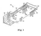
- FIG. 1 is a diagram illustrating one embodiment of a small form factor transceiver 30.
- Transceiver 30 is shown without a cover installed.
- Transceiver 30 includes housing 32, connector receptacle 36, printed circuit board (PCB) 34, and pin header 38.
- Pin header 38 includes ten pins 48 arranged into two rows of five pins each. In other embodiments, pin header 38 includes more than ten pins 48, such as fourteen pins in two rows of seven pins each. The two rows are situated on opposite sides of transceiver 30. One row of five pins is on one side of transceiver 30 and the other row of five pins is on the other side of transceiver 30.
- Housing 32 includes mounting studs 40 and 42 and apertures 44 and 46.
- Connector receptacle 36 and PCB 34 are coupled to housing 32.
- Pin header 38 is coupled (soldered) to PCB 34.
- Mounting studs 40 and 42 are situated on opposite sides of transceiver 30. Mounting stud 40 is on one side of transceiver 30 and mounting stud 42 is on the other side of transceiver 30. Mounting studs 40 and 42 are used to mount transceiver 30 to a host. Pins 48 of pin header 38 are used to pass signals between transceiver 30 and the host. One row of five pins 48 extends through aperture 44 of housing 32 and the other row of fives pins 48 extends through aperture 46 of housing 32. Both rows of five pins 48 couple to the host. Housing 32 is made of metal, plastic, or another suitable material. In one embodiment, transceiver 30, and spacing of pins 48, conforms to the industry standard small from factor transceiver specifications.
- FIG. 2 is a diagram illustrating a sectional view of one embodiment of pins 48 of pin header 38 extending through apertures 44 and 46 of housing 32 of transceiver 30.
- Transceiver 30 includes PCB 34, pin header 38, and housing 32.
- Pin header 38 includes frame 56 and pins 48.
- Pin header 38 is secured (soldered) to PCB 34 such that one row of five pins 48 extends through aperture 44 and the other row of five pins 48 extends through aperture 46.
- Frame 56 extends into aperture 44 to prevent the row of five pins 48 extending through aperture 44 from contacting housing 32.
- Frame 56 also extends into aperture 46 to prevent the other row of five pins 48 extending through aperture 46 from contacting housing 32.
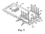
- FIG. 3 is a diagram illustrating one embodiment of PCB 34 of transceiver 30.
- PCB 34 includes pin header 38, test point 50, ten pre-plated through holes 52 that receive pins 48 of pin header 38, and transceiver components 53 and 54.
- Pin header 38 includes tens pins 48 and frame 56.
- Pins 48 are partially encased in frame 56 to maintain the alignment of pins 48.
- Frame 56 is rectangular with indented sides at 57a and 57b forming an hourglass shaped frame 56.
- Surface 56a of frame 56 is flat so pin header 38 can be handled by automated pick and place equipment.
- Automated pick and place equipment place pin header 38 on PCB 34 such that pins 48 are inserted into corresponding pre-plated through holes 52 of PCB 34.
- Pin header 38 is secured to PCB 34 by soldering pins 48 into the corresponding pre-plated through holes 52 of PCB 34.
- a solder reflow process is used to solder pins 48 into pre-plated through holes 52.
- Pogo-pin testing of PCB 34 can be performed after PCB 34 is installed in housing 32 as the hourglass shape of frame 56 allows a tester access to test point 50.
- the shape of frame 56 allows enough clearance such that components 54 can be mounted on PCB 34 underneath pin header 38.
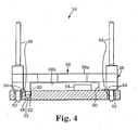
- Figure 4 is a diagram illustrating a side view of PCB 34 with mounted pin header 38.
- Pin header 38 includes pins 48, frame 56, standoffs 60, and alignment studs 62. Alignment studs 62 include conical tips 63.
- Component 54 can be mounted on PCB 34 underneath frame 56 of pin header 38. Pins 48 extend through pre-plated through holes 52 in PCB 34 and are soldered in pre-plated through holes 52. In one embodiment, pre-plated through holes 52 comprise copper.
- Standoffs 60 support pin header 38 on PCB 34. Standoffs 60 prevent solder from flowing between pins 48 in each row of pins during the soldering process by leaving enough space, indicated at 64, around each pin 48 to prevent wicking between pins 48.
- Alignment studs 62 (only one alignment stud is visible in Figure 4), are located on opposite corners of pin header 38 and extend parallel to pins 48. The alignment studs 62 are inserted into corresponding alignment stud holes 68 in PCB 34.
- Conical tips 63 of alignment studs 62 assist in the placement of pin header 38 on PCB 34 during manufacturing.
- Pick and place equipment place conical tips 63 into alignment stud holes 68 and release pin header 38.
- Pin header 38 falls into the correct position on PCB 34 as conical tips 63, and thus alignment studs 62 move to the center of alignment stud holes 68. This alignment process positions pins 48 in the desired location relative to PCB 34.
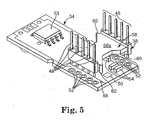
- Figure 5 is a diagram illustrating the placement of pin header 38 on PCB 34.
- PCB 34 includes the ten pre-plated through holes 52, components 53 and 54, test point 50, and alignment stud holes 68.
- Pin header 38 includes pins 48 and frame 56.
- Frame 56 includes standoffs 60 and alignment studs 62.
- One alignment stud 62 and the corresponding alignment stud hole 68 are located at the opposite corner of frame 56, indicated at 65, and are not visible in Figure 5.
- a pick and place tool automatically positions pin header 38 such that pins 48 are started in holes 52.
- Alignment studs 62 align themselves with the corresponding alignment stud holes 68 of PCB 34 as pin header 38 is lowered into place.
- the pins 48 are aligned with the corresponding pre-plated through holes 52 of PCB 34.
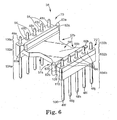
- Figure 6 is a diagram illustrating a perspective view of one embodiment of pin header 38.
- Pin header 38 includes the tens pins 48a - 48j captured in frame 56.
- Frame 56 includes standoffs 60a and 60b and alignment studs 62a and 62b.
- Alignment stud 62a includes conical tip 63a and alignment stud 62b includes conical tip 63b.
- Pins 48a - 48j are arranged in two rows 70 and 72 on opposite sides of frame 56.
- the first row 70 of five pins includes pins 48a - 48e and the second row 72 of five pins includes pins 48f - 48j.
- the center pin to center pin distance between the rows 70 and 72 of pins 48 is within the range of 9 mm to 11 mm, such as 10.16 mm per the Cooperation Agreement previously incorporated herein by reference.
- Pins 48a - 48j extend through frame 56 and include a shorter tail portion 100a and 100b extending up from frame 56, a captured portion 102a and 102b within frame 56, and a longer contact portion 104a and 104b extending down from frame 56.
- the tail portions 100a and 100b of pins 48a - 48j are configured for mounting in pre-plated through holes 52 of PCB 34.
- the captured portions 102a and 102b of pins 48a - 48j are enclosed within frame 56 to prevent movement of pins 48a - 48j.
- pins 48a - 48j can withstand (remain in frame 56) up to a nine pound pull out force.
- the contact portions 104a of pins 48a - 48e extend through aperture 46 of housing 32 and the contact portions 104b of pins 48f - 48j extend through aperture 44 of housing 32.
- Pins 48a - 48j are configured to electrically couple transceiver 30 to a host for transmitting signals between transceiver 30 and the host.
- pins 48a - 48j are round and made of copper or brass and are plated with gold for greater electrical conductivity.at solder joints and contacts. In one embodiment, the ends of pins 48a - 48j are not plated while the rest of the pin is plated. Pins 48a - 48j are rigid to resist bending and have a diameter within the range of 0.4 mm to 0.5 mm. The lengths of pins 48a - 48j are similar and within the range of 8 mm to 11 mm. Both ends of pins 48a - 48j are chamfered or rounded, such as at the ends 106 and 108 of pin 48f.
- Frame 56 includes standoffs 60a and 60b and alignment studs 62a and 62b.
- Standoffs 60a and 60b support pin header 38 on PCB 34 and form voids 64 between and around pins 48a - 48e and pins 48f - 48j, respectively.
- Voids 64 prevent solder from flowing between pins 48a - 48e and pins 48f - 48j to prevent wicking during the soldering of pin header 38 to PCB 34.
- Alignment stud 62a extends upward from the end of standoff 60a and alignment stud 62b extends upward from the end of standoff 60b.
- the conical tip 63a extends upward from alignment stud 62a and the conical tip 63b extends upward from alignment stud 62b.
- Conical tips 63a and 63b ease the alignment of alignment studs 62a and 62b into alignment stud holes 63 of PCB 34.
- Frame 56 is comprised of a liquid crystal polyiner that is injection molded around pins 48a - 48j.
- frame 56 is formed first and pins 48a - 48j are post inserted into frame 56.
- Frame 56 extends around pins 48a - 48j at captured portions 102a and 102b.
- frame 56 extends conically toward the ends of pins 48a - 48j, such as at 110 of pin 48f.
- conical portions, such as 110 are not included in frame 56.
- Frame 56 has a rectangular shape with indentations at 57a and 57b to form an hourglass shape.
- Frame 56 includes a flat surface 56b opposite surface 56a (not visible in Figure 6).
- frame 56 can withstand soldering temperatures up to 220 °C. In another embodiment, frame 56 can withstand soldering temperatures up to 300 °C.
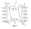
- FIG. 7 is a diagram illustrating a top view of one embodiment of pin header 38.
- Pin header 38 includes pins 48a - 48j and frame 56.
- Frame 56 includes standoffs 60a and 60b and alignment studs 62a and 62b.
- Frame 56 is rectangular with indented sides 57a and 57b to from an hourglass shape.
- One side 57b of the hourglass of frame 56 includes edges 200, 202, 204, and 206.
- the other side 57a of the hourglass of frame 56 includes edges 208, 210, 212, and 214.
- Edge 206 is perpendicular to standoff 60b and extends from standoff 60b to edge 204.
- Edges 204 and 200 angle inward toward the center 112 of frame 56 to edge 202.
- Edge 208 is perpendicular to standoff 60a and extends from standoff 60a to edge 210.
- Edges 210 and 214 angle inward toward the center 112 of frame 56 to edge 212.
- Alignment stud 62a is positioned at an end of standoff 60a and alignment stud 62b is positioned at an end of standoff 62b. Alignment studs 62a and 62b are positioned at opposite corners 216 and 218 of frame 56. Alignment studs 62a and 62b are circular in shape and standoffs 60a and 60b are rectangular in shape with rounded ends.
- Pin row 70 including pins 48a - 48e is parallel to pin row 72 including pins 48f-48j.
- Pin 48a is directly opposite pin 48f
- pin 48b is directly opposite pin 48g
- pin 48c is directly opposite pin 48h
- pin 48d is directly opposite pin 48i
- pin 48e is directly opposite pin 48j.
- Pins 48a - 48e of row 70 are equally spaced and pins 48f - 48j of row 72 are equally spaced.
- the center pin to center pin spacing between pins 48a - 48e and between pins 48f - 48j is within the range of 1 mm to 2 mm.
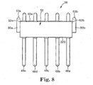
- Figure 8 is a diagram illustrating a side view of one embodiment of pin header 38.
- Pin header 38 includes pins 48a - 48e and frame 56.
- Frame 56 includes standoff 60a and alignment studs 62a and 62b.
- Alignment stud 62a includes conical tip 63a and alignment stud 62b includes conical tip 63b.
- Frame 56 also includes alignment stud bases 80a and 80b. Alignment stud bases 80a and 80b extend outwardly from frame 56 and are raised with respect to the bottom or one side, indicated at 220, of frame 56.
- Figure 9 is a diagram illustrating an end view of one embodiment of pin header 38.
- Pin header 38 includes pins 48a and 48f and frame 56.
- Frame 56 includes edges 208, 210, 212, and 214, conical portions 110 and 222, standoffs 60a and 60b, and alignment studs 62a and 62b.
- Alignment studs 62a includes conical tip 63a and alignment stud 62b includes conical tip 63b.
- Pin 48a includes tail portion 100a, captured portion 102a, and contact portion 104a.
- Pin 48f includes tail portion 100b, captured portion 102b, and contact portion 104b.
- conical portions, such as 110 extend from frame 56 toward pins 48 tail portions, such as 100a and 100b.
- Conical portions, such as 222 extend from frame 56 toward pins 48 contact portions, such as 104a and 104b.
- conical portions, such as 110 and 222 are not included in frame 56.
- Figure 10 is a diagram illustrating one pin 48f in frame 56 of pin header 38.
- Pin 48f includes the tail portion 100b, captured portion 102b, and contact portion 104b.
- the end 108 of tail portion 100b is chamfered or rounded and the end 106 of contact portion 104b is chamfered or rounded.
- the length of tail portion 100b is within the range of 1 mm to 2 mm.
- the length of captured portion 102b is within the range of 2 mm to 3 mm.
- the length of contact portion 104b is within the range of 4 mm to 6 mm.
- Frame 56 includes the center portion 112, a tail capture portion 224, and a contact capture portion 226.
- Tail capture portion 224 includes conical portion 110 extending from frame 56 toward the end 108 of tail portion 100b and contact capture portion 226 includes conical portion 222 extending from frame 56 toward the end 106 of contact portion 104b. In another embodiment, conical. portions 110 and 222 are not included in frame 56.
- Tail capture portion 224 extends above center portion 112 and contact capture portion 226 extends below center portion 112. In one embodiment, tail capture portion 224 is wider than contact capture portion 226.
- Tail capture portion 224 maintains a space between center portion 112 and PCB 34 to allow other components to be mounted on PCB 34 above center portion 112. With pin header 38 installed in housing 32, contact capture portion 226 and conical portion 222 prevent pin 48f from contacting housing 32 and causing a short. The other pins 48 in pin header 38 are similarly configured to pin 48f.
Landscapes
- Coupling Device And Connection With Printed Circuit (AREA)
Applications Claiming Priority (2)
| Application Number | Priority Date | Filing Date | Title |
|---|---|---|---|
| US804902 | 2004-03-19 | ||
| US10/804,902 US20050208797A1 (en) | 2004-03-19 | 2004-03-19 | Pin header |
Publications (1)
| Publication Number | Publication Date |
|---|---|
| EP1577689A1 true EP1577689A1 (de) | 2005-09-21 |
Family
ID=34838949
Family Applications (1)
| Application Number | Title | Priority Date | Filing Date |
|---|---|---|---|
| EP05090054A Withdrawn EP1577689A1 (de) | 2004-03-19 | 2005-03-07 | Stiftkopfbaugruppe |
Country Status (2)
| Country | Link |
|---|---|
| US (1) | US20050208797A1 (de) |
| EP (1) | EP1577689A1 (de) |
Cited By (2)
| Publication number | Priority date | Publication date | Assignee | Title |
|---|---|---|---|---|
| WO2014066805A1 (en) * | 2012-10-26 | 2014-05-01 | Continental Automotive Systems, Inc. | Pin header assembly and method of forming the same |
| US20170133725A1 (en) * | 2014-06-26 | 2017-05-11 | Robert Bosch Gmbh | Electrical connector for a battery module |
Families Citing this family (8)
| Publication number | Priority date | Publication date | Assignee | Title |
|---|---|---|---|---|
| JP2007194435A (ja) * | 2006-01-19 | 2007-08-02 | Fujitsu Ltd | 実装材整列基板、実装装置、実装方法及び回路基板製造方法 |
| JP2007194434A (ja) * | 2006-01-19 | 2007-08-02 | Fujitsu Ltd | 実装材整列基板、実装装置、実装方法及び回路基板製造方法 |
| US7744380B2 (en) * | 2007-02-21 | 2010-06-29 | Fci Americas Technology, Inc | Overmolded electrical contact array |
| US8145058B2 (en) * | 2007-08-13 | 2012-03-27 | Finisar Corporation, Inc. | Optical network unit transceiver module having direct connect RF pin configuration |
| JP5744092B2 (ja) * | 2013-03-22 | 2015-07-01 | 三菱電機株式会社 | 電子制御装置および電子制御装置の製造方法 |
| US9293848B2 (en) | 2014-05-29 | 2016-03-22 | Ideal Industries, Inc. | Electrical connector for use with printed circuit boards |
| JP6645413B2 (ja) * | 2016-12-15 | 2020-02-14 | 豊田合成株式会社 | 電子装置 |
| JP7541050B2 (ja) * | 2022-04-28 | 2024-08-27 | 矢崎総業株式会社 | 電子部品モジュール |
Citations (5)
| Publication number | Priority date | Publication date | Assignee | Title |
|---|---|---|---|---|
| US4627678A (en) * | 1983-01-24 | 1986-12-09 | Thomas & Betts Corporation | Electronic package assembly and accessory component therefor |
| US4655516A (en) * | 1984-12-20 | 1987-04-07 | Amp Incorporated | Chip carrier connector and method of making same |
| US5920461A (en) * | 1997-05-12 | 1999-07-06 | Lambda Electronics, Inc. | Surface mount power supply device |
| US20020126456A1 (en) * | 2001-02-28 | 2002-09-12 | Shunsuke Sato | Optical data link |
| US20030039454A1 (en) * | 2001-08-22 | 2003-02-27 | Gilliland Patrick B. | Dual channel device having two optical sub-assemblies |
Family Cites Families (13)
| Publication number | Priority date | Publication date | Assignee | Title |
|---|---|---|---|---|
| US4442938A (en) * | 1983-03-22 | 1984-04-17 | Advanced Interconnections | Socket terminal positioning method and construction |
| US4735587A (en) * | 1986-02-12 | 1988-04-05 | Specialty Electronics, Inc. | Pin header with board retention tail |
| US4695107A (en) * | 1986-06-09 | 1987-09-22 | Leppert James B | Integrated circuit sockets |
| JP3110494B2 (ja) * | 1991-06-14 | 2000-11-20 | バーグ・テクノロジー・インコーポレーテッド | コネクタ |
| US6402531B1 (en) * | 1998-10-05 | 2002-06-11 | Zierick Manufacturing Corp. | Capillary action enhanced surface mount pin header |
| US6461058B1 (en) * | 1999-10-28 | 2002-10-08 | Agilent Technologies, Inc. | Optoelectronic component |
| US6469906B1 (en) * | 2000-09-01 | 2002-10-22 | International Business Machines Corporation | Optical transceiver adaptation |
| US6371802B1 (en) * | 2000-11-21 | 2002-04-16 | Hon Hai Precision Ind. Co., Ltd. | Header connector with stabilizer |
| JP2002271074A (ja) * | 2001-03-08 | 2002-09-20 | Toshiba Corp | 冷却装置及び冷却装置を内蔵した電子機器 |
| US6575770B2 (en) * | 2001-08-01 | 2003-06-10 | Agilent Technologies, Inc. | Optoelectronic module apparatus and method of assembly |
| US6793533B2 (en) * | 2001-08-08 | 2004-09-21 | Molex Incorporated | Electrical connector assembly |
| US6589074B1 (en) * | 2002-07-31 | 2003-07-08 | Hon Hai Precision Ind. Co., Ltd. | Two ports integral electrical connector |
| US7130194B2 (en) * | 2002-10-31 | 2006-10-31 | Finisar Corporation | Multi-board optical transceiver |
-
2004
- 2004-03-19 US US10/804,902 patent/US20050208797A1/en not_active Abandoned
-
2005
- 2005-03-07 EP EP05090054A patent/EP1577689A1/de not_active Withdrawn
Patent Citations (5)
| Publication number | Priority date | Publication date | Assignee | Title |
|---|---|---|---|---|
| US4627678A (en) * | 1983-01-24 | 1986-12-09 | Thomas & Betts Corporation | Electronic package assembly and accessory component therefor |
| US4655516A (en) * | 1984-12-20 | 1987-04-07 | Amp Incorporated | Chip carrier connector and method of making same |
| US5920461A (en) * | 1997-05-12 | 1999-07-06 | Lambda Electronics, Inc. | Surface mount power supply device |
| US20020126456A1 (en) * | 2001-02-28 | 2002-09-12 | Shunsuke Sato | Optical data link |
| US20030039454A1 (en) * | 2001-08-22 | 2003-02-27 | Gilliland Patrick B. | Dual channel device having two optical sub-assemblies |
Cited By (4)
| Publication number | Priority date | Publication date | Assignee | Title |
|---|---|---|---|---|
| WO2014066805A1 (en) * | 2012-10-26 | 2014-05-01 | Continental Automotive Systems, Inc. | Pin header assembly and method of forming the same |
| US9153886B2 (en) | 2012-10-26 | 2015-10-06 | Continental Automotive Systems, Inc. | Pin header assembly and method of forming the same |
| US20170133725A1 (en) * | 2014-06-26 | 2017-05-11 | Robert Bosch Gmbh | Electrical connector for a battery module |
| US10978750B2 (en) * | 2014-06-26 | 2021-04-13 | Robert Bosch Gmbh | Electrical connector for a battery module |
Also Published As
| Publication number | Publication date |
|---|---|
| US20050208797A1 (en) | 2005-09-22 |
Similar Documents
| Publication | Publication Date | Title |
|---|---|---|
| US6227870B1 (en) | Connecting terminal and a connecting terminal assembly | |
| US5168432A (en) | Adapter for connection of an integrated circuit package to a circuit board | |
| US4550959A (en) | Surface mountable coefficient of expansion matching connector | |
| US5644839A (en) | Surface mountable substrate edge terminal | |
| US5184285A (en) | Socket constructed with molded-in lead frame providing means for installing additional component such as a chip capacitor | |
| US7179091B2 (en) | Edge mount electrical connector | |
| US5438481A (en) | Molded-in lead frames | |
| US20130078825A1 (en) | Method for connecting printed circuit boards | |
| US20090213563A1 (en) | Interconnecting device and method used to electrically mount a daughter board to a motherboard | |
| US11503732B1 (en) | Socket alignment and retention system | |
| EP1577689A1 (de) | Stiftkopfbaugruppe | |
| KR20230058734A (ko) | 컴퓨터 시스템 | |
| US6792675B2 (en) | Apparatus for aligning and soldering connectors to a printed board | |
| US6572389B2 (en) | Contact elements for surface mounting of burn-in socket | |
| EP3382811B1 (de) | Diskretes gerät | |
| US11735879B2 (en) | Adaptor for converting a ball grid array interface into a pin interface | |
| US6815614B1 (en) | Arrangement for co-planar vertical surface mounting of subassemblies on a mother board | |
| EP0125780A1 (de) | Auf der Leiterplattenoberfläche montierbarer, Wärmeausdehnungen ausgleichender Steckverbinder | |
| EP0767516A2 (de) | Bestückungsvorrichtung für elektrische Verbinder | |
| US20240170303A1 (en) | Interconnect alignment system and method | |
| KR101153164B1 (ko) | 고주파 커넥터용 접지 유니트 및 이를 갖는 고주파 커넥터 모듈 | |
| US10938136B2 (en) | Surface mounted card edge contact pair with pick-up carrier | |
| CN207396682U (zh) | 可靠性试验系统及其印刷电路板组件 | |
| KR102768587B1 (ko) | 커넥터 | |
| US7145085B2 (en) | Enhanced connection arrangement for co-planar vertical surface mounting of subassemblies on a mother board |
Legal Events
| Date | Code | Title | Description |
|---|---|---|---|
| PUAI | Public reference made under article 153(3) epc to a published international application that has entered the european phase |
Free format text: ORIGINAL CODE: 0009012 |
|
| AK | Designated contracting states |
Kind code of ref document: A1 Designated state(s): AT BE BG CH CY CZ DE DK EE ES FI FR GB GR HU IE IS IT LI LT LU MC NL PL PT RO SE SI SK TR |
|
| AX | Request for extension of the european patent |
Extension state: AL BA HR LV MK YU |
|
| AKX | Designation fees paid | ||
| STAA | Information on the status of an ep patent application or granted ep patent |
Free format text: STATUS: THE APPLICATION IS DEEMED TO BE WITHDRAWN |
|
| 18D | Application deemed to be withdrawn |
Effective date: 20060322 |
|
| REG | Reference to a national code |
Ref country code: DE Ref legal event code: 8566 |