US10938136B2 - Surface mounted card edge contact pair with pick-up carrier - Google Patents
Surface mounted card edge contact pair with pick-up carrier Download PDFInfo
- Publication number
- US10938136B2 US10938136B2 US16/411,393 US201916411393A US10938136B2 US 10938136 B2 US10938136 B2 US 10938136B2 US 201916411393 A US201916411393 A US 201916411393A US 10938136 B2 US10938136 B2 US 10938136B2
- Authority
- US
- United States
- Prior art keywords
- contact
- contact body
- circuit board
- card edge
- printed circuit
- Prior art date
- Legal status (The legal status is an assumption and is not a legal conclusion. Google has not performed a legal analysis and makes no representation as to the accuracy of the status listed.)
- Expired - Fee Related
Links
Images


Classifications
-
- H—ELECTRICITY
- H01—ELECTRIC ELEMENTS
- H01R—ELECTRICALLY-CONDUCTIVE CONNECTIONS; STRUCTURAL ASSOCIATIONS OF A PLURALITY OF MUTUALLY-INSULATED ELECTRICAL CONNECTING ELEMENTS; COUPLING DEVICES; CURRENT COLLECTORS
- H01R12/00—Structural associations of a plurality of mutually-insulated electrical connecting elements, specially adapted for printed circuits, e.g. printed circuit boards [PCB], flat or ribbon cables, or like generally planar structures, e.g. terminal strips, terminal blocks; Coupling devices specially adapted for printed circuits, flat or ribbon cables, or like generally planar structures; Terminals specially adapted for contact with, or insertion into, printed circuits, flat or ribbon cables, or like generally planar structures
- H01R12/70—Coupling devices
- H01R12/71—Coupling devices for rigid printing circuits or like structures
- H01R12/72—Coupling devices for rigid printing circuits or like structures coupling with the edge of the rigid printed circuits or like structures
- H01R12/722—Coupling devices for rigid printing circuits or like structures coupling with the edge of the rigid printed circuits or like structures coupling devices mounted on the edge of the printed circuits
-
- H—ELECTRICITY
- H01—ELECTRIC ELEMENTS
- H01R—ELECTRICALLY-CONDUCTIVE CONNECTIONS; STRUCTURAL ASSOCIATIONS OF A PLURALITY OF MUTUALLY-INSULATED ELECTRICAL CONNECTING ELEMENTS; COUPLING DEVICES; CURRENT COLLECTORS
- H01R12/00—Structural associations of a plurality of mutually-insulated electrical connecting elements, specially adapted for printed circuits, e.g. printed circuit boards [PCB], flat or ribbon cables, or like generally planar structures, e.g. terminal strips, terminal blocks; Coupling devices specially adapted for printed circuits, flat or ribbon cables, or like generally planar structures; Terminals specially adapted for contact with, or insertion into, printed circuits, flat or ribbon cables, or like generally planar structures
- H01R12/50—Fixed connections
- H01R12/51—Fixed connections for rigid printed circuits or like structures
- H01R12/55—Fixed connections for rigid printed circuits or like structures characterised by the terminals
- H01R12/57—Fixed connections for rigid printed circuits or like structures characterised by the terminals surface mounting terminals
-
- H—ELECTRICITY
- H01—ELECTRIC ELEMENTS
- H01R—ELECTRICALLY-CONDUCTIVE CONNECTIONS; STRUCTURAL ASSOCIATIONS OF A PLURALITY OF MUTUALLY-INSULATED ELECTRICAL CONNECTING ELEMENTS; COUPLING DEVICES; CURRENT COLLECTORS
- H01R13/00—Details of coupling devices of the kinds covered by groups H01R12/70 or H01R24/00 - H01R33/00
- H01R13/02—Contact members
- H01R13/22—Contacts for co-operating by abutting
- H01R13/24—Contacts for co-operating by abutting resilient; resiliently-mounted
- H01R13/2457—Contacts for co-operating by abutting resilient; resiliently-mounted consisting of at least two resilient arms contacting the same counterpart
-
- H—ELECTRICITY
- H01—ELECTRIC ELEMENTS
- H01R—ELECTRICALLY-CONDUCTIVE CONNECTIONS; STRUCTURAL ASSOCIATIONS OF A PLURALITY OF MUTUALLY-INSULATED ELECTRICAL CONNECTING ELEMENTS; COUPLING DEVICES; CURRENT COLLECTORS
- H01R43/00—Apparatus or processes specially adapted for manufacturing, assembling, maintaining, or repairing of line connectors or current collectors or for joining electric conductors
- H01R43/02—Apparatus or processes specially adapted for manufacturing, assembling, maintaining, or repairing of line connectors or current collectors or for joining electric conductors for soldered or welded connections
- H01R43/0256—Apparatus or processes specially adapted for manufacturing, assembling, maintaining, or repairing of line connectors or current collectors or for joining electric conductors for soldered or welded connections for soldering or welding connectors to a printed circuit board
-
- H—ELECTRICITY
- H01—ELECTRIC ELEMENTS
- H01R—ELECTRICALLY-CONDUCTIVE CONNECTIONS; STRUCTURAL ASSOCIATIONS OF A PLURALITY OF MUTUALLY-INSULATED ELECTRICAL CONNECTING ELEMENTS; COUPLING DEVICES; CURRENT COLLECTORS
- H01R43/00—Apparatus or processes specially adapted for manufacturing, assembling, maintaining, or repairing of line connectors or current collectors or for joining electric conductors
- H01R43/20—Apparatus or processes specially adapted for manufacturing, assembling, maintaining, or repairing of line connectors or current collectors or for joining electric conductors for assembling or disassembling contact members with insulating base, case or sleeve
- H01R43/205—Apparatus or processes specially adapted for manufacturing, assembling, maintaining, or repairing of line connectors or current collectors or for joining electric conductors for assembling or disassembling contact members with insulating base, case or sleeve with a panel or printed circuit board
-
- H—ELECTRICITY
- H01—ELECTRIC ELEMENTS
- H01R—ELECTRICALLY-CONDUCTIVE CONNECTIONS; STRUCTURAL ASSOCIATIONS OF A PLURALITY OF MUTUALLY-INSULATED ELECTRICAL CONNECTING ELEMENTS; COUPLING DEVICES; CURRENT COLLECTORS
- H01R12/00—Structural associations of a plurality of mutually-insulated electrical connecting elements, specially adapted for printed circuits, e.g. printed circuit boards [PCB], flat or ribbon cables, or like generally planar structures, e.g. terminal strips, terminal blocks; Coupling devices specially adapted for printed circuits, flat or ribbon cables, or like generally planar structures; Terminals specially adapted for contact with, or insertion into, printed circuits, flat or ribbon cables, or like generally planar structures
- H01R12/70—Coupling devices
- H01R12/71—Coupling devices for rigid printing circuits or like structures
- H01R12/712—Coupling devices for rigid printing circuits or like structures co-operating with the surface of the printed circuit or with a coupling device exclusively provided on the surface of the printed circuit
- H01R12/714—Coupling devices for rigid printing circuits or like structures co-operating with the surface of the printed circuit or with a coupling device exclusively provided on the surface of the printed circuit with contacts abutting directly the printed circuit; Button contacts therefore provided on the printed circuit
-
- H—ELECTRICITY
- H01—ELECTRIC ELEMENTS
- H01R—ELECTRICALLY-CONDUCTIVE CONNECTIONS; STRUCTURAL ASSOCIATIONS OF A PLURALITY OF MUTUALLY-INSULATED ELECTRICAL CONNECTING ELEMENTS; COUPLING DEVICES; CURRENT COLLECTORS
- H01R12/00—Structural associations of a plurality of mutually-insulated electrical connecting elements, specially adapted for printed circuits, e.g. printed circuit boards [PCB], flat or ribbon cables, or like generally planar structures, e.g. terminal strips, terminal blocks; Coupling devices specially adapted for printed circuits, flat or ribbon cables, or like generally planar structures; Terminals specially adapted for contact with, or insertion into, printed circuits, flat or ribbon cables, or like generally planar structures
- H01R12/70—Coupling devices
- H01R12/71—Coupling devices for rigid printing circuits or like structures
- H01R12/72—Coupling devices for rigid printing circuits or like structures coupling with the edge of the rigid printed circuits or like structures
- H01R12/722—Coupling devices for rigid printing circuits or like structures coupling with the edge of the rigid printed circuits or like structures coupling devices mounted on the edge of the printed circuits
- H01R12/728—Coupling devices without an insulating housing provided on the edge of the PCB
-
- H—ELECTRICITY
- H01—ELECTRIC ELEMENTS
- H01R—ELECTRICALLY-CONDUCTIVE CONNECTIONS; STRUCTURAL ASSOCIATIONS OF A PLURALITY OF MUTUALLY-INSULATED ELECTRICAL CONNECTING ELEMENTS; COUPLING DEVICES; CURRENT COLLECTORS
- H01R12/00—Structural associations of a plurality of mutually-insulated electrical connecting elements, specially adapted for printed circuits, e.g. printed circuit boards [PCB], flat or ribbon cables, or like generally planar structures, e.g. terminal strips, terminal blocks; Coupling devices specially adapted for printed circuits, flat or ribbon cables, or like generally planar structures; Terminals specially adapted for contact with, or insertion into, printed circuits, flat or ribbon cables, or like generally planar structures
- H01R12/70—Coupling devices
- H01R12/71—Coupling devices for rigid printing circuits or like structures
- H01R12/72—Coupling devices for rigid printing circuits or like structures coupling with the edge of the rigid printed circuits or like structures
- H01R12/73—Coupling devices for rigid printing circuits or like structures coupling with the edge of the rigid printed circuits or like structures connecting to other rigid printed circuits or like structures
- H01R12/735—Printed circuits including an angle between each other
- H01R12/737—Printed circuits being substantially perpendicular to each other
-
- H—ELECTRICITY
- H01—ELECTRIC ELEMENTS
- H01R—ELECTRICALLY-CONDUCTIVE CONNECTIONS; STRUCTURAL ASSOCIATIONS OF A PLURALITY OF MUTUALLY-INSULATED ELECTRICAL CONNECTING ELEMENTS; COUPLING DEVICES; CURRENT COLLECTORS
- H01R13/00—Details of coupling devices of the kinds covered by groups H01R12/70 or H01R24/00 - H01R33/00
- H01R13/02—Contact members
- H01R13/10—Sockets for co-operation with pins or blades
- H01R13/11—Resilient sockets
- H01R13/112—Resilient sockets forked sockets having two legs
-
- H—ELECTRICITY
- H01—ELECTRIC ELEMENTS
- H01R—ELECTRICALLY-CONDUCTIVE CONNECTIONS; STRUCTURAL ASSOCIATIONS OF A PLURALITY OF MUTUALLY-INSULATED ELECTRICAL CONNECTING ELEMENTS; COUPLING DEVICES; CURRENT COLLECTORS
- H01R2103/00—Two poles
Definitions
- the present application relates generally to field of electrical contacts, and more particularly to a type of electrical contact pair used to connect printed circuit boards (PCBs) in a perpendicular orientation.
- PCBs printed circuit boards
- connectors are used for forming electrical and mechanical connections between PCBs. These connectors can play a crucial role in achieving a design's size, cost, and performance constraints.
- Traditionally to connect two PCBs in a perpendicular orientation, a minimum of two electrical contacts are required. Affixing the electrical contacts to the PCB can be a difficult and inefficient process, as failure to hold a tight tolerance between the electrical contacts can result in suboptimal mating between the two PCBs.
- an efficient and reliable contact pair that can be precisely mounted on the edge of a PCB is needed.
- the systems, methods, and devices of this disclosure each have several innovative aspects, no single one of which is solely responsible for the desirable attributes disclosed herein.
- One embodiment of the invention relates to a card edge contact pair for electrically coupling printed circuit board assemblies.
- the card edge contact pair includes a first contact body and a second contact body.
- the first contact body includes a first solder joint end and a first deflection end.
- the second contact body includes a second solder joint end and a second deflection end.
- the card edge contact pair further includes an integral carrier component.
- the integral carrier component is detachably coupled to the first contact body and the second contact body.
- the first deflection end and the second deflection end are shaped using a forming process.
- the card edge contact pair includes a joint component that couples the first solder joint end and the second solder joint end to the integral carrier component.
- the joint component is configured to detachably couple from the first contact body and the second contact body.
- the card edge contact pair further includes a first score feature located at the intersection of the joint component and the first solder joint end, and a second score feature situated at the intersection of the joint component and the second solder joint end.
- the integral carrier component is oriented parallel to the first solder joint end and the second solder joint end.
- a system includes a first printed circuit board assembly and a second printed circuit board assembly.
- the first printed circuit board assembly includes a first printed circuit board and a first card edge contact pair coupled to the first printed circuit board.
- the first card edge contact pair includes a first contact body, a second contact body, and an integral carrier component detachably coupled to the first contact body and the second contact body.
- the second printed circuit board assembly is oriented perpendicularly with respect to the first printed circuit board assembly.
- the second printed circuit board assembly includes a second printed circuit board with a slot feature. A first contact surface and a second contact surface are located proximate to the slot feature. When the first printed board is inserted into the slot feature of the second printed circuit board, the first contact body is coupled to the first contact surface, and the second contact body is coupled to the second contact surface.
- the first contact body and the second contact body each include a solder joint end and a deflection end.
- the deflection ends are shaped using a forming process.
- the integral carrier component is oriented parallel to the solder joint ends.
- the first circuit board assembly includes a second card edge contact pair coupled to the first printed circuit board.
- the second card edge contact pair includes a third contact body and a fourth contact body.
- the second printed circuit board assembly includes a third contact surface and a fourth contact surface. The third contact body couples to the third contact surface and the fourth contact body couples to the fourth contact surface.
- Another embodiment of the invention relates to a method affixing a card edge contact pair to a printed circuit board assembly.
- the method includes removing a card edge contact pair from a packaging component.
- the card edge contact pair includes a first contact body and a second contact body detachably coupled to an integral carrier portion.
- the method further includes locating the card edge contact pair on a printed circuit board, fastening the card edge contact pair to the printed circuit board, and detaching the integral carrier portion from the first contact body and the second contact body.
- the first contact body and the second contact body each include a solder joint end and a deflection end.
- the deflection ends are shaped using a forming process.
- locating the card edge contact pair on the printed circuit board includes aligning the solder joint ends with solder pads located on the printed circuit board.
- the method is performed at least in part by automated component placement equipment.
- removing the card edge contact pair from the packaging component includes the automatic component placement equipment gripping the integral carrier portion by a vacuum device or a magnetic device.
- fastening the card edge contact pair to the printed circuit board includes a reflow solder process.
- the packaging component includes tape and reel packaging.
- FIG. 1 depicts an isometric view of a card edge contact pair in accordance with an illustrative embodiment.
- FIG. 2 depicts an isometric view of a card edge contact pair before engagement in accordance with an illustrative embodiment.
- FIG. 3 depicts an isometric view of a card edge contact pair after engagement in accordance with an illustrative embodiment.
- FIG. 4 depicts an isometric view of a dual card edge contact pair before engagement in accordance with an illustrative embodiment.
- FIG. 5 depicts an isometric view of a dual card edge contact pair after engagement in accordance with an illustrative embodiment.
- FIG. 6 depicts an isometric view of card edge contact pairs as shipped in accordance with an illustrative embodiment.
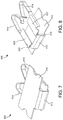
- FIG. 7 depicts an isometric view of a card edge contact pair as shipped in accordance with an illustrative embodiment.
- FIG. 8 depicts another isometric view of a card edge contact pair as shipped in accordance with an illustrative embodiment.
- FIG. 9 depicts an isometric view of a printed circuit board solder pad configuration in accordance with an illustrative embodiment.
- FIG. 10 depicts an isometric view of a mounted card edge contact pair as shipped in accordance with an illustrative embodiment.
- FIG. 11 depicts an isometric view of a card edge contact pair as shipped in accordance with another illustrative embodiment.
- FIG. 12 depicts a method of affixing a card edge contact pair to a PCB in accordance with an illustrative embodiment.
- a surface mounted card edge contact pair with an integral pick-up carrier may be used to mechanically and electrically couple two electrical current paths from a first printed circuit board (PCB) to a second PCB oriented in a direction perpendicular to the first PCB.
- PCB printed circuit board
- the inclusion of the integral pick-up carrier allows the two contacts to be precisely located relative to one another for optimal functioning.
- Existing card edge contact pair designs often utilize separately placed contacts, which may float relative to each other during a solder reflow process. If a tight tolerance is not enforced on the contact spacing, the result may be a sub-optimal contact gap and electrical connection.
- the mounted card edge contact pair assembly 100 includes a first contact body 102 and a second contact body 104 .
- the first contact body 102 and the second contact body 104 are symmetric.
- First contact body 102 is shown to terminate at a first solder joint end 106 and a first deflection end 110
- second contact body 104 is shown to terminate at a second solder joint end 108 and a second deflection end 112 .
- the solder joint ends 106 and 108 have a substantially rectangular shape and are oriented perpendicularly relative to the deflection ends 110 and 112 .
- the deflection ends 110 and 112 may be shaped to apply and maintain compression force between the contact bodies 102 and 104 and the contact surfaces of the mating PCB to maintain the required electrical connections. As depicted in FIG. 1 , deflection ends 110 and 112 may have a substantially hooked shape and may be bent backwards toward the solder joint ends 106 and 108 . In some embodiments, the deflection ends 110 and 112 are shaped using a forming process, as opposed to a stamping process. Use of a forming process can result in a smoother mating interface surface than the mating interface surface provided by an edge-blanked contact.
- the first contact body 102 and the second contact body 104 are shown to be mounted on a PCB 114 through a first solder pad 116 and a second solder pad 118 .
- the PCB 114 may be fabricated from any suitable material (e.g., FR4) and may be any required number of layers. In an illustrative embodiment, PCB 114 is smaller than the mating PCB (described in further detail below with respect to FIGS. 2 and 3 ).
- the first solder pad 116 and the second solder pad 118 may have a substantially rectangular shape and may be formed using a layer of solder paste.
- the solder paste may be a mixture of powdered solder and flux that is configured to melt under a controlled heating process to permanently join the first contact body 102 and the second contact body 104 to the PCB 114 . Further details regarding an illustrative embodiment of the PCB and solder pad geometry is included below with reference to FIG. 9 .
- First contact body 102 and second contact body 104 may be fabricated from any suitable conductive material, in any dimensions required to withstand the deflection forces generated as the contact pair assembly 100 is mated with a corresponding PCB assembly.
- the first contact body 102 and the second contact body 104 are fabricated from gold-plated beryllium copper (BeCu). BeCu may be selected for its high deflection range and good fatigue resistance, while gold plating may enhance the conduction capabilities of the first contact body 102 and the second contact body 104 .
- Gold plating is non-reactive as compared with other most other metals, and does not oxidize or rust in the presence of moisture and heat.
- Mating PCB assembly 200 is shown to include, among other components, a PCB 202 with a first contact surface 204 and a second contact surface 206 .
- the contact surfaces 204 and 206 abut a slot feature 208 .
- the width of the slot feature 208 may be selected such that the PCB 114 is able to be easily inserted into the slot feature 208 .
- the slot feature 208 is located proximate to one or more beveled or chamfered surfaces 210 .
- the chamfered surfaces 210 eliminate sharp corners surrounding the slot feature 208 and may increase the ease of mating the mounted card edge contact pair assembly 100 with the mating PCB assembly 200 .
- the depth that the slot feature 208 extends into the PCB 202 may be selected such that the deflection ends 110 and 112 of the contact pair assembly 100 make full contact with the contact surfaces 204 and 206 . As the deflection ends 110 and 112 slide over the contact surfaces 204 and 206 , the deflection ends 110 and 112 deflect away from the center of the contact pair assembly 100 .
- the first contact surface 204 and the second contact surface 206 may be fabricated from any suitable conductive material. For example, in some embodiments, the first and second contact surfaces 204 and 206 are gold plated.
- dual-mounted card edge contact pair assembly 300 is shown prior and subsequent to engagement with a mating PCB assembly 400 . Similar to the contact pair assembly 100 described above, dual-mounted card edge contact pair assembly 300 is shown to include a first contact body 302 with a first deflection end 312 and a second contact body 304 with a second deflection end 314 . The first contact body 302 and the second contact body 304 are shown to be surface mounted to PCB 316 . Dual-mounted card edge contact pair assembly 300 is further shown to include a third contact body 308 and a fourth contact body 310 , thereby increasing the number of potential electrical connections between assemblies 300 and 400 from two to four.
- Mating PCB assembly 400 is shown to include a PCB 402 with a first contact surface 404 and a second contact surface 406 situated above and below a slot feature 408 (third and fourth contact surfaces, not shown, may be located on the opposite side of PCB 402 ).
- contact surfaces 404 and 406 are identical or substantially similar to contact surfaces 204 and 206 , described above with reference to FIGS. 2-3 .
- Mating PCB assembly 400 may also include multiple chamfered surfaces 410 and 412 proximate to the slot feature 408 . Chamfered surfaces 410 and 412 may aid in the alignment and insertion of dual-mounted card edge contact pair assembly 300 into the slot feature 408 mating PCB assembly 400 .
- shipping assembly 600 is shown to comprise tape and reel packaging with embossed carrier tape segments 602 sealed by a cover tape 604 .
- Tape and reel packaging is utilized with automated placement equipment, also known as “pick-and-place” equipment, that is capable of placing thousands of surface mount components on a PCB per hour.
- each carrier tape segment 602 is shown to include multiple sprocket holes 603 that are utilized by a feeder component of an automated placement machine to advance the carrier tape segments 602 into the machine.
- cover tape 604 may be selected such that cover tape 604 remains adhered to carrier tape segments 602 under normal handling, while at the same time being removable by the automated placement equipment.
- Each embossed carrier tape segment 602 is shown to include a pocket 606 that partially encapsulates a card edge contact pair in its shipping configuration 608 .
- the size of pocket 606 may be chosen such that the contact bodies of contact pair 608 are prevented from excessive movement and damage during handling and storage procedures.
- the contact pair 608 includes an integral carrier portion 610 connected to a first contact body 614 and a second contact body 616 by a carrier joint 612 .
- the integral carrier portion 610 may be utilized to remove the contact pair 608 from packaging materials and to maintain a desired spacing between the first contact body 614 and the second contact body 616 during a process of affixing the contact pair 608 to a PCB.
- the integral carrier portion 610 and the carrier joint 612 are fabricated from the same material or materials as the first contact body 614 and the second contact body 616 .
- the integral carrier portion 610 may have a substantially rectangular shape and may be oriented parallel to the solder joint ends 622 and 624 of the contact bodies 614 and 616 .
- integral carrier portion 610 may have any desired shape that permits the gripping mechanism of the automatic placement equipment (e.g., a vacuum gripping mechanism, a multi-finger gripping mechanism, a magnetic gripping mechanism) to remove the contact pair 608 from the packaging materials.
- the gripping mechanism of the automatic placement equipment e.g., a vacuum gripping mechanism, a multi-finger gripping mechanism, a magnetic gripping mechanism
- Card edge contact pair 608 is further shown to include a first score feature 618 situated between the intersection of the first contact body 614 and the carrier joint 612 , and a second score feature 620 situated between the intersection of the second contact body 616 and the carrier joint 612 .
- First score feature 618 and second score feature 620 may increase the ease of detaching the integral carrier portion 610 and the carrier joint 612 from the contact bodies 614 and 616 by providing clean lines along which the carrier joint 612 can be detached from the contact bodies 614 and 616 .
- integral carrier portion 610 and carrier joint 612 may be detached from contact bodies 614 and 616 via any suitable manual or automatic process.
- detaching the integral carrier portion 610 and carrier joint 612 may comprise rotating the integral carrier portion 610 relative to the contact bodies 614 and 616 until the integral carrier portion 610 and carrier joint 612 snap free of the contact bodies 614 and 616 along the first score feature 618 and the second score feature 620 .
- PCB 902 is identical or substantially similar to PCB 114
- solder pads 904 and 906 are identical or substantially similar to solder pads 116 and 118 , each of which is described above with reference to FIG. 1
- PCB assembly 900 is further shown to include a first chamfered surface 908 and a second chamfered surface 910 proximate to a notch feature 912 .
- Notch feature 912 may aid in aligning the PCB assembly 900 with a slot feature in a mating PCB assembly.
- the first contact body 614 may be coupled to the solder pad 904
- the second contact body 616 may be coupled to the solder pad 906
- Integral carrier portion 610 may be situated above the contact bodies 614 and 616 in preparation for a detachment process.
- contact pair 1100 is shown to include a first contact body 1102 that terminates in a first solder joint end 1106 and a first deflection end 1110 , and a second contact body 1104 that terminates in a second solder joint end 1108 and a second deflection end 1112 .
- contact pair 1100 is shown to include an integral carrier portion 1114 extending from and connecting the first contact body 1102 to the second contact body 1104 in the same plane as the first solder joint end 1106 and the second solder joint end 1108 .
- contact pair 1100 may be preferred where PCB space permits, as the stamping process required to fabricate contact pair 1100 is simpler than the stamping process required to fabricate contact pair 608 .
- the integral carrier portion 1114 may be detached from the first contact body 1102 and the second contact body 1104 once the contact bodies 1102 and 1104 are affixed to the PCB.
- the first contact body 1102 and the second contact body 1104 are electrically common, and the integral carrier portion 1114 may remain permanently coupled to the first contact body 1102 and the second contact body 1104 .
- FIG. 12 depicts a method 1200 of affixing a card edge contact pair to a PCB in accordance with an illustrative embodiment.
- the method 1200 is performed at least partially by automated placement equipment, described above with reference to FIG. 6 .
- a card edge contact pair is removed from tape and reel packaging.
- the contact pair is identical or substantially similar to contact pair 608
- the tape and reel packaging is identical or substantially similar to embossed carrier tape segment 602 and cover tape 604 , described above with reference to FIG. 6 .
- the contact pair 608 may be removed from the embossed carrier tape segment 602 by the integral carrier portion 610 using the gripping mechanism (e.g., a vacuum mechanism, a magnetic mechanism) of the automatic placement equipment.
- the gripping mechanism e.g., a vacuum mechanism, a magnetic mechanism
- the contact pair is located on a PCB.
- the PCB is identical or substantially similar to PCB assembly 900 , described above with reference to FIG. 9 .
- the solder joint ends 622 and 644 may be positioned to align with the solder pads 904 and 906 .
- the contact pair is fastened to the PCB. In some embodiments, the fastening is completed using a reflow solder process.
- the contact pair and PCB assembly may pass through a reflow oven that heats the assembly and causes the solder pads 904 and 906 to melt (i.e., reflow) and wet to the PCB 902 and the first contact body 614 and the second contact body 616 to form soldered surface mount connections.
- a reflow oven that heats the assembly and causes the solder pads 904 and 906 to melt (i.e., reflow) and wet to the PCB 902 and the first contact body 614 and the second contact body 616 to form soldered surface mount connections.
- the integral carrier portion is detached from the card edge contact pair.
- features of the contact pair may aid in the detachment operation.
- the integral carrier portion 610 and the joint portion 612 may be detached from the contact bodies 614 and 616 of the contact pair 608 along the first score feature 618 and the second score feature 620 .
- method 1200 does not include operation 1208 .
- the integral carrier portion 1114 may remain permanently affixed to the first contact body 1102 and the second contact body 1104 .
Landscapes
- Engineering & Computer Science (AREA)
- Manufacturing & Machinery (AREA)
- Coupling Device And Connection With Printed Circuit (AREA)
Abstract
Description
Claims (19)
Priority Applications (1)
| Application Number | Priority Date | Filing Date | Title |
|---|---|---|---|
| US16/411,393 US10938136B2 (en) | 2018-05-29 | 2019-05-14 | Surface mounted card edge contact pair with pick-up carrier |
Applications Claiming Priority (2)
| Application Number | Priority Date | Filing Date | Title |
|---|---|---|---|
| US201862677476P | 2018-05-29 | 2018-05-29 | |
| US16/411,393 US10938136B2 (en) | 2018-05-29 | 2019-05-14 | Surface mounted card edge contact pair with pick-up carrier |
Publications (2)
| Publication Number | Publication Date |
|---|---|
| US20190372258A1 US20190372258A1 (en) | 2019-12-05 |
| US10938136B2 true US10938136B2 (en) | 2021-03-02 |
Family
ID=68692436
Family Applications (1)
| Application Number | Title | Priority Date | Filing Date |
|---|---|---|---|
| US16/411,393 Expired - Fee Related US10938136B2 (en) | 2018-05-29 | 2019-05-14 | Surface mounted card edge contact pair with pick-up carrier |
Country Status (2)
| Country | Link |
|---|---|
| US (1) | US10938136B2 (en) |
| WO (1) | WO2019229571A1 (en) |
Families Citing this family (1)
| Publication number | Priority date | Publication date | Assignee | Title |
|---|---|---|---|---|
| DE102018101792B4 (en) * | 2018-01-26 | 2021-03-25 | Harting Electric Gmbh & Co. Kg | Circuit card connector and associated circuit card arrangement for the transmission of high currents |
Citations (8)
| Publication number | Priority date | Publication date | Assignee | Title |
|---|---|---|---|---|
| US3423516A (en) * | 1966-07-13 | 1969-01-21 | Motorola Inc | Plastic encapsulated semiconductor assemblies |
| US4158745A (en) * | 1977-10-27 | 1979-06-19 | Amp Incorporated | Lead frame having integral terminal tabs |
| US5156552A (en) * | 1990-02-23 | 1992-10-20 | General Electric Company | Circuit board edge connector |
| US6558173B1 (en) | 2002-01-08 | 2003-05-06 | Hon Hai Precision Ind. Co., Ltd. | Card edge connector with commoning contacts and individual contacts and method making the same |
| US20080220625A1 (en) | 2005-10-26 | 2008-09-11 | Per Ligander | Flexible Board Contact Means for Connection of Outer Edge of Printed Circuit Board |
| US20100075534A1 (en) | 2008-09-22 | 2010-03-25 | Motorola, Inc. | Pick and place support clip for components with complex geometries and method thereof |
| US20100167570A1 (en) | 2008-12-29 | 2010-07-01 | Hon Hai Precision Industry Co., Ltd. | Card-edge connector having latches interlocked with printed circuit board |
| US20140179167A1 (en) | 2012-12-21 | 2014-06-26 | Tyco Electronics Corporation | Daughter card assembly having a power contact |
-
2019
- 2019-05-14 US US16/411,393 patent/US10938136B2/en not_active Expired - Fee Related
- 2019-05-15 WO PCT/IB2019/054040 patent/WO2019229571A1/en not_active Ceased
Patent Citations (8)
| Publication number | Priority date | Publication date | Assignee | Title |
|---|---|---|---|---|
| US3423516A (en) * | 1966-07-13 | 1969-01-21 | Motorola Inc | Plastic encapsulated semiconductor assemblies |
| US4158745A (en) * | 1977-10-27 | 1979-06-19 | Amp Incorporated | Lead frame having integral terminal tabs |
| US5156552A (en) * | 1990-02-23 | 1992-10-20 | General Electric Company | Circuit board edge connector |
| US6558173B1 (en) | 2002-01-08 | 2003-05-06 | Hon Hai Precision Ind. Co., Ltd. | Card edge connector with commoning contacts and individual contacts and method making the same |
| US20080220625A1 (en) | 2005-10-26 | 2008-09-11 | Per Ligander | Flexible Board Contact Means for Connection of Outer Edge of Printed Circuit Board |
| US20100075534A1 (en) | 2008-09-22 | 2010-03-25 | Motorola, Inc. | Pick and place support clip for components with complex geometries and method thereof |
| US20100167570A1 (en) | 2008-12-29 | 2010-07-01 | Hon Hai Precision Industry Co., Ltd. | Card-edge connector having latches interlocked with printed circuit board |
| US20140179167A1 (en) | 2012-12-21 | 2014-06-26 | Tyco Electronics Corporation | Daughter card assembly having a power contact |
Non-Patent Citations (1)
| Title |
|---|
| International Search Report and Written Opinion in PCT/IB2019/054040 dated Oct. 4, 2019 (13 pages). |
Also Published As
| Publication number | Publication date |
|---|---|
| WO2019229571A1 (en) | 2019-12-05 |
| US20190372258A1 (en) | 2019-12-05 |
Similar Documents
| Publication | Publication Date | Title |
|---|---|---|
| US8561879B2 (en) | Hotbar device and methods for assembling electrical contacts to ensure co-planarity | |
| US7179091B2 (en) | Edge mount electrical connector | |
| US5742484A (en) | Flexible connector for circuit boards | |
| US5451174A (en) | Surface mounted pins for printed circuit boards | |
| US6955554B2 (en) | Electrical connector assembly having board hold down | |
| CN102005433B (en) | Board with connection terminals | |
| US7001190B2 (en) | Repairable ball grid array contact | |
| US20230163502A1 (en) | Cable connector | |
| EP1315245A1 (en) | Surface-mounted right-angle electrical connector | |
| US8902605B2 (en) | Adapter for plated through hole mounting of surface mount component | |
| US10938136B2 (en) | Surface mounted card edge contact pair with pick-up carrier | |
| US6955545B1 (en) | Two piece ball grid array | |
| US10734742B2 (en) | Board-to-board contact bridge system | |
| US6508664B2 (en) | Connectors for circuit boards configured with foil on both sides | |
| US20020076957A1 (en) | Contact elements for surface mounting of burn-in socket | |
| US20200076101A1 (en) | Contact carrier | |
| EP1577689A1 (en) | Pin header | |
| EP1984981B1 (en) | Electronic assembly with high density, low cost attachment | |
| US6095857A (en) | Electrical component for surface-mounting on a circuit board | |
| EP0125780A1 (en) | Surface mountable expansion matching connector | |
| US6815614B1 (en) | Arrangement for co-planar vertical surface mounting of subassemblies on a mother board | |
| US8727790B1 (en) | Board-to board connectors with integral detachable transfer carrier plate | |
| US7331795B2 (en) | Spring probe-compliant pin connector | |
| US20120129363A1 (en) | Electrical connector | |
| US20060046525A1 (en) | Printed circuit board type connector using surface mount and through hole technologies |
Legal Events
| Date | Code | Title | Description |
|---|---|---|---|
| FEPP | Fee payment procedure |
Free format text: ENTITY STATUS SET TO UNDISCOUNTED (ORIGINAL EVENT CODE: BIG.); ENTITY STATUS OF PATENT OWNER: LARGE ENTITY |
|
| STPP | Information on status: patent application and granting procedure in general |
Free format text: NON FINAL ACTION MAILED |
|
| STPP | Information on status: patent application and granting procedure in general |
Free format text: RESPONSE TO NON-FINAL OFFICE ACTION ENTERED AND FORWARDED TO EXAMINER |
|
| STPP | Information on status: patent application and granting procedure in general |
Free format text: FINAL REJECTION MAILED |
|
| STPP | Information on status: patent application and granting procedure in general |
Free format text: NOTICE OF ALLOWANCE MAILED -- APPLICATION RECEIVED IN OFFICE OF PUBLICATIONS |
|
| STPP | Information on status: patent application and granting procedure in general |
Free format text: AWAITING TC RESP, ISSUE FEE PAYMENT VERIFIED |
|
| STCF | Information on status: patent grant |
Free format text: PATENTED CASE |
|
| AS | Assignment |
Owner name: KYOCERA AVX COMPONENTS CORPORATION, SOUTH CAROLINA Free format text: CHANGE OF NAME;ASSIGNOR:AVX CORPORATION;REEL/FRAME:058824/0707 Effective date: 20210909 |
|
| FEPP | Fee payment procedure |
Free format text: MAINTENANCE FEE REMINDER MAILED (ORIGINAL EVENT CODE: REM.); ENTITY STATUS OF PATENT OWNER: LARGE ENTITY |
|
| LAPS | Lapse for failure to pay maintenance fees |
Free format text: PATENT EXPIRED FOR FAILURE TO PAY MAINTENANCE FEES (ORIGINAL EVENT CODE: EXP.); ENTITY STATUS OF PATENT OWNER: LARGE ENTITY |
|
| STCH | Information on status: patent discontinuation |
Free format text: PATENT EXPIRED DUE TO NONPAYMENT OF MAINTENANCE FEES UNDER 37 CFR 1.362 |
|
| FP | Lapsed due to failure to pay maintenance fee |
Effective date: 20250302 |