EP1575347A1 - Federblech in einem Gehäuse als Abschirmung für ein elektronisches hochfrequenztechnisches Gerät - Google Patents
Federblech in einem Gehäuse als Abschirmung für ein elektronisches hochfrequenztechnisches Gerät Download PDFInfo
- Publication number
- EP1575347A1 EP1575347A1 EP05004888A EP05004888A EP1575347A1 EP 1575347 A1 EP1575347 A1 EP 1575347A1 EP 05004888 A EP05004888 A EP 05004888A EP 05004888 A EP05004888 A EP 05004888A EP 1575347 A1 EP1575347 A1 EP 1575347A1
- Authority
- EP
- European Patent Office
- Prior art keywords
- housing
- shielding
- shielding part
- circuit board
- spring plate
- Prior art date
- Legal status (The legal status is an assumption and is not a legal conclusion. Google has not performed a legal analysis and makes no representation as to the accuracy of the status listed.)
- Granted
Links
- 239000004020 conductor Substances 0.000 claims abstract description 5
- 238000000034 method Methods 0.000 description 8
- 238000004519 manufacturing process Methods 0.000 description 5
- 230000006378 damage Effects 0.000 description 3
- 238000003780 insertion Methods 0.000 description 3
- 230000037431 insertion Effects 0.000 description 3
- 238000004080 punching Methods 0.000 description 3
- 238000005452 bending Methods 0.000 description 2
- 239000003795 chemical substances by application Substances 0.000 description 2
- 239000002184 metal Substances 0.000 description 2
- 238000007493 shaping process Methods 0.000 description 2
- KTXUOWUHFLBZPW-UHFFFAOYSA-N 1-chloro-3-(3-chlorophenyl)benzene Chemical compound ClC1=CC=CC(C=2C=C(Cl)C=CC=2)=C1 KTXUOWUHFLBZPW-UHFFFAOYSA-N 0.000 description 1
- 239000000853 adhesive Substances 0.000 description 1
- 238000004026 adhesive bonding Methods 0.000 description 1
- 230000001070 adhesive effect Effects 0.000 description 1
- 230000000295 complement effect Effects 0.000 description 1
- 238000010276 construction Methods 0.000 description 1
- 230000007547 defect Effects 0.000 description 1
- 230000002950 deficient Effects 0.000 description 1
- 238000009434 installation Methods 0.000 description 1
- 230000002452 interceptive effect Effects 0.000 description 1
- 239000000463 material Substances 0.000 description 1
- 238000003825 pressing Methods 0.000 description 1
- 230000005855 radiation Effects 0.000 description 1
Images


Classifications
-
- H—ELECTRICITY
- H05—ELECTRIC TECHNIQUES NOT OTHERWISE PROVIDED FOR
- H05K—PRINTED CIRCUITS; CASINGS OR CONSTRUCTIONAL DETAILS OF ELECTRIC APPARATUS; MANUFACTURE OF ASSEMBLAGES OF ELECTRICAL COMPONENTS
- H05K9/00—Screening of apparatus or components against electric or magnetic fields
- H05K9/0007—Casings
- H05K9/002—Casings with localised screening
- H05K9/0022—Casings with localised screening of components mounted on printed circuit boards [PCB]
- H05K9/0024—Shield cases mounted on a PCB, e.g. cans or caps or conformal shields
- H05K9/0026—Shield cases mounted on a PCB, e.g. cans or caps or conformal shields integrally formed from metal sheet
- H05K9/0028—Shield cases mounted on a PCB, e.g. cans or caps or conformal shields integrally formed from metal sheet with retainers or specific soldering features
-
- H—ELECTRICITY
- H05—ELECTRIC TECHNIQUES NOT OTHERWISE PROVIDED FOR
- H05K—PRINTED CIRCUITS; CASINGS OR CONSTRUCTIONAL DETAILS OF ELECTRIC APPARATUS; MANUFACTURE OF ASSEMBLAGES OF ELECTRICAL COMPONENTS
- H05K9/00—Screening of apparatus or components against electric or magnetic fields
- H05K9/0007—Casings
- H05K9/0015—Gaskets or seals
- H05K9/0016—Gaskets or seals having a spring contact
Definitions
- the invention relates to an electronic high-frequency technical device with a Housing made of an electrically conductive material according to the features of respective preamble of the independent claims 1 and 6.
- the electronic device is to realize the function of the electronic device at least one electronic module, in particular several submodules, housed.
- These submodules can work on a common PCB (motherboard) can be arranged.
- This arrangement can For example, via connectors, so that the sub-modules, the in turn consist of printed circuit boards with electronic components, on the Motherboard be plugged.
- Due to the application of electronic Device in the high frequency range it is necessary to use the individual modules shield each other to disrupt their function and mutual To avoid influences.
- individual modules with each other by means of shielding high frequency separate or surrounded by a shielding. These Shielding or shielding are on the motherboard with ground contacted, which leads to a degree of shielding, however not yet satisfactory.
- the invention is therefore based on the object, an electronic device with to provide a housing for high-frequency applications, at the shielding of modules or sub-modules within the housing is improved to significantly reduce mutual interference, as well as at the simple assembly and disassembly steps are given.
- means are provided which between the Housing and the at least one shielding part are arranged and a electrical contact between the housing and the at least one Make shielding part.
- This agent which also consists of an electrically conductive Material, as well as the housing and the shielding part, cause an electrical contact, whereby the shielding plates or the Shielding housing, with which arranged inside the housing Sub-modules are surrounded, during assembly of the housing automatically electrically be contacted and thus automatically an additional ground connection will be produced.
- This additional ground connection via these means and the electrically conductive housing can disturbing high-frequency currents be derived so that they are no longer in the electronics of the sub-modules radiate.
- These contacting means either become insoluble (eg by gluing with an electrically conductive adhesive) or detachable (eg by clipping, Caulking, screwing or the like) connected to the housing.
- the Means for contacting are elastically deformable, so that when they between the shielding plate (or the shielding housing) and the housing of the electronic device are arranged during assembly of the housing be deformed and thus a system pressure is generated. This one represents increased contact safety.
- the Shielding means for releasably attaching to a arranged in the housing Circuit board has.
- the detachable fastening is in particular Advantageously, a latching connection, to which the shielding at least one Detent means, in particular a latching nose, which in a corresponding Recess is inserted in the circuit board and after the complete Plugging locked.
- the locking means in particular the locking lug and the corresponding recess in the circuit board designed so that after the latching the shielding reliable and durable on the circuit board is fixed, but in case of disassembly in order to replace the electronic Modules can be solved easily.
- the Printed circuit board has a projection and the shielding with a corresponding Recess is provided is conceivable, but due to the more elaborate Construction not preferred. Because it offers itself in a particularly advantageous Assure that the shielding, as well as the means for electrical Contact between the housing and the shielding, from a consist of electrically conductive sheet material and by means of a stamping process for shaping purposes.
- the shielding shielding or shielding or the like
- the locking means are molded with.
- the locking lug For example, is designed as a tab-shaped element which a bow, having tab or punctiform projection. With these projections will the locking lug reliably fixed to the circuit board.
- FIG. 1 shows, as far as shown in detail, a housing 1 of an electronic Apparatus for high-frequency applications, such as a TV tuner for television reception, in particular again for use in vehicles.
- This housing 1 is part of a multi-part overall housing, the for example, from the housing 1 as a lid and a connectable thereto Ground exists.
- the floor accommodates a motherboard on which in turn, sub-modules are arranged by means of plug connections. These Submodules are for example arranged vertically on the motherboard and thus stand out from this. It is known, these sub-modules with a shield to provide, for example, as between the shield Sub-modules arranged shielding is formed. Complementary or Alternatively, the sub-modules may be surrounded by a shield case be.
- the housing 1 shown in Figure 1 has Side parts 2, in which openings 3 are arranged according to their function are.
- the openings 3 are, for example, openings for the Recording of connectors, fans and the like.
- threaded holes 4 are arranged, with which the Housing 1 can be screwed to the ground.
- the housing 1 has next to the four side panels 2 on a housing cover 5, on the means for electrical Contacting the shielding plates or the shielding housing with the housing 1 are arranged.
- These agents are one or more parts Spring plate 6, which is shown here as a one-piece spring plate 6.
- Spring plate 6 can easily in the punch bending process of a metal sheet getting produced.
- the spring plate 6 For fixing the spring plate 6 to the housing 1 has the housing cover 5 one or more pins 7, in particular with the Production of the housing 1 are arranged there. About these pins 7 and corresponding openings in the spring plate 6 is this by pressing fixed to the pins 7 on the housing cover 5. Optionally, a mechanical reworking (deformation) of the pins 7 done.
- the spring plate 6 in turn has in the direction of the interior of the housing 1 projecting tabs 8, when placing the housing 1 on his not shown here in Enclosure with the shielding plates or the shielding housings come to a make electrical contact.
- Figure 2 shows the spring plate 6 according to Figure 1, in which case clearly again from the housing cover 5 protruding tabs 8 can be seen. To make things easier assembly, these tabs 8 rounded end portions 9, so that the tabs 8 with their rounded end portions 9 during assembly of the Housing can slide over the shields or the shield.
- the spring plate 6 can be easily produced by stamping and is Thus, in terms of its production and installation very cost, which is just for mass production of electronic devices.
- the shielding plate or the shielding housing with the means for Contact to provide an electrical connection between these and to manufacture the housing.
- the shielding or the shielding housing which is arranged within the housing 1, in turn be provided with a resilient tab or such a resilient Tab be arranged on the sheet or the housing.
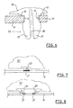
- the figures 3 to 6 show a detail of a shield 10, which on a To arrange printed circuit board 11 of the electronic module within the housing 1 is.
- the circuit board 11 has a recess 12 which for receiving a latching lug 13 of the shielding part 10 is formed.
- These Latch 13 is part of the shield 10 and can with this means a punching process are produced from a sheet metal part.
- the dimensions the locking lug 13 are initially chosen so that the locking lug 13 through the Recess 12 can be performed in the circuit board 11. However, that is Length of the locking lug 13 is greater than the thickness of the circuit board 11, so that the Latch 13 on the circuit board 11 protrudes.
- a punched arcuate projection 14 is present at the locking lug 13 at the locking lug 13 .
- This projection 14 is at the onset of the locking lug 13 in the recess 12th briefly pressed back, but jumps after the full onset of Latch 13 in the recess 12 back to its original position ( Figure 3, left representation), so that thereby the shielding member 10 on the circuit board 11 is set. It can not be easily removed now be, then it requires such a force that the resilient projection 14 is pushed back so far that the locking lug 13 from the recess 12 can be pulled out.
- the shielding part 10 has a Paragraph 15, which ensures that the shielding member 10 with his the PCB 11 facing lower circumferential edge is not completely on the Printed circuit board 11 rests, but a distance is given.
- This paragraph is 15 arranged according to Figure 3 right and left of the locking lug 13, but can also at any other locations on the lower edge of the shield 10 is present be.
- FIG. 4 shows a similar embodiment to FIG. 3, but here is one punched tab-shaped projection 16 present, which also at Inserting the locking lug 13 recedes into the recess 12 and after the full insertion jumps back, so that thereby the locking lug 13th is fixed to the circuit board 11. Also, the tab-shaped projection 16 can be produced easily and inexpensively by means of a stamping process.
- Figure 5 also shows a detent 13 which in the recess 12 of the circuit board 11 is used, however, the locking lug 13 here at least one point-shaped projection 17 (in particular two projections), through Compressive deformation can be produced and are arranged on the detent 13, that they after complete insertion of the locking lug 13 in the recess 12 at the lower edge of the circuit board 11 come to rest, so as well as the projections 14 and 16, the shielding member 10 on the circuit board 11 safely establish.
- the locking lug 13 here at least one point-shaped projection 17 (in particular two projections), through Compressive deformation can be produced and are arranged on the detent 13, that they after complete insertion of the locking lug 13 in the recess 12 at the lower edge of the circuit board 11 come to rest, so as well as the projections 14 and 16, the shielding member 10 on the circuit board 11 safely establish.
- the locking lug 13 is resilient.
- the locking lug 13 at least one slot 18, whereby two Form tabs 19 which have a greater longitudinal extent than the longitudinal extent the recess 12.
- the longitudinal extent of the two Tabs 19 and the width of the slot 18 is selected so that when inserting the Latch 13 in the recess 12, the two tabs 12 compressed and thus the locking lug 13 can be guided through the recess 12.
- the two tabs 19 spread apart again, while advantageously not assuming their original position, but stay under tension.
- the shielding 10 is under set a certain bias on the circuit board 11.
- the tabs 19 are in their upper region bevels, with which they at the lower edge of the circuit board 11 in the region of the recess 12th come to the plant.
- the tabs 19 are made oblique to a certain To ensure guidance during insertion.
- paragraphs 15 are shown in FIGS. 3 to 5, they can be seen in FIG be present in this form, but also elsewhere on the shielding be present or omitted altogether.
- Figures 7 and 8 show embodiments for the shielding part 10 with a contact surface on the circuit board 11 is electrically contacted.
- the shield member 10 at least one pressure tab 20, the for example, again punched out of the shielding and shaped.
- the punched and preformed pressure plate 20 is to some extent over the lower edge of the shielding member 10, so that it with a Contact surface 21 of the circuit board 11 comes under pretension to the plant and an electrical connection between the shielding part 10 and the contact surface 21 (ground connection) produces.
- Figure 6 shows a single pressure tab 20, the slightly angled at its end.
- FIG. 8 shows two opposite ones Pressure tabs 20, each with a contact surface 21 on the circuit board 11th are contacted.
- the presence of more than one pressure tab 20 has the Advantage that the contact safety is increased, in the event that a pressure flap 20 does not sufficiently contact the contact surface 21 or e.g. on reason Damage is deformed and thus no contact is given.
- FIGS. 9 and 10 show that the shielding part 10 serves as a shielding cage is trained.
- This shielding cage is on the circuit board in the above described manner and thus surrounds the electronic module, i. the electronic components, which are arranged on the circuit board, in order Shielding.
- This shielding cage is thus effectively prevented that on the one hand emitted by the electronic module interfering radiation, On the other hand, but also effectively prevents interference from outside, e.g. from other electronic modules, in that with the shielding cage shielded electronic module can radiate.
- each have a shielding cage or between which a shielding plate is arranged. Since to ensure the shield, the shielding on must have a certain electrical potential (in particular mass), According to the invention, the two alternatives for mounting and simultaneous electrical contacting proposed solutions realized. With view on FIGS. 9 and 10 can therefore have such a shielding part 10 with the corresponding ones trained locking lugs 13 easy and fast on the circuit board 11 (not here shown) mounted and dismounted. The electrical contact of the Shielding part 10 then takes place via the pressure tabs 20, which with contact surfaces 21 on the circuit board 11 correspond and / or on the spring plate 6, which on the shielding part 10 or on the inside of the housing.
- the shielding member 10 is electrically contacted with the housing 1. This contacting takes place in a particularly advantageous manner when the electronic Module is inserted with the shielding part 10 in the housing 1 or the electronic module is already mounted on a base plate of the housing 1 and then the housing 1 is mounted for closing.
- the inventive means for electrical contact between the Shielding part 10 and the housing 1 have the advantage in all variants that simple and inexpensive, especially in a stamping process or a Punching bending process, can be produced and at the same time disassembly exist remains, without it to a costly disassembly or destruction of the involved parts comes.
Landscapes
- Engineering & Computer Science (AREA)
- Microelectronics & Electronic Packaging (AREA)
- Shielding Devices Or Components To Electric Or Magnetic Fields (AREA)
- Control Of Motors That Do Not Use Commutators (AREA)
- Casings For Electric Apparatus (AREA)
Abstract
Description
- Figur 1:
- ein Gehäuse eines elektronischen Gerätes mit einem Federblech,
- Figur 2:
- Detailansichten des Federbleches,
- Figuren 3 bis 6:
- verschiedene Ausgestaltungen einer Rastanase,
- Figuren 7 und 8:
- Ausgestaltungen von Drucklaschen an dem Abschirmteil,
- Figuren 9 u. 10:
- Ansicht und Detailansicht eines als Abschirmkäfig ausgebildeten Abschirmteiles.
- 1.
- Gehäuse
- 2.
- Seitenteile
- 3.
- Öffnungen
- 4.
- Gewindebohrung
- 5.
- Gehäusedeckel
- 6.
- Federblech
- 7.
- Stift
- 8.
- Lasche
- 9.
- abgerundeter Endbereich
- 10.
- Abschirmteil
- 11.
- Leiterplatte
- 12.
- Ausnehmnung
- 13.
- Rastnase
- 14.
- ausgestanzter bogenförmiger Vorsprung
- 15.
- Absatz
- 16.
- ausgestanzter laschenförmiger Vorsprung
- 17.
- punktförmiger Vorsprung
- 18.
- Schlitz
- 19.
- Lasche
- 20.
- Drucklasche
- 21.
- Kontaktfläche
Claims (10)
- Elektronisches hochfrequenztechnisches Gerät mit einem Gehäuse (1) aus einem elektrisch leitfähigen Material, wobei in dem Gehäuse (1) zumindest ein elektronisches Modul sowie ein zugeordnetes Abschirmteil (10) angeordnet ist, dadurch gekennzeichnet, dass Mittel vorgesehen sind, die zwischen dem Gehäuse (1) und dem zumindest einen Abschirmteil (10) angeordnet sind und eine elektrische Kontaktierung zwischen dem Gehäuse (1) und dem zumindest einen Abschirmteil (10) herstellen.
- Gerät nach Anspruch 1, dadurch gekennzeichnet, dass die Mittel als ein Federblech (6) ausgebildet sind.
- Gerät nach Anspruch 2, dadurch gekennzeichnet, dass das Federblech (6) zumindest eine abstehende Lasche (8), insbesondere mehrere Laschen (8), aufweist.
- Gerät nach Anspruch 3, dadurch gekennzeichnet, dass die zumindest eine Lasche (8) einen abgerundeten Endbereich (9) aufweist.
- Gerät nach einem der vorhergehenden Ansprüche, dadurch gekennzeichnet, dass die Mittel, insbesondere das Federblech (6), lösbar oder unlösbar an dem Gehäuse (1) oder an dem Abschirmteil (10) befestigt sind.
- Elektronisches hochfrequenztechnisches Gerät mit einem Gehäuse (1) aus einem elektrisch leitfähigen Material, wobei in dem Gehäuse (1) zumindest ein elektronisches Modul sowie ein zugeordnetes Abschirmteil (10) angeordnet ist, dadurch gekennzeichnet, dass das Abschirmteil (10) Mittel zur lösbaren Befestigung an einer in dem Gehäuse (1) angeordneten Leiterplatte (11) aufweist.
- Gerät nach Anspruch 1, dadurch gekennzeichnet, dass die Mittel als eine Rastnase (13) ausgebildet sind.
- Gerät nach Anspruch 7, dadurch gekennzeichnet, dass die Rastnase (13) einen bogenförmigen, laschenförmigen oder punktförmigen Vorsprung (14, 15, 17) aufweist.
- Gerät nach Anspruch 7, dadurch gekennzeichnet, dass die Rastnase (13) federnd ausgebildet ist.
- Gerät nach einem der vorhergehenden Ansprüche, dadurch gekennzeichnet, dass das Abschirmteil (10) als Aschirmblech oder Abschirmkäfig ausgebildet ist.
Priority Applications (1)
| Application Number | Priority Date | Filing Date | Title |
|---|---|---|---|
| EP05013745A EP1603381B1 (de) | 2004-03-12 | 2005-03-05 | Federblech in einem Gehäuse als Abschirmung für ein elektronisches hochfrequenztechnisches Gerät |
Applications Claiming Priority (4)
| Application Number | Priority Date | Filing Date | Title |
|---|---|---|---|
| 1993-11-19 | |||
| DE102004012565 | 2004-03-12 | ||
| DE102004012565 | 2004-03-12 | ||
| DE200510010271 DE102005010271A1 (de) | 2004-03-12 | 2005-03-03 | Federblech in einem Gehäuse als Abschirmung für ein elektronisches hochfrequenztechnisches Gerät |
Related Child Applications (2)
| Application Number | Title | Priority Date | Filing Date |
|---|---|---|---|
| EP05013745A Division EP1603381B1 (de) | 2004-03-12 | 2005-03-05 | Federblech in einem Gehäuse als Abschirmung für ein elektronisches hochfrequenztechnisches Gerät |
| EP05013745.4 Division-Into | 2005-06-25 |
Publications (2)
| Publication Number | Publication Date |
|---|---|
| EP1575347A1 true EP1575347A1 (de) | 2005-09-14 |
| EP1575347B1 EP1575347B1 (de) | 2008-04-23 |
Family
ID=35079306
Family Applications (1)
| Application Number | Title | Priority Date | Filing Date |
|---|---|---|---|
| EP05004888A Expired - Lifetime EP1575347B1 (de) | 2004-03-12 | 2005-03-05 | Federblech in einem Gehäuse als Abschirmung für ein elektronisches hochfrequenztechnisches Gerät |
Country Status (3)
| Country | Link |
|---|---|
| EP (1) | EP1575347B1 (de) |
| AT (1) | ATE393566T1 (de) |
| DE (1) | DE502005003798D1 (de) |
Cited By (1)
| Publication number | Priority date | Publication date | Assignee | Title |
|---|---|---|---|---|
| DE102005046053B4 (de) | 2005-09-27 | 2021-11-18 | Robert Bosch Gmbh | Elektrische Vorrichtung mit einer Leiterplatte und einem Bauteil |
Citations (6)
| Publication number | Priority date | Publication date | Assignee | Title |
|---|---|---|---|---|
| DE3529105A1 (de) * | 1985-08-14 | 1987-02-19 | Philips Patentverwaltung | Geraeteeinsatz der nachrichtentechnik |
| EP0563673A1 (de) * | 1992-03-31 | 1993-10-06 | Siemens Aktiengesellschaft | Federblech zum grossflächigen Kontaktieren zweier Gehäuseteile |
| EP0696161A1 (de) * | 1994-08-01 | 1996-02-07 | Siemens Aktiengesellschaft | Anordnung zum Kontaktieren von Gehäuseteilen eines elektrischen Gerätes |
| EP0762822A1 (de) * | 1995-08-24 | 1997-03-12 | Siemens Nixdorf Informationssysteme AG | Vorrichtung zur Masseverbindung einer Flachbaugruppe |
| US6053771A (en) * | 1997-08-20 | 2000-04-25 | Dell Usa L.P. | Electromagnetic shield connector |
| EP1381264A1 (de) * | 2001-03-29 | 2004-01-14 | Sanyo Electric Co., Ltd. | Abschirmhülle |
-
2005
- 2005-03-05 AT AT05004888T patent/ATE393566T1/de not_active IP Right Cessation
- 2005-03-05 EP EP05004888A patent/EP1575347B1/de not_active Expired - Lifetime
- 2005-03-05 DE DE502005003798T patent/DE502005003798D1/de not_active Expired - Lifetime
Patent Citations (6)
| Publication number | Priority date | Publication date | Assignee | Title |
|---|---|---|---|---|
| DE3529105A1 (de) * | 1985-08-14 | 1987-02-19 | Philips Patentverwaltung | Geraeteeinsatz der nachrichtentechnik |
| EP0563673A1 (de) * | 1992-03-31 | 1993-10-06 | Siemens Aktiengesellschaft | Federblech zum grossflächigen Kontaktieren zweier Gehäuseteile |
| EP0696161A1 (de) * | 1994-08-01 | 1996-02-07 | Siemens Aktiengesellschaft | Anordnung zum Kontaktieren von Gehäuseteilen eines elektrischen Gerätes |
| EP0762822A1 (de) * | 1995-08-24 | 1997-03-12 | Siemens Nixdorf Informationssysteme AG | Vorrichtung zur Masseverbindung einer Flachbaugruppe |
| US6053771A (en) * | 1997-08-20 | 2000-04-25 | Dell Usa L.P. | Electromagnetic shield connector |
| EP1381264A1 (de) * | 2001-03-29 | 2004-01-14 | Sanyo Electric Co., Ltd. | Abschirmhülle |
Cited By (1)
| Publication number | Priority date | Publication date | Assignee | Title |
|---|---|---|---|---|
| DE102005046053B4 (de) | 2005-09-27 | 2021-11-18 | Robert Bosch Gmbh | Elektrische Vorrichtung mit einer Leiterplatte und einem Bauteil |
Also Published As
| Publication number | Publication date |
|---|---|
| DE502005003798D1 (de) | 2008-06-05 |
| ATE393566T1 (de) | 2008-05-15 |
| EP1575347B1 (de) | 2008-04-23 |
Similar Documents
| Publication | Publication Date | Title |
|---|---|---|
| DE69120688T2 (de) | Mehrpoliger abgeschirmter verbinder mit gemeinsamer erdung | |
| DE69411218T2 (de) | Halter für abgeschirmte Speicherkarte | |
| EP0965078B1 (de) | Trägeranordnung für elektronische baugruppen | |
| DE10006530A1 (de) | Antennenfeder | |
| DE10223170A1 (de) | EMV-Abschirmung für elektronische Bauelemente und EMV-Gehäuse | |
| DE102016122084A1 (de) | Elektronische Schaltungseinheit | |
| DE102015222874B4 (de) | System aus Gehäuse und Leiterplatte zum mechanischen Fixieren des Gehäuses | |
| WO1996031104A1 (de) | Steuergerät für ein kraftfahrzeug | |
| DE3627372A1 (de) | Kuehlkoerper fuer elektronische bauelemente | |
| WO2022053379A1 (de) | Gehäuse für eine auf einer leiterplatte angeordneten elektronische schaltung | |
| DE20112595U1 (de) | Gehäuse zur Aufnahme einer Leiterplatte mit elektronischen Bauteilen | |
| DE102016118630B3 (de) | Computersystem | |
| EP1705976B1 (de) | Messgerätmodul | |
| WO2007121834A1 (de) | Befestigungssystem, insbesondere für lampen | |
| DE102012005812A1 (de) | Elektrischer Verbinder mit integriertem Impedanzangleichelement | |
| EP1603381B1 (de) | Federblech in einem Gehäuse als Abschirmung für ein elektronisches hochfrequenztechnisches Gerät | |
| EP1575347A1 (de) | Federblech in einem Gehäuse als Abschirmung für ein elektronisches hochfrequenztechnisches Gerät | |
| DE102005010271A1 (de) | Federblech in einem Gehäuse als Abschirmung für ein elektronisches hochfrequenztechnisches Gerät | |
| DE102005033664A1 (de) | Federblech in einem Gehäuse als Abschirmung für ein elektronisches hochfrequenztechnisches Gerät | |
| DE102004013969A1 (de) | Optischer Verbinder | |
| EP1467608B1 (de) | Abschirmung für ein Hochfrquenzgerät, insbesondere einen TV-Tuner eines Fahrzeuges | |
| EP3652609B1 (de) | Computersystem, haltevorrichtung und montageverfahren für eine zusatzplatine in einem computersystem | |
| DE112018007953T5 (de) | Elektrisches Kontaktsystem und elektrische Vorrichtung mit einem elektrischen Kontaktsystem | |
| DE29721480U1 (de) | Gehäuse für ein elektronisches Gerät | |
| DE10008282B4 (de) | EMV-Kontaktierung |
Legal Events
| Date | Code | Title | Description |
|---|---|---|---|
| PUAI | Public reference made under article 153(3) epc to a published international application that has entered the european phase |
Free format text: ORIGINAL CODE: 0009012 |
|
| AK | Designated contracting states |
Kind code of ref document: A1 Designated state(s): AT BE BG CH CY CZ DE DK EE ES FI FR GB GR HU IE IS IT LI LT LU MC NL PL PT RO SE SI SK TR |
|
| AX | Request for extension of the european patent |
Extension state: AL BA HR LV MK YU |
|
| AKX | Designation fees paid | ||
| 17P | Request for examination filed |
Effective date: 20060509 |
|
| RBV | Designated contracting states (corrected) |
Designated state(s): AT BE BG CH CY CZ DE DK EE ES FI FR GB GR HU IE IS IT LI LT LU MC NL PL PT RO SE SI SK TR |
|
| 17Q | First examination report despatched |
Effective date: 20060626 |
|
| 17Q | First examination report despatched |
Effective date: 20060626 |
|
| GRAP | Despatch of communication of intention to grant a patent |
Free format text: ORIGINAL CODE: EPIDOSNIGR1 |
|
| GRAS | Grant fee paid |
Free format text: ORIGINAL CODE: EPIDOSNIGR3 |
|
| GRAA | (expected) grant |
Free format text: ORIGINAL CODE: 0009210 |
|
| AK | Designated contracting states |
Kind code of ref document: B1 Designated state(s): AT BE BG CH CY CZ DE DK EE ES FI FR GB GR HU IE IS IT LI LT LU MC NL PL PT RO SE SI SK TR |
|
| REG | Reference to a national code |
Ref country code: GB Ref legal event code: FG4D Free format text: NOT ENGLISH |
|
| REG | Reference to a national code |
Ref country code: CH Ref legal event code: EP |
|
| REF | Corresponds to: |
Ref document number: 502005003798 Country of ref document: DE Date of ref document: 20080605 Kind code of ref document: P |
|
| REG | Reference to a national code |
Ref country code: IE Ref legal event code: FG4D Free format text: LANGUAGE OF EP DOCUMENT: GERMAN |
|
| PG25 | Lapsed in a contracting state [announced via postgrant information from national office to epo] |
Ref country code: SI Free format text: LAPSE BECAUSE OF FAILURE TO SUBMIT A TRANSLATION OF THE DESCRIPTION OR TO PAY THE FEE WITHIN THE PRESCRIBED TIME-LIMIT Effective date: 20080423 |
|
| NLV1 | Nl: lapsed or annulled due to failure to fulfill the requirements of art. 29p and 29m of the patents act | ||
| ET | Fr: translation filed | ||
| PG25 | Lapsed in a contracting state [announced via postgrant information from national office to epo] |
Ref country code: NL Free format text: LAPSE BECAUSE OF FAILURE TO SUBMIT A TRANSLATION OF THE DESCRIPTION OR TO PAY THE FEE WITHIN THE PRESCRIBED TIME-LIMIT Effective date: 20080423 Ref country code: PT Free format text: LAPSE BECAUSE OF FAILURE TO SUBMIT A TRANSLATION OF THE DESCRIPTION OR TO PAY THE FEE WITHIN THE PRESCRIBED TIME-LIMIT Effective date: 20080923 Ref country code: ES Free format text: LAPSE BECAUSE OF FAILURE TO SUBMIT A TRANSLATION OF THE DESCRIPTION OR TO PAY THE FEE WITHIN THE PRESCRIBED TIME-LIMIT Effective date: 20080803 Ref country code: FI Free format text: LAPSE BECAUSE OF FAILURE TO SUBMIT A TRANSLATION OF THE DESCRIPTION OR TO PAY THE FEE WITHIN THE PRESCRIBED TIME-LIMIT Effective date: 20080423 Ref country code: BG Free format text: LAPSE BECAUSE OF FAILURE TO SUBMIT A TRANSLATION OF THE DESCRIPTION OR TO PAY THE FEE WITHIN THE PRESCRIBED TIME-LIMIT Effective date: 20080723 |
|
| PG25 | Lapsed in a contracting state [announced via postgrant information from national office to epo] |
Ref country code: PL Free format text: LAPSE BECAUSE OF FAILURE TO SUBMIT A TRANSLATION OF THE DESCRIPTION OR TO PAY THE FEE WITHIN THE PRESCRIBED TIME-LIMIT Effective date: 20080423 |
|
| REG | Reference to a national code |
Ref country code: IE Ref legal event code: FD4D |
|
| PG25 | Lapsed in a contracting state [announced via postgrant information from national office to epo] |
Ref country code: IS Free format text: LAPSE BECAUSE OF FAILURE TO SUBMIT A TRANSLATION OF THE DESCRIPTION OR TO PAY THE FEE WITHIN THE PRESCRIBED TIME-LIMIT Effective date: 20080823 |
|
| PG25 | Lapsed in a contracting state [announced via postgrant information from national office to epo] |
Ref country code: LT Free format text: LAPSE BECAUSE OF FAILURE TO SUBMIT A TRANSLATION OF THE DESCRIPTION OR TO PAY THE FEE WITHIN THE PRESCRIBED TIME-LIMIT Effective date: 20080423 Ref country code: IE Free format text: LAPSE BECAUSE OF FAILURE TO SUBMIT A TRANSLATION OF THE DESCRIPTION OR TO PAY THE FEE WITHIN THE PRESCRIBED TIME-LIMIT Effective date: 20080423 Ref country code: DK Free format text: LAPSE BECAUSE OF FAILURE TO SUBMIT A TRANSLATION OF THE DESCRIPTION OR TO PAY THE FEE WITHIN THE PRESCRIBED TIME-LIMIT Effective date: 20080423 Ref country code: CZ Free format text: LAPSE BECAUSE OF FAILURE TO SUBMIT A TRANSLATION OF THE DESCRIPTION OR TO PAY THE FEE WITHIN THE PRESCRIBED TIME-LIMIT Effective date: 20080423 Ref country code: SE Free format text: LAPSE BECAUSE OF FAILURE TO SUBMIT A TRANSLATION OF THE DESCRIPTION OR TO PAY THE FEE WITHIN THE PRESCRIBED TIME-LIMIT Effective date: 20080723 |
|
| PG25 | Lapsed in a contracting state [announced via postgrant information from national office to epo] |
Ref country code: SK Free format text: LAPSE BECAUSE OF FAILURE TO SUBMIT A TRANSLATION OF THE DESCRIPTION OR TO PAY THE FEE WITHIN THE PRESCRIBED TIME-LIMIT Effective date: 20080423 Ref country code: RO Free format text: LAPSE BECAUSE OF FAILURE TO SUBMIT A TRANSLATION OF THE DESCRIPTION OR TO PAY THE FEE WITHIN THE PRESCRIBED TIME-LIMIT Effective date: 20080423 |
|
| PLBE | No opposition filed within time limit |
Free format text: ORIGINAL CODE: 0009261 |
|
| STAA | Information on the status of an ep patent application or granted ep patent |
Free format text: STATUS: NO OPPOSITION FILED WITHIN TIME LIMIT |
|
| 26N | No opposition filed |
Effective date: 20090126 |
|
| PG25 | Lapsed in a contracting state [announced via postgrant information from national office to epo] |
Ref country code: EE Free format text: LAPSE BECAUSE OF FAILURE TO SUBMIT A TRANSLATION OF THE DESCRIPTION OR TO PAY THE FEE WITHIN THE PRESCRIBED TIME-LIMIT Effective date: 20080423 |
|
| PG25 | Lapsed in a contracting state [announced via postgrant information from national office to epo] |
Ref country code: IT Free format text: LAPSE BECAUSE OF FAILURE TO SUBMIT A TRANSLATION OF THE DESCRIPTION OR TO PAY THE FEE WITHIN THE PRESCRIBED TIME-LIMIT Effective date: 20080423 |
|
| BERE | Be: lapsed |
Owner name: HIRSCHMANN ELECTRONICS G.M.B.H. Effective date: 20090331 |
|
| PG25 | Lapsed in a contracting state [announced via postgrant information from national office to epo] |
Ref country code: MC Free format text: LAPSE BECAUSE OF NON-PAYMENT OF DUE FEES Effective date: 20090331 |
|
| REG | Reference to a national code |
Ref country code: CH Ref legal event code: PL |
|
| PG25 | Lapsed in a contracting state [announced via postgrant information from national office to epo] |
Ref country code: CH Free format text: LAPSE BECAUSE OF NON-PAYMENT OF DUE FEES Effective date: 20090331 Ref country code: LI Free format text: LAPSE BECAUSE OF NON-PAYMENT OF DUE FEES Effective date: 20090331 |
|
| PG25 | Lapsed in a contracting state [announced via postgrant information from national office to epo] |
Ref country code: BE Free format text: LAPSE BECAUSE OF NON-PAYMENT OF DUE FEES Effective date: 20090331 |
|
| PG25 | Lapsed in a contracting state [announced via postgrant information from national office to epo] |
Ref country code: AT Free format text: LAPSE BECAUSE OF NON-PAYMENT OF DUE FEES Effective date: 20090305 |
|
| PG25 | Lapsed in a contracting state [announced via postgrant information from national office to epo] |
Ref country code: GR Free format text: LAPSE BECAUSE OF FAILURE TO SUBMIT A TRANSLATION OF THE DESCRIPTION OR TO PAY THE FEE WITHIN THE PRESCRIBED TIME-LIMIT Effective date: 20080724 |
|
| PG25 | Lapsed in a contracting state [announced via postgrant information from national office to epo] |
Ref country code: LU Free format text: LAPSE BECAUSE OF NON-PAYMENT OF DUE FEES Effective date: 20090305 |
|
| PG25 | Lapsed in a contracting state [announced via postgrant information from national office to epo] |
Ref country code: HU Free format text: LAPSE BECAUSE OF FAILURE TO SUBMIT A TRANSLATION OF THE DESCRIPTION OR TO PAY THE FEE WITHIN THE PRESCRIBED TIME-LIMIT Effective date: 20081024 |
|
| PG25 | Lapsed in a contracting state [announced via postgrant information from national office to epo] |
Ref country code: TR Free format text: LAPSE BECAUSE OF FAILURE TO SUBMIT A TRANSLATION OF THE DESCRIPTION OR TO PAY THE FEE WITHIN THE PRESCRIBED TIME-LIMIT Effective date: 20080423 |
|
| PG25 | Lapsed in a contracting state [announced via postgrant information from national office to epo] |
Ref country code: CY Free format text: LAPSE BECAUSE OF FAILURE TO SUBMIT A TRANSLATION OF THE DESCRIPTION OR TO PAY THE FEE WITHIN THE PRESCRIBED TIME-LIMIT Effective date: 20080423 |
|
| REG | Reference to a national code |
Ref country code: DE Ref legal event code: R081 Ref document number: 502005003798 Country of ref document: DE Owner name: HIRSCHMANN CAR COMMUNICATION GMBH, DE Free format text: FORMER OWNER: HIRSCHMANN ELECTRONICS GMBH, 72654 NECKARTENZLINGEN, DE Effective date: 20120531 Ref country code: DE Ref legal event code: R082 Ref document number: 502005003798 Country of ref document: DE Representative=s name: THUL PATENTANWALTSGESELLSCHAFT MBH, DE Effective date: 20120531 |
|
| REG | Reference to a national code |
Ref country code: FR Ref legal event code: TP Owner name: HIRSCHMANN CAR COMMUNICATION GMBH, DE Effective date: 20120802 |
|
| REG | Reference to a national code |
Ref country code: GB Ref legal event code: 732E Free format text: REGISTERED BETWEEN 20120809 AND 20120815 |
|
| REG | Reference to a national code |
Ref country code: FR Ref legal event code: PLFP Year of fee payment: 12 |
|
| REG | Reference to a national code |
Ref country code: FR Ref legal event code: PLFP Year of fee payment: 13 |
|
| REG | Reference to a national code |
Ref country code: FR Ref legal event code: PLFP Year of fee payment: 14 |
|
| REG | Reference to a national code |
Ref country code: DE Ref legal event code: R082 Ref document number: 502005003798 Country of ref document: DE Representative=s name: WILHELM & BECK, DE |
|
| PGFP | Annual fee paid to national office [announced via postgrant information from national office to epo] |
Ref country code: FR Payment date: 20230110 Year of fee payment: 19 |
|
| PGFP | Annual fee paid to national office [announced via postgrant information from national office to epo] |
Ref country code: GB Payment date: 20230112 Year of fee payment: 19 Ref country code: DE Payment date: 20230110 Year of fee payment: 19 |
|
| REG | Reference to a national code |
Ref country code: DE Ref legal event code: R119 Ref document number: 502005003798 Country of ref document: DE |
|
| GBPC | Gb: european patent ceased through non-payment of renewal fee |
Effective date: 20240305 |
|
| PG25 | Lapsed in a contracting state [announced via postgrant information from national office to epo] |
Ref country code: DE Free format text: LAPSE BECAUSE OF NON-PAYMENT OF DUE FEES Effective date: 20241001 |
|
| PG25 | Lapsed in a contracting state [announced via postgrant information from national office to epo] |
Ref country code: GB Free format text: LAPSE BECAUSE OF NON-PAYMENT OF DUE FEES Effective date: 20240305 |
|
| PG25 | Lapsed in a contracting state [announced via postgrant information from national office to epo] |
Ref country code: FR Free format text: LAPSE BECAUSE OF NON-PAYMENT OF DUE FEES Effective date: 20240331 |
|
| PG25 | Lapsed in a contracting state [announced via postgrant information from national office to epo] |
Ref country code: GB Free format text: LAPSE BECAUSE OF NON-PAYMENT OF DUE FEES Effective date: 20240305 Ref country code: FR Free format text: LAPSE BECAUSE OF NON-PAYMENT OF DUE FEES Effective date: 20240331 Ref country code: DE Free format text: LAPSE BECAUSE OF NON-PAYMENT OF DUE FEES Effective date: 20241001 |