EP1575304B1 - Farbabbildungselement, farbfiltergruppe und farbabbildungseinrichtung - Google Patents
Farbabbildungselement, farbfiltergruppe und farbabbildungseinrichtung Download PDFInfo
- Publication number
- EP1575304B1 EP1575304B1 EP03778803A EP03778803A EP1575304B1 EP 1575304 B1 EP1575304 B1 EP 1575304B1 EP 03778803 A EP03778803 A EP 03778803A EP 03778803 A EP03778803 A EP 03778803A EP 1575304 B1 EP1575304 B1 EP 1575304B1
- Authority
- EP
- European Patent Office
- Prior art keywords
- pixel
- color
- light
- sensitivity
- range
- Prior art date
- Legal status (The legal status is an assumption and is not a legal conclusion. Google has not performed a legal analysis and makes no representation as to the accuracy of the status listed.)
- Expired - Lifetime
Links
Images

Classifications
-
- H—ELECTRICITY
- H04—ELECTRIC COMMUNICATION TECHNIQUE
- H04N—PICTORIAL COMMUNICATION, e.g. TELEVISION
- H04N23/00—Cameras or camera modules comprising electronic image sensors; Control thereof
- H04N23/10—Cameras or camera modules comprising electronic image sensors; Control thereof for generating image signals from different wavelengths
-
- H—ELECTRICITY
- H04—ELECTRIC COMMUNICATION TECHNIQUE
- H04N—PICTORIAL COMMUNICATION, e.g. TELEVISION
- H04N25/00—Circuitry of solid-state image sensors [SSIS]; Control thereof
- H04N25/10—Circuitry of solid-state image sensors [SSIS]; Control thereof for transforming different wavelengths into image signals
- H04N25/11—Arrangement of colour filter arrays [CFA]; Filter mosaics
- H04N25/13—Arrangement of colour filter arrays [CFA]; Filter mosaics characterised by the spectral characteristics of the filter elements
- H04N25/135—Arrangement of colour filter arrays [CFA]; Filter mosaics characterised by the spectral characteristics of the filter elements based on four or more different wavelength filter elements
-
- H—ELECTRICITY
- H04—ELECTRIC COMMUNICATION TECHNIQUE
- H04N—PICTORIAL COMMUNICATION, e.g. TELEVISION
- H04N2209/00—Details of colour television systems
- H04N2209/04—Picture signal generators
- H04N2209/041—Picture signal generators using solid-state devices
- H04N2209/042—Picture signal generators using solid-state devices having a single pick-up sensor
- H04N2209/045—Picture signal generators using solid-state devices having a single pick-up sensor using mosaic colour filter
-
- H—ELECTRICITY
- H10—SEMICONDUCTOR DEVICES; ELECTRIC SOLID-STATE DEVICES NOT OTHERWISE PROVIDED FOR
- H10F—INORGANIC SEMICONDUCTOR DEVICES SENSITIVE TO INFRARED RADIATION, LIGHT, ELECTROMAGNETIC RADIATION OF SHORTER WAVELENGTH OR CORPUSCULAR RADIATION
- H10F39/00—Integrated devices, or assemblies of multiple devices, comprising at least one element covered by group H10F30/00, e.g. radiation detectors comprising photodiode arrays
- H10F39/80—Constructional details of image sensors
- H10F39/805—Coatings
- H10F39/8053—Colour filters
Definitions
- the present invention relates to a color image sensor and a color filter array which are applied to a color imaging device such as an electronic camera and a video camera, and the color imaging device.
- a color image sensor has been conventionally applied to a color imaging device such as an electronic camera and a video camera.
- the color imaging device In general, it is preferable for the color imaging device to bring spectral sensitivity characteristics of its imaging optical system from a shooting lens to a color image sensor closer to spectral sensitivity characteristics of the eyes of a human being (or color matching functions which are publicly known) as much as possible.
- the color image sensor has a G pixel detecting green light, a B pixel detecting blue light, and an R pixel detecting red light, which are arranged in an array state.
- a Bayer matrix has the G pixels arranged in a checkered pattern and the B pixel and R pixel arranged alternately in gaps between the G pixels. That is, one unit (pixel block) is constituted of the four pixels made of the two G pixels, one B pixel, and one R pixel.
- the reason why the number of the G pixels is greater than the R pixel and B pixel is as follows.
- One of characteristics of the eyes of the human being is that the number of cells detecting green is greater than the number of cells detecting other colors. Accordingly, the eyes of the human being have wide detection luminance range of the green light. Accordingly, when a large quantity of the G pixels are provided in the image sensor, it is possible to extend the detection luminance range (what is called dynamic range) similarly to the eyes of the human being.
- color range to be discriminated by the three kinds of pixels which are the R pixel, G pixel, and B pixel
- the color range to be discriminated by the eyes of the human being is slightly narrower than the color range to be discriminated by the eyes of the human being, two different colors for the eyes of the human being are sometimes detected as the same color.
- a Y pixel detecting color between green and red (yellow) is added in addition to the R pixel, G pixel, and B pixel, to thereby enlarge detection color range.
- this problem is not caused when the color image sensor is changed to a multi-board type because the Y pixel can be added without reducing the number of the G pixels, but it is not so suitable for the electronic camera and video camera requiring downsizing, because an arrangement space is increased from the necessity for branching an optical path and arranging the image sensor for each branched path.
- JP-A-2001016598 and JP-A-3174890 disclose a color imaging device comprising second green color component G2 having a peak sensitivity near the peak of a minus sensitivity of the red of an ideal sensitivity.
- a color imaging device is defined in claim 1. It comprises a color image sensor in which pixel blocks are arranged in an array state, comprising a first pixel detecting red light, a second pixel detecting green light, a third pixel detecting blue light, and a fourth pixel detecting light having a wavelength between the green light and the blue light or between the green light and the red light, wherein sensitivity of the fourth pixel to the above-mentioned light is kept lower than sensitivity of the second pixel to the green light.
- the detection color range is enlarged. Further, when an output of the fourth pixel is referred to in addition to an output of the second pixel, it is possible to detect the high-level green light. Accordingly, the reduction of the detection luminance range can be suppressed while enlarging the detection color range.
- the sensitivity of the fourth pixel is kept to about half the sensitivity of the second pixel.
- a peak wavelength of a sensitivity characteristic of the first pixel is within the range from 590 nm to 640 nm
- a peak wavelength of a sensitivity characteristic of the second pixel is within the range from 520 nm to 570 nm
- a peak wavelength of a sensitivity characteristic of the third pixel is within the range from 430 nm to 480 nm
- a peak wavelength of a sensitivity characteristic of the fourth pixel is within the range from 490 nm to 530 nm or the range from 560 nm to 640 nm.
- a color filter array comprises filter blocks arranged in an array state, comprising a first filter unit limiting incident visible light to red light, a second filter unit limiting the incident visible light to green, a third filter unit limiting the incident visible light to blue light, and a fourth filter unit limiting the incident visible light to light having a wavelength between the green light and the blue light or between the green light and the red light, wherein transmittance of the fourth filter unit to the above-mentioned light is kept lower than transmittance of the second filter unit to the green light.
- the detection color range of the color mage sensor is enlarged. Further, when an output of the pixel opposing the fourth filter unit is referred to in addition to an output of the pixel opposing the second filter unit of the color image sensor, it is possible to detect the high-level green light. Accordingly, when this color filter array is used, the color image sensor which can suppress the reduction of the detection luminance range while enlarging the detection color range is realized.
- the transmittance of the fourth filter unit is kept to about half the transmittance of the second filter unit.
- a peak wavelength of a transmittance characteristic of the first filter unit in a visible light region is within the range from 590 nm to 640 nm
- a peak wavelength of a transmittance characteristic of the second filter unit in the visible light region is within the range from 520 nm to 570 nm
- a peak wavelength of a transmittance characteristic of the third filter unit in the visible light region is within the range from 430 nm to 480 nm
- a peak wavelength of a transmittance characteristic of the fourth filter unit in the visible light region is within the range from 490 nm to 530 nm or the range from 560 nm to 640 nm.
- This embodiment relates to an electronic camera (corresponding to a color imaging device of the present invention) to which a color image sensor of the present invention or a color filter array of the present invention is applied.
- Fig. 1 is a view showing schematic structure of the electronic camera of this embodiment.
- the electronic camera is constituted of, for example, an electronic camera body 1 and a shooting lens 2.
- the electronic camera body 1 is provided with a color image sensor 11, an A/D converter 12, a white balance processing circuit 14, a color interpolation circuit 15, a color transformation circuit 16, a color transformation matrix decision circuit 13 (corresponding to a signal processing unit) and the like.
- a subject image by the shooting lens 2 is formed on the color image sensor 11.
- An output signal from the color image sensor 11 is inputted into the A/D converter 12 via a not-shown analog gain controller, and converted into a digital signal.
- the digital signal is subjected to white balance processing in the white balance processing circuit 14, color interpolation processing in the interpolation circuit 15, gray-scale transformation processing in the color transformation circuit 16, and then stored in a not-shown memory.
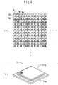
- Figs. 2 are views explaining the color image sensor 11 of this embodiment.
- Fig. 2(a) is a view explaining respective pixel blocks B and respective pixels P of the color image sensor 11
- Fig. 2(b) is a view showing a structural example of the color image sensor 11.
- the pixel blocks B are arranged in an array state on an imaging surface of the color image sensor 11.
- Each pixel block B has an R pixel Pr for detecting red light (corresponding to a first pixel), a G1 pixel Pg1 for detecting green light (corresponding to a second pixel), a B pixel Pb for detecting blue light (corresponding to a third pixel), and a G2 pixel Pg2 for detecting light having a wavelength between the green light and blue light (corresponding to a fourth pixel) which are arranged in a cross shape.
- the sensitivity of the G2 pixel Pg2 to the above-mentioned light is set lower than the sensitivity of the G1 pixel Pg1 to the green light.
- the G1 pixel Pg1 and the G2 pixel Pg2 are arranged to have the relation unadjacent to each other in each pixel block B (that is, upper right-lower left relation as shown in the drawing, or upper left-lower right relation).
- the electronic camera of this embodiment may treat an output of the G1 pixel Pg1 and an output of the G2 pixel Pg2 as the outputs of the pixels of different kinds or the outputs of the pixels of the same kind, and therefore it is preferable that the G1 pixel Pg1 and the G2 pixel Pg2 are arranged alternately and in a checkered pattern on the imaging surface.
- the color image sensor 1 like the above is constituted by, for example, preparing an image sensor 11a for capturing a visible light image (which is hereinafter a monochrome image sensor in which characteristics of respective pixels are equal to each other) and arranging a color filter array 11b on the incident side of the image sensor 11a.
- a visible light image which is hereinafter a monochrome image sensor in which characteristics of respective pixels are equal to each other
- the color filter array 11b has filter blocks arranged in an array state, and each of the filter blocks has an R filter unit for limiting the incident visible light to the red light, a G1 filter unit for limiting the incident visible light to green, a B filter unit for limiting the incident visible light to the blue light, and a G2 filter unit for limiting the incident visible light to the light having the wavelength between the green light and the blue light, being arranged.
- the transmittance of the G2 filter unit to the above-mentioned light is set lower than the transmittance of the G1 filter unit to the green light.
- the pixel of the image sensor 11b opposing the R filter unit can be used as the R pixel Pr for detecting the red light
- the pixel opposing the G1 filter unit can be used as the G1 pixel Pg1 for detecting the green light
- the pixel opposing the B filter unit can be used as the B pixel Pb for detecting the blue light
- the pixel opposing the G2 filter unit can be used as the G2 pixel Pg2 for detecting the light having the wavelength between the green light and the blue light.
- the G1 filter unit and the G2 filter unit are arranged to have the relation unadjacent to each other in each filter block (that is, upper right-lower left relation or upper left-lower right relation), in order to arrange the G1 pixel Pg1 and the G2 pixel Pg2 in the checkered pattern.
- Fig. 3 is a graph showing spectral sensitivity characteristics of the color image sensor 11 of this embodiment.
- the curve denoted by the symbol “R” corresponds to a sensitivity characteristic curve of the R pixel Pr
- the curve denoted by the symbol “G1” corresponds to a sensitivity characteristic curve of the G1 pixel Pg1
- the curve denoted by the symbol “B” corresponds to a sensitivity characteristic curve of the B pixel Pb
- the curve denoted by the symbol “G2” corresponds to a sensitivity characteristic curve of the G2 pixel Pg2.
- a peak wavelength of the sensitivity characteristic of the R pixel Pr for detecting the red light is within the range from 590 nm to 640 nm
- a peak wavelength of the sensitivity characteristic of the G1 pixel Pg1 for detecting the green light is within the range from 520 nm to 570 nm
- a peak wavelength of the sensitivity characteristic of the B pixel Pb for detecting the blue light is within the range from 430 nm to 480 nm.
- a peak wavelength of the sensitivity characteristic of the G2 pixel Pg2 for detecting the light between the blue light and the green light is within the range from 490 nm to 530 nm.
- the peak wavelength of the sensitivity characteristic of the R pixel Pr is 600 nm
- the peak wavelength of the sensitivity characteristic of the G1 pixel Pg1 is 540 nm
- the peak wavelength of the sensitivity characteristic of the B pixel Pb is 460 nm
- the peak wavelength of the sensitivity characteristic of the G2 pixel Pg2 is 500 nm.
- spectral transmittance characteristics of the color filter array 11b for adding such spectral sensitivity characteristics to the color image sensor 11 are as follows.
- a peak wavelength of the transmittance characteristic of the R filter unit of the color filter array 11b is within the range from 590 nm to 640 nm
- a peak wavelength of the sensitivity characteristic of the G1 filter unit is within the range from 520 nm to 570 nm
- a peak wavelength of the sensitivity characteristic of the B filter unit is within the range from 430 nm to 480 nm.
- a peak wavelength of the sensitivity characteristic of the G2 filter unit is within the range from 490 nm to 530 nm.
- the peak wavelength of the transmittance characteristic of the R filter unit is 600 nm
- the peak wavelength of the transmittance characteristic of the G 1 filter unit is 540 nm
- the peak wavelength of the transmittance characteristic of the B filter unit is 460 nm
- the peak wavelength of the transmittance characteristic of the G2 filter unit is 500 nm.
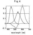
- Fig. 4 is a graph showing color matching functions (publicly known).
- the sensitivity characteristic of the R pixel, the sensitivity characteristic of the G1 pixel, and the sensitivity characteristic of the B pixel of this embodiment correspond to the color matching function r, the color matching function g and the color matching function b, respectively.
- the color matching function r has not only a positive peak, but also a negative peak.
- the sensitivity characteristic of the G2 pixel of this embodiment has its peak at the position corresponding to the negative peak of the color matching function r.
- color detection in color range which is almost the same as the color range shown by the color matching functions r, g and b (that is, the color range detectable by the eyes of a human being) is possible, based on the output value of the R pixel, the output value of the G1 pixel, the output value of the B pixel, and an opposite sign of the output value of the G2 pixel.
- the sensitivity of the G2 pixel is positively set lower than the sensitivity of the G1 pixel.
- the sensitivity of the G2 pixel is about half the sensitivity of the G1 pixel.
- a saturation level of the G2 pixel becomes higher than a saturation level of the G1 pixel (value showing the upper limit of detectable luminance), and is set approximately twice as high.
- the color interpolation circuit 15 shown in Fig. 1 performs color interpolation based on an output signal R of the R pixel Pr, an output signal G1 of the G1 pixel Pg1, an output signal B of the B pixel Pb, and an output signal G2 of the G2 pixel Pg2 (incidentally, these are the output signals after the A/D conversion and white balance processing), and generates signals (R, G1, G2 and B) showing respective color components of the light incident on each pixel (pixel signals).
- the G1 component, G2 component, and B component in the pixel signal of the R pixel in a pixel block B are respectively obtained based on the respective output signals of the G1 pixel, G2 pixel, and B pixel in the surrounding pixel block.
- the R component, G2 component, and B component in the pixel signal of the G1 pixel in a pixel block B are respectively obtained based on the respective output signals of the R pixel, G2 pixel, and B pixel in the surrounding pixel block.
- the R component, G1 component, and B component in the pixel signal of the G2 pixel in a pixel block B are respectively obtained based on the respective output signals of the R pixel, G1 pixel, and B pixel in the surrounding pixel block.
- the R component, G1 component, and G2 component in the pixel signal of the B pixel in a pixel block B are respectively obtained based on the respective output signals of the R pixel, G1 pixel, and G2 pixel in the surrounding pixel block.
- the color transformation circuit 16 subjects the pixel signals (R, G1, G2 and B) to the color transformation by multiplying these by a color transformation matrix M of 3 x 4, as shown in the expression (1), to generate color signals for display (R, G and B).
- R G B M R G ⁇ 1 G ⁇ 2 B
- the color transformation matrix M to be multiplied by the color transformation circuit 16 of this embodiment is any one of a matrix A, matrix B, and matrix C.
- the matrix A, matrix B or matrix C is set selectively by the color transformation matrix decision circuit 13.
- the color transformation matrix decision circuit 13 refers to the G1 component of the pixel signals (R, G1, G2 and B) and makes a selection based on the value of the G1 component. Further, as a result of the selection, the color transformation matrix decision circuit 13 performs white balance reprocessing if necessary (as will be described later in detail).
- the matrixes A, B and C are expressed by the expressions (2), (3) and (4), for example.
- A 0.60 0.66 - 1.25 0.31 0.23 1.15 - 0.87 0.04 0.02 0.14 - 0.65 1.01
- B 0.64 0.44 - 0.63 0.18 0.26 1.00 - 0.43 - 0.05 0.00 0.03 - 0.32 0.94
- C 0.67 0 0.23 0.06 0.28 0 0.85 - 0.14 0.02 0 - 0.09 0.88
- the matrix A or the matrix B reflects the respective components of the pixel signals (R, G1, G2 and B) in the color signals (R, G and B).
- the peaks of the sensitivity characteristic of the G 1 pixel and the sensitivity characteristic of the G2 pixel are close to each other. Therefore, the G1 component and G2 component show a subtle color difference precisely.
- the matrix A or matrix B reflects the subtle color difference of the pixel signals (R, G1, G2 and B) in the color signals (R, G and B) precisely.
- the matrix C regards the G2 component as the signal showing green, instead of the G1 component of the pixel signals (R, G1, G2 and B), and reflects the R component, G2 component, and B component in the color signals (R, G and B).
- the peaks of the sensitivity characteristic of the G1 pixel and the sensitivity characteristic of the G2 pixel are close to each other, and the saturation level of the G2 pixel is higher than the saturation level of the G 1 pixel (twice as high). Accordingly, the G2 component shows the luminance of the color close to the color shown by the G 1 component (green) precisely up to the level higher than the G 1 component.
- the matrix C reflects the high level luminance of the pixel signals (R, G1, G2 and B) in the color signals (R, G and B) precisely.
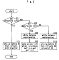
- Fig. 5 is a flowchart explaining the procedure of the processing by the color transformation matrix decision circuit 13.
- the color transformation matrix decision circuit 13 refers to the G1 component of the pixel signals (R, G1, G2 and B).
- the value of the G1 component does not exceed the saturation level (value corresponding to the saturation level of the output signal of the G1 pixel, which is 3500, for example) (YES in a step S11, or NO and YES in a step S12), it selects the matrix A or the matrix B which reflects the subtle color difference precisely (a step S21 or step S22), and when the value of the G1 component exceeds the saturation level (3500, for example) (NO in the step S11 and NO in the step S12), it selects the matrix C which reflects the high level luminance precisely (a step S23).
- the detection color range enlarges, and when the value of the G1 component of the pixel signals (R, G 1, G2 and B) exceeds the saturation level of the G1 pixel (NO in the step S11 and NO in the step S12), the high luminance can be detected precisely although the detection color range does not enlarge. Therefore, reduction of the detection luminance range can be suppressed while enlarging the detection color range.
- the absolute values of the coefficients in the second column (coefficients of G1) and the coefficients in the third column (coefficients of G2) of the matrix B are smaller than those of the matrix A as a whole (the matrix B has the smaller reflection amount of the G1 components and the smaller negative reflection amount of the G2 components than the matrix A).
- the matrix B performs the color transformation between the matrix A and the matrix C (the reflection amount of the G1 components is 0 and the reflection amount of the G2 components is large).
- the matrix A is selected (a step S21) when the value of the G1 component is lower than a threshold value (3000, for example) which is smaller than the saturation level (YES in the step S11), and the matrix B is selected (a step S22) when it is higher than the threshold value and lower than the saturation level (NO in the step S11 and YES in the step S11).
- the white balance gain to be multiplied by the respective signals by the white balance processing circuit 14 (refer to Fig. 1 ) is supposed to be an optimum value when using the matrix A.
- the white balance reprocessing is performed before the step S22 and the step S23 are performed (steps S32 and S33).
- the white balance gain to be multiplied in the white balance reprocessing in the step S32 is an optimum value when using the matrix B instead of the matrix A
- the white balance gain to be multiplied in the white balance reprocessing in the step S33 is an optimum value when using the matrix C instead of the matrix A.
- the sensitivity of the G2 pixel is "half" the sensitivity of the G1 pixel in the above-described embodiment
- processing attaching a higher value to "enlargement of the detection color range” than “suppressing the reduction of the detection luminance range” is possible when it is set to be slightly larger than the half
- processing attaching a higher value to "suppressing the reduction of the detection luminance range” than “enlargement of the detection color range” is possible when it is set to be slightly smaller than the half.
- the relation between the G2 sensitivity and the G1 sensitivity is decided by taking a balance between the two in consideration.
- the detection color of the G2 pixel is the color between blue and green in the above-described embodiment
- the same effects as those of the above-described embodiment can be obtained even when it is changed to color between green and red, as long as its sensitivity is set lower than the G1 pixel (preferably about a half).
- the contents of the color transformation matrixes are changed appropriately according to the sensitivity characteristic of the G2 pixel.
- the color image sensor in which the color filter array and the monochrome image sensor are combined is exemplified in the above-described embodiment, it is possible to use a color image sensor which does not use the color filter. Further, when a new color filter array is arranged on a conventional color image sensor (such as a color image sensor having a Bayer matrix and the like), it is also possible to add the spectral sensitivity characteristics similar to those of the color image sensor according to the above-described embodiment.
- a single board type color image sensor which can suppress the reduction of the detection luminance range while enlarging the detection color range is realized.
- the color filter array which can suppress the reduction of the detection luminance range while enlarging the detection color range is realized, when the single board type color image sensor is constituted.
- the color imaging device which can suppress the reduction of the detection luminance range while enlarging the detection color range is realized.
Landscapes
- Engineering & Computer Science (AREA)
- Multimedia (AREA)
- Signal Processing (AREA)
- Physics & Mathematics (AREA)
- Spectroscopy & Molecular Physics (AREA)
- Color Television Image Signal Generators (AREA)
- Optical Filters (AREA)
- Solid State Image Pick-Up Elements (AREA)
Claims (9)
- Farbabbildungsvorrichtung, umfassend einen Farbbildsensor, bei dem die Pixelblöcke (B) in einem Reihenzustand angeordnet sind, eine Signalverarbeitungseinheit (11 - 16) zur Erzeugung von Farbsignalen, basierend auf entsprechenden Ausgängen eines ersten Pixels (Pr), eines zweiten Pixels (Pg1) und eines dritten Pixels (Pb), wobei die Pixelblöcke (B) enthalten: den ersten Pixel (Pr) zur Feststellung von Rotlicht, den zweiten Pixel (Pg1) zur Feststellung von Grünlicht, den dritten Pixel (Pb) zur Feststellung von Blaulicht, und einen vierten Pixel (Pg2) zur Lichtfeststellung, das eine Wellenlänge hat, die zwischen den Wellenlängen des Grünlichts und des Blaulichts und zwischen denen des Grünlichts und des Rotlichts liegt, wobei die Empfindlichkeit des Lichtempfangs des zweiten Pixels (Pg1) höher liegt als die Empfindlichkeit des Lichtempfangs irgendeines Pixels der genannten Gruppe aus erstem Pixel (Pr), drittem Pixel (Pb) und viertem Pixel (Pg2), und wobei ferner die Signalverarbeitungseinheit (11 - 16) die Farbsignale erzeugt, die sich auf vier Farbkomponenten (R, G1, G2 und B) stützen, welche der Ausgang des genannten vierten Pixels (Pg2) und die entsprechenden Ausgänge sind, und der Ausgang des genannten zweiten Pixels (Pg1) kein Sättigungsniveau erreicht und auf der Grundlage von drei Farbkomponenten, die der Ausgang des vierten Pixels (Pg2) sind, die Farbsignale erzeugt, und wobei die genannten entsprechenden Ausgänge den Ausgang des genannten zweiten Pixels (Pg1) ausschließen, wenn der Ausgang des genannten zweiten Pixels (Pg1) das Sättigungsniveau erreicht.
- Farbabbildungsvorrichtung nach Anspruch 1, dadurch gekennzeichnet, dass die Empfindlichkeit des vierten Pixels (Pg2) auf etwa die halbe Empfindlichkeit des zweiten Pixels (Pg1) eingestellt ist.
- Farbabbildungsvorrichtung nach Anspruch 1 oder 2, dadurch gekennzeichnet, dass eine Wellenlängenspitze einer Empfindlichkeitscharakteristik des ersten Pixels (Pr) im Bereich von 590 nm bis 640 nm liegt; dass eine Wellenlängenspitze einer Empfindlichkeitscharakteristik des zweiten Pixels (Pg1) innerhalb des Bereiches von 520 nm bis 570 nm liegt; dass eine Wellenlängenspitze einer Empfindlichkeitscharakteristik des dritten Pixels (Pb) innerhalb des Bereiches von 430 nm bis 480 nm liegt; dass eine Wellenlängenspitze einer Empfindlichkeitscharakteristik des vierten Pixels (Pg2) in einem der Bereiche von 490 nm bis 530 nm und von 560 nm bis 640 nm liegt.
- Farbabbildungsvorrichtung nach einem der Ansprüche 1 bis 3, dadurch gekennzeichnet, dass eine Empfindlichkeitscharakteristik des ersten Pixels (Pr) durch eine Durchgangscharakteristik einer ersten Filtereinheit eingestellt wird, die in dem ersten Pixel (Pr) vorhanden ist, dass eine Empfindlichkeitscharakteristik des zweiten Pixels (Pg1) durch eine Durchgangscharakteristik einer zweiten Filtereinheit in dem zweiten Pixel (Pg1) eingestellt wird, dass eine Empfindlichkeitscharakteristik des dritten Pixels (Pb) durch eine Durchgangscharakteristik einer dritten Filtereinheit eingestellt wird, die in dem dritten Pixel (Pb) vorgesehen ist, und dass eine Empfindlichkeitscharakteristik des vierten Pixels (Pg2) durch eine Durchgangscharakteristik einer vierten Filtereinheit eingestellt wird, die in dem vierten Pixel (Pg2) vorgegeben ist.
- Farbabbildungsvorrichtung nach Anspruch 4, dadurch gekennzeichnet, dass die Durchlässigkeit der vierten Filtereinheit auf etwa die halbe Durchlässigkeit der zweiten Filtereinheit eingestellt ist.
- Farbabbildungsvorrichtung nach Anspruch 4 oder 5, dadurch gekennzeichnet, dass eine Wellenlängenspitze der Durchgangscharakteristik der ersten Filtereinheit in einem sichtbaren Lichtbereich in einem Bereich von 590 nm bis 640 nm liegt, dass eine Wellenlängenspitze der Durchgangscharakteristik der zweiten Filtereinheit in der sichtbaren Lichtzone in dem Bereich von 520 nm bis 570 nm liegt; dass eine Wellenlängenspitze der Durchlässigkeitscharakteristik der dritten Filtereinheit in der sichtbaren Lichtzone innerhalb des Bereiches von 430 nm bis 480 nm liegt; und dass eine Wellenlängenspitze der Durchlässigkeitscharakteristik der vierten Filtereinheit in der sichtbaren Lichtzone innerhalb eines der Bereiche von 490 nm bis 530 nm und von 560 nm bis 640 nm liegt.
- Signalverarbeitungsverfahren, angewandt auf eine Farbabbildungsvorrichtung, die einen Farbbildsensor aufweist, in dem Pixelblöcke (B) in einem Reihenzustand angeordnet sind, wobei die Pixelblöcke (B) das ersten Pixel (Pr) zur Feststellung von Rotlicht; das zweite Pixel (Pg1) zur Feststellung von grünem Licht; das dritte Pixel (Pb) zur Feststellung von Blaulicht; und ein viertes Pixel (Pg2) zur Feststellung von Licht mit einer der Wellenlängen, die zwischen dem Grünlicht und dem Blaulicht und zwischen dem Grünlicht und dem Rotlicht liegt, aufweist, und die Lichtempfangsempfindlichkeit des zweiten Pixels (Pg1) höher eingestellt wird, als die Lichtempfangsempfindlichkeit des ersten Pixels (Pr) oder des dritten Pixels (Pb) oder des vierten Pixels (Pg2), wobei ein Signalverarbeitungsschritt Farbsignale erzeugt, die sich auf die entsprechenden Ausgänge eines ersten Pixels (Pr), zweiten Pixels (Pg1) und dritten Pixels (Pb) stützen, und wobei in dem Signalverarbeitungsschritt die Farbsignale auf der Grundlage von vier Farbkomponenten (R, G1, G2 und B) erzeugt werden, welche der Ausgang der vier Pixel (Pg2) und der entsprechenden Ausgänge sind, sobald der Ausgang des zweiten Pixels (Pg1) ein Sättigungsniveau erreicht und die Farbsignale (Pg2) auf der Grundlage von drei Farbkomponenten erzeugt werden, die der Ausgang des vierten Pixels (Pg2) und die entsprechenden Ausgänge sind, ausgenommen nur der Ausgang des zweiten Pixels (Pg1), wenn der Ausgang des zweiten Pixels (Pg1) das Sättigungsniveau erreicht.
- Signalverarbeitungsverfahren nach Anspruch 7, dadurch gekennzeichnet, dass die Empfindlichkeit des vierten Pixels (Pg2) auf etwa die halbe Empfindlichkeit des zweiten Pixels (Pg1) eingestellt wird.
- Signalverarbeitungsverfahren nach Anspruch 7 oder 8, dadurch gekennzeichnet, dass eine Wellenlängenspitze einer Empfindlichkeitscharakteristik des ersten Pixels (Pr) im Bereich von 590 nm bis 640 nm liegt; dass eine Wellenlängenspitze einer Empfindlichkeitscharakteristik des zweiten Pixels (Pg1) in dem Bereich von 520 nm bis 570 nm liegt; dass eine Wellenlängenspitze einer Empfindlichkeitscharakteristik des dritten Pixels (Pb) in dem Bereich von 430 nm bis 480 nm liegt; und dass eine Wellenlängenspitze einer Empfindlichkeitscharakteristik des vierten Pixels (Pg2) in einem der Bereiche liegt, die sich von 490 nm bis 530 nm und von 560 nm bis 640 nm erstrecken.
Applications Claiming Priority (3)
| Application Number | Priority Date | Filing Date | Title |
|---|---|---|---|
| JP2002366296A JP4465958B2 (ja) | 2002-12-18 | 2002-12-18 | カラー撮像装置 |
| JP2002366296 | 2002-12-18 | ||
| PCT/JP2003/015859 WO2004056127A1 (ja) | 2002-12-18 | 2003-12-11 | カラ−撮像素子、カラ−フィルタアレイ、及びカラ−撮像装置 |
Publications (3)
| Publication Number | Publication Date |
|---|---|
| EP1575304A1 EP1575304A1 (de) | 2005-09-14 |
| EP1575304A4 EP1575304A4 (de) | 2006-05-24 |
| EP1575304B1 true EP1575304B1 (de) | 2012-02-15 |
Family
ID=32588302
Family Applications (1)
| Application Number | Title | Priority Date | Filing Date |
|---|---|---|---|
| EP03778803A Expired - Lifetime EP1575304B1 (de) | 2002-12-18 | 2003-12-11 | Farbabbildungselement, farbfiltergruppe und farbabbildungseinrichtung |
Country Status (6)
| Country | Link |
|---|---|
| EP (1) | EP1575304B1 (de) |
| JP (1) | JP4465958B2 (de) |
| CN (1) | CN100481959C (de) |
| AT (1) | ATE546016T1 (de) |
| AU (1) | AU2003289025A1 (de) |
| WO (1) | WO2004056127A1 (de) |
Families Citing this family (14)
| Publication number | Priority date | Publication date | Assignee | Title |
|---|---|---|---|---|
| WO2005046248A1 (ja) | 2003-11-11 | 2005-05-19 | Olympus Corporation | マルチスペクトル画像撮影装置 |
| JP4859502B2 (ja) * | 2005-03-30 | 2012-01-25 | Hoya株式会社 | 撮像装置 |
| US7864235B2 (en) | 2005-03-30 | 2011-01-04 | Hoya Corporation | Imaging device and imaging method including generation of primary color signals |
| JP4533261B2 (ja) * | 2005-06-30 | 2010-09-01 | 日本放送協会 | 撮像装置 |
| JP2007086178A (ja) * | 2005-09-20 | 2007-04-05 | Fujifilm Corp | カメラのストロボ装置及び撮像装置 |
| JP4874752B2 (ja) * | 2006-09-27 | 2012-02-15 | Hoya株式会社 | デジタルカメラ |
| JP2012513694A (ja) * | 2008-12-22 | 2012-06-14 | コーニンクレッカ フィリップス エレクトロニクス エヌ ヴィ | 単光子計数機能を備えるcmos撮像装置 |
| JP5146499B2 (ja) | 2009-08-08 | 2013-02-20 | 株式会社ニコン | 固体撮像素子 |
| CN103149733B (zh) * | 2013-03-29 | 2016-02-24 | 京东方科技集团股份有限公司 | 彩膜基板、显示面板及显示装置 |
| TWI781085B (zh) * | 2015-11-24 | 2022-10-21 | 日商索尼半導體解決方案公司 | 複眼透鏡模組及複眼相機模組 |
| GB201602272D0 (en) | 2016-02-09 | 2016-03-23 | Univ Manchester | Improvements in image formation |
| WO2021155925A1 (en) * | 2020-02-06 | 2021-08-12 | Huawei Technologies Co., Ltd. | Color filter array and pipeline for image processing |
| CN111918004B (zh) * | 2020-09-16 | 2023-07-04 | Oppo广东移动通信有限公司 | 图像传感器、终端、数据处理方法、装置及存储介质 |
| JP2024097101A (ja) * | 2021-05-11 | 2024-07-18 | ソニーセミコンダクタソリューションズ株式会社 | 撮像素子、撮像装置及び電子機器 |
Family Cites Families (5)
| Publication number | Priority date | Publication date | Assignee | Title |
|---|---|---|---|---|
| JP2872759B2 (ja) * | 1989-06-08 | 1999-03-24 | 富士写真フイルム株式会社 | 固体撮像システム |
| JP3046701B2 (ja) * | 1993-12-24 | 2000-05-29 | シャープ株式会社 | カラー液晶表示装置 |
| ATE304726T1 (de) * | 1998-09-15 | 2005-09-15 | Phase One As | System und verfahren zur verarbeitung von bildern |
| JP2001016598A (ja) * | 1999-04-30 | 2001-01-19 | Olympus Optical Co Ltd | カラー撮像素子及び撮像装置 |
| US6924841B2 (en) * | 2001-05-02 | 2005-08-02 | Agilent Technologies, Inc. | System and method for capturing color images that extends the dynamic range of an image sensor using first and second groups of pixels |
-
2002
- 2002-12-18 JP JP2002366296A patent/JP4465958B2/ja not_active Expired - Fee Related
-
2003
- 2003-12-11 CN CNB2003801069748A patent/CN100481959C/zh not_active Expired - Fee Related
- 2003-12-11 EP EP03778803A patent/EP1575304B1/de not_active Expired - Lifetime
- 2003-12-11 AT AT03778803T patent/ATE546016T1/de active
- 2003-12-11 WO PCT/JP2003/015859 patent/WO2004056127A1/ja not_active Ceased
- 2003-12-11 AU AU2003289025A patent/AU2003289025A1/en not_active Abandoned
Also Published As
| Publication number | Publication date |
|---|---|
| AU2003289025A1 (en) | 2004-07-09 |
| CN100481959C (zh) | 2009-04-22 |
| EP1575304A4 (de) | 2006-05-24 |
| EP1575304A1 (de) | 2005-09-14 |
| JP4465958B2 (ja) | 2010-05-26 |
| JP2004200357A (ja) | 2004-07-15 |
| CN1729697A (zh) | 2006-02-01 |
| ATE546016T1 (de) | 2012-03-15 |
| WO2004056127A1 (ja) | 2004-07-01 |
Similar Documents
| Publication | Publication Date | Title |
|---|---|---|
| US7633537B2 (en) | Color image sensor, color filter array and color imaging device | |
| US8805070B2 (en) | Image processing apparatus and image processing method | |
| KR101130023B1 (ko) | 고체 촬상 소자 | |
| EP1575304B1 (de) | Farbabbildungselement, farbfiltergruppe und farbabbildungseinrichtung | |
| EP1528793B1 (de) | Bildverarbeitungsvorrichtung und -verfahren, und Bildaufnahmesystem | |
| US7880773B2 (en) | Imaging device | |
| US20040130638A1 (en) | Image synthesizing method and imaging apparatus | |
| EP0494677B1 (de) | Farbmatrixschaltung für eine CCD-Farbkamera | |
| KR20060090178A (ko) | 색 신호 처리 방법 | |
| US7231085B2 (en) | Color image signal processing method for correcting hue turn and color image outputting device and imaging device | |
| US7046277B2 (en) | Image interpolating device, including interpolation and modification processors | |
| US7864235B2 (en) | Imaging device and imaging method including generation of primary color signals | |
| US6747698B2 (en) | Image interpolating device | |
| US7986857B2 (en) | Apparatus and method for generating image using multi-channel filter | |
| US7106341B2 (en) | Image interpolating device | |
| US8804025B2 (en) | Signal processing device and imaging device | |
| US6900833B2 (en) | Image interpolating device | |
| JP4859502B2 (ja) | 撮像装置 | |
| KR100999885B1 (ko) | 이미지 신호 처리 장치, 이미지 신호 처리 장치의 색 노이즈 저감 방법 및 색 노이즈 저감 방법이 기록된 기록 매체 | |
| CN116668657A (zh) | 固体摄像元件、照相机模块、图像处理装置及拍摄方法 | |
| JP2006148791A (ja) | 撮像装置 | |
| JP3406674B2 (ja) | 2板式撮像装置 | |
| JPH11164309A (ja) | 画像信号処理方法及び電子カメラ | |
| JPH0686301A (ja) | 2板式撮像装置 | |
| KR20070057422A (ko) | 효율적으로 베이어 패턴의 데이터를 처리하는 방법 |
Legal Events
| Date | Code | Title | Description |
|---|---|---|---|
| PUAI | Public reference made under article 153(3) epc to a published international application that has entered the european phase |
Free format text: ORIGINAL CODE: 0009012 |
|
| 17P | Request for examination filed |
Effective date: 20050624 |
|
| AK | Designated contracting states |
Kind code of ref document: A1 Designated state(s): AT BE BG CH CY CZ DE DK EE ES FI FR GB GR HU IE IT LI LU MC NL PT RO SE SI SK TR |
|
| AX | Request for extension of the european patent |
Extension state: AL LT LV MK |
|
| DAX | Request for extension of the european patent (deleted) | ||
| A4 | Supplementary search report drawn up and despatched |
Effective date: 20060410 |
|
| RIC1 | Information provided on ipc code assigned before grant |
Ipc: H04N 3/15 20060101ALI20060404BHEP Ipc: H04N 9/07 20060101AFI20040707BHEP |
|
| 17Q | First examination report despatched |
Effective date: 20090818 |
|
| RAP1 | Party data changed (applicant data changed or rights of an application transferred) |
Owner name: NIKON CORPORATION |
|
| RIC1 | Information provided on ipc code assigned before grant |
Ipc: H04N 9/07 20060101AFI20110609BHEP |
|
| GRAP | Despatch of communication of intention to grant a patent |
Free format text: ORIGINAL CODE: EPIDOSNIGR1 |
|
| RIN1 | Information on inventor provided before grant (corrected) |
Inventor name: HOSHUYAMA, HIDEONIKON CORP., I.P. DEPARTMENT |
|
| GRAS | Grant fee paid |
Free format text: ORIGINAL CODE: EPIDOSNIGR3 |
|
| GRAA | (expected) grant |
Free format text: ORIGINAL CODE: 0009210 |
|
| AK | Designated contracting states |
Kind code of ref document: B1 Designated state(s): AT BE BG CH CY CZ DE DK EE ES FI FR GB GR HU IE IT LI LU MC NL PT RO SE SI SK TR |
|
| REG | Reference to a national code |
Ref country code: CH Ref legal event code: EP Ref country code: GB Ref legal event code: FG4D |
|
| REG | Reference to a national code |
Ref country code: IE Ref legal event code: FG4D |
|
| REG | Reference to a national code |
Ref country code: AT Ref legal event code: REF Ref document number: 546016 Country of ref document: AT Kind code of ref document: T Effective date: 20120315 |
|
| REG | Reference to a national code |
Ref country code: DE Ref legal event code: R096 Ref document number: 60340024 Country of ref document: DE Effective date: 20120412 |
|
| REG | Reference to a national code |
Ref country code: NL Ref legal event code: VDEP Effective date: 20120215 |
|
| PG25 | Lapsed in a contracting state [announced via postgrant information from national office to epo] |
Ref country code: NL Free format text: LAPSE BECAUSE OF FAILURE TO SUBMIT A TRANSLATION OF THE DESCRIPTION OR TO PAY THE FEE WITHIN THE PRESCRIBED TIME-LIMIT Effective date: 20120215 |
|
| PG25 | Lapsed in a contracting state [announced via postgrant information from national office to epo] |
Ref country code: BE Free format text: LAPSE BECAUSE OF FAILURE TO SUBMIT A TRANSLATION OF THE DESCRIPTION OR TO PAY THE FEE WITHIN THE PRESCRIBED TIME-LIMIT Effective date: 20120215 Ref country code: GR Free format text: LAPSE BECAUSE OF FAILURE TO SUBMIT A TRANSLATION OF THE DESCRIPTION OR TO PAY THE FEE WITHIN THE PRESCRIBED TIME-LIMIT Effective date: 20120516 Ref country code: FI Free format text: LAPSE BECAUSE OF FAILURE TO SUBMIT A TRANSLATION OF THE DESCRIPTION OR TO PAY THE FEE WITHIN THE PRESCRIBED TIME-LIMIT Effective date: 20120215 Ref country code: PT Free format text: LAPSE BECAUSE OF FAILURE TO SUBMIT A TRANSLATION OF THE DESCRIPTION OR TO PAY THE FEE WITHIN THE PRESCRIBED TIME-LIMIT Effective date: 20120615 |
|
| REG | Reference to a national code |
Ref country code: AT Ref legal event code: MK05 Ref document number: 546016 Country of ref document: AT Kind code of ref document: T Effective date: 20120215 |
|
| PG25 | Lapsed in a contracting state [announced via postgrant information from national office to epo] |
Ref country code: CY Free format text: LAPSE BECAUSE OF FAILURE TO SUBMIT A TRANSLATION OF THE DESCRIPTION OR TO PAY THE FEE WITHIN THE PRESCRIBED TIME-LIMIT Effective date: 20120215 |
|
| PG25 | Lapsed in a contracting state [announced via postgrant information from national office to epo] |
Ref country code: CZ Free format text: LAPSE BECAUSE OF FAILURE TO SUBMIT A TRANSLATION OF THE DESCRIPTION OR TO PAY THE FEE WITHIN THE PRESCRIBED TIME-LIMIT Effective date: 20120215 Ref country code: SI Free format text: LAPSE BECAUSE OF FAILURE TO SUBMIT A TRANSLATION OF THE DESCRIPTION OR TO PAY THE FEE WITHIN THE PRESCRIBED TIME-LIMIT Effective date: 20120215 Ref country code: RO Free format text: LAPSE BECAUSE OF FAILURE TO SUBMIT A TRANSLATION OF THE DESCRIPTION OR TO PAY THE FEE WITHIN THE PRESCRIBED TIME-LIMIT Effective date: 20120215 Ref country code: EE Free format text: LAPSE BECAUSE OF FAILURE TO SUBMIT A TRANSLATION OF THE DESCRIPTION OR TO PAY THE FEE WITHIN THE PRESCRIBED TIME-LIMIT Effective date: 20120215 Ref country code: DK Free format text: LAPSE BECAUSE OF FAILURE TO SUBMIT A TRANSLATION OF THE DESCRIPTION OR TO PAY THE FEE WITHIN THE PRESCRIBED TIME-LIMIT Effective date: 20120215 Ref country code: SE Free format text: LAPSE BECAUSE OF FAILURE TO SUBMIT A TRANSLATION OF THE DESCRIPTION OR TO PAY THE FEE WITHIN THE PRESCRIBED TIME-LIMIT Effective date: 20120215 |
|
| PG25 | Lapsed in a contracting state [announced via postgrant information from national office to epo] |
Ref country code: SK Free format text: LAPSE BECAUSE OF FAILURE TO SUBMIT A TRANSLATION OF THE DESCRIPTION OR TO PAY THE FEE WITHIN THE PRESCRIBED TIME-LIMIT Effective date: 20120215 Ref country code: IT Free format text: LAPSE BECAUSE OF FAILURE TO SUBMIT A TRANSLATION OF THE DESCRIPTION OR TO PAY THE FEE WITHIN THE PRESCRIBED TIME-LIMIT Effective date: 20120215 |
|
| PLBE | No opposition filed within time limit |
Free format text: ORIGINAL CODE: 0009261 |
|
| STAA | Information on the status of an ep patent application or granted ep patent |
Free format text: STATUS: NO OPPOSITION FILED WITHIN TIME LIMIT |
|
| 26N | No opposition filed |
Effective date: 20121116 |
|
| PG25 | Lapsed in a contracting state [announced via postgrant information from national office to epo] |
Ref country code: AT Free format text: LAPSE BECAUSE OF FAILURE TO SUBMIT A TRANSLATION OF THE DESCRIPTION OR TO PAY THE FEE WITHIN THE PRESCRIBED TIME-LIMIT Effective date: 20120215 |
|
| REG | Reference to a national code |
Ref country code: DE Ref legal event code: R097 Ref document number: 60340024 Country of ref document: DE Effective date: 20121116 |
|
| PG25 | Lapsed in a contracting state [announced via postgrant information from national office to epo] |
Ref country code: ES Free format text: LAPSE BECAUSE OF FAILURE TO SUBMIT A TRANSLATION OF THE DESCRIPTION OR TO PAY THE FEE WITHIN THE PRESCRIBED TIME-LIMIT Effective date: 20120526 |
|
| PG25 | Lapsed in a contracting state [announced via postgrant information from national office to epo] |
Ref country code: BG Free format text: LAPSE BECAUSE OF FAILURE TO SUBMIT A TRANSLATION OF THE DESCRIPTION OR TO PAY THE FEE WITHIN THE PRESCRIBED TIME-LIMIT Effective date: 20120515 Ref country code: MC Free format text: LAPSE BECAUSE OF NON-PAYMENT OF DUE FEES Effective date: 20121231 |
|
| REG | Reference to a national code |
Ref country code: CH Ref legal event code: PL |
|
| REG | Reference to a national code |
Ref country code: IE Ref legal event code: MM4A |
|
| PG25 | Lapsed in a contracting state [announced via postgrant information from national office to epo] |
Ref country code: IE Free format text: LAPSE BECAUSE OF NON-PAYMENT OF DUE FEES Effective date: 20121211 Ref country code: CH Free format text: LAPSE BECAUSE OF NON-PAYMENT OF DUE FEES Effective date: 20121231 Ref country code: LI Free format text: LAPSE BECAUSE OF NON-PAYMENT OF DUE FEES Effective date: 20121231 |
|
| PG25 | Lapsed in a contracting state [announced via postgrant information from national office to epo] |
Ref country code: TR Free format text: LAPSE BECAUSE OF FAILURE TO SUBMIT A TRANSLATION OF THE DESCRIPTION OR TO PAY THE FEE WITHIN THE PRESCRIBED TIME-LIMIT Effective date: 20120215 |
|
| PG25 | Lapsed in a contracting state [announced via postgrant information from national office to epo] |
Ref country code: LU Free format text: LAPSE BECAUSE OF NON-PAYMENT OF DUE FEES Effective date: 20121211 |
|
| PG25 | Lapsed in a contracting state [announced via postgrant information from national office to epo] |
Ref country code: HU Free format text: LAPSE BECAUSE OF FAILURE TO SUBMIT A TRANSLATION OF THE DESCRIPTION OR TO PAY THE FEE WITHIN THE PRESCRIBED TIME-LIMIT Effective date: 20031211 |
|
| REG | Reference to a national code |
Ref country code: FR Ref legal event code: PLFP Year of fee payment: 13 |
|
| REG | Reference to a national code |
Ref country code: FR Ref legal event code: PLFP Year of fee payment: 14 |
|
| REG | Reference to a national code |
Ref country code: FR Ref legal event code: PLFP Year of fee payment: 15 |
|
| PGFP | Annual fee paid to national office [announced via postgrant information from national office to epo] |
Ref country code: DE Payment date: 20181127 Year of fee payment: 16 |
|
| PGFP | Annual fee paid to national office [announced via postgrant information from national office to epo] |
Ref country code: BE Payment date: 20181129 Year of fee payment: 4 |
|
| PGFP | Annual fee paid to national office [announced via postgrant information from national office to epo] |
Ref country code: FR Payment date: 20191115 Year of fee payment: 17 |
|
| REG | Reference to a national code |
Ref country code: DE Ref legal event code: R119 Ref document number: 60340024 Country of ref document: DE |
|
| GBPC | Gb: european patent ceased through non-payment of renewal fee |
Effective date: 20191211 |
|
| PG25 | Lapsed in a contracting state [announced via postgrant information from national office to epo] |
Ref country code: DE Free format text: LAPSE BECAUSE OF NON-PAYMENT OF DUE FEES Effective date: 20200701 Ref country code: GB Free format text: LAPSE BECAUSE OF NON-PAYMENT OF DUE FEES Effective date: 20191211 |
|
| PG25 | Lapsed in a contracting state [announced via postgrant information from national office to epo] |
Ref country code: FR Free format text: LAPSE BECAUSE OF NON-PAYMENT OF DUE FEES Effective date: 20201231 |