EP1570522B1 - Selbstausgerichtete seichte grabenisolation mit verbessertem koppelkoeffizienten in floating-gate-bauelementen - Google Patents
Selbstausgerichtete seichte grabenisolation mit verbessertem koppelkoeffizienten in floating-gate-bauelementen Download PDFInfo
- Publication number
- EP1570522B1 EP1570522B1 EP03769739A EP03769739A EP1570522B1 EP 1570522 B1 EP1570522 B1 EP 1570522B1 EP 03769739 A EP03769739 A EP 03769739A EP 03769739 A EP03769739 A EP 03769739A EP 1570522 B1 EP1570522 B1 EP 1570522B1
- Authority
- EP
- European Patent Office
- Prior art keywords
- layer
- floating gate
- gate material
- sacrificial
- substrate
- Prior art date
- Legal status (The legal status is an assumption and is not a legal conclusion. Google has not performed a legal analysis and makes no representation as to the accuracy of the status listed.)
- Expired - Lifetime
Links
Images

Classifications
-
- H—ELECTRICITY
- H10—SEMICONDUCTOR DEVICES; ELECTRIC SOLID-STATE DEVICES NOT OTHERWISE PROVIDED FOR
- H10B—ELECTRONIC MEMORY DEVICES
- H10B69/00—Erasable-and-programmable ROM [EPROM] devices not provided for in groups H10B41/00 - H10B63/00, e.g. ultraviolet erasable-and-programmable ROM [UVEPROM] devices
-
- H—ELECTRICITY
- H10—SEMICONDUCTOR DEVICES; ELECTRIC SOLID-STATE DEVICES NOT OTHERWISE PROVIDED FOR
- H10B—ELECTRONIC MEMORY DEVICES
- H10B41/00—Electrically erasable-and-programmable ROM [EEPROM] devices comprising floating gates
- H10B41/30—Electrically erasable-and-programmable ROM [EEPROM] devices comprising floating gates characterised by the memory core region
-
- H10W20/031—
Definitions
- the present invention relates to a method for making floating gate (FG) devices, usable for manufacturing ultrahigh-density non-volatile memories (NVMs), as well as to the devices themselves. More specifically the invention relates to a method for manufacturing FG devices comprising self-aligned shallow trench isolations (SA STI) as well as to FG devices themselves.
- FG devices floating gate devices
- SA STI self-aligned shallow trench isolations
- Some examples of NVMs include an EPROM, an EEPROM and a flash memory cell.
- NVMs are used in a wide variety of commercial and military electronic devices and equipment, such as e.g. hand-held telephones, radios and digital cameras.
- the market for these electronic devices continues to demand devices with a lower voltage, lower power consumption and a decreased chip size.
- Flash memories or flash memory cells comprise a MOSFET with a (or a plurality of) floating gate(s) (FG) between a control gate (CG) and a channel region, the FG(s) and the CG being separated by a thin dielectric layer.
- FG floating gate
- CG control gate
- the FG size and the space between FGs has been reduced to sub-micrometer scale.
- These devices are basically miniature EEPROM cells in which electrons (or holes) are injected through an oxide barrier in a FG. Charges stored in the FG modify the device threshold voltage. In this way, data is stored.
- the CG controls the FG.
- the FG to CG coupling ratio which is related to the areal overlap between the FG and the CG, should be as great as possible. It affects the read/write speed of the flash memory. Furthermore, the better the coupling ratio, the more the required operation voltage of the memory cell can be reduced.
- the invention is defined by the independent claim.
- the dependent claims defined advantageous embodiments.
- the present invention provides a method for manufacturing a floating gate type semiconductor device as claimed in claim 1.
- the layer of sacrificial material may be used as a hard mask during prosecution of the method.
- a masking layer such as a resist layer may be used for making a hard mask out of the layer of sacrificial material, or thus for selectively removing parts of the layer of sacrificial material.
- This masking layer does not need to be thick, which is an advantage when downscaling the dimensions of semiconductor devices formed by the above method. If the masking layer were completely removed when removing the layer of sacrificial material, then part of the layer of sacrificial material which was intended to be left would be removed as well, but no functional materials of the device to be formed would get damaged or thinned.
- a higher floating gate can be obtained compared to prior art floating gate devices.
- a control gate is formed, not only at the top of the floating gate, but also at its side walls, a higher coupling between the floating gate and the control gate is obtained, as the overlap area involved between the floating gate and the coupling gate is increased.
- the isolation zones may be partially removed so as to expose part of the sidewalls of the floating gate.
- a control gate may be formed over the floating gate, preferably after having formed an interlayer dielectric between the floating gate and the control gate. By exposing the sidewalls of the floating gate before forming the control gate, the coupling between the floating gate and the control gate is increased. When removing the isolation zones, according to an embodiment, this is done so as to completely expose the sidewalls of the second layer of floating gate material and part of the sidewalls of the first layer of floating gate material. This has the advantage that a larger coupling between the floating gate and the control gate is obtained.
- a method according to the present invention may furthermore comprise forming a protection layer between the first layer of floating gate material and the layer of sacrificial material. Such a protection layer protects the floating gate layer during removal of the layer of sacrificial material.
- the sacrificial material used may for example be a nitride layer, an oxide layer or a silicon carbide layer. This list, however, is not exhaustive.
- a method according to the present invention may furthermore comprise, after filling the cavity, removing floating gate material present outside the cavity.
- the top surface of the newly formed floating gate is at the same level as the top surface of the isolation zones.
- the floating gate material may be removed by polishing, for example by chemical mechanical polishing (CMP).
- the first layer of floating gate material and the second layer of floating gate material, together forming the floating gate of the device are the same material.
- both layers of floating gate material, together forming a floating gate, have been deposited separately, is visible in the final device, for example by means of an electron microscope or any other suitable imaging device.
- implanted floating gate material e.g. implanted polysilicon
- the interface between both floating gate layers is for example visible by transmission electron microscopy (TEM), as floating gate material grains, e.g. polysilicon grains, and their boundaries at the interface can be detected.
- TEM transmission electron microscopy
- the interface between both floating gate layers is visible, because part of the floating gate layer which has been deposited first, is oxidized during a liner oxidation for repairing the damage caused by the trench etch.
- This oxidation step forms an isolation trench covering film, e.g. consisting of silicon oxide, at the inner walls of the trench, and thus also at the free surfaces of the first floating gate layer.
- the second layer of floating gate material does not have such liner oxide at its side, so it can be seen in the finished device that only part of the complete floating gate height is covered with such liner oxide.
- US6,391,722B1 discloses a method of making a nonvolatile memory device having a high capacitive coupling ratio with a self-aligned floating gate.
- a tunnel dielectric, a first conductive layer, and a sacrificial layer are sequentially formed over a semiconductor substrate. Isolation trenches are etched in the substrate through the layers and filled with isolation oxides that protrude over the substrate. Subsequently, the sacrificial layer is removed to leave a cavity between the isolation oxides.
- a second conductive layer is conformally deposited over the substrate, and then planarized or etched back to the isolation oxide. Next, the isolation oxide are etched back to expose additional surface of the second conductive layer. Finally, an inter-gate dielectric layer and a control gate layer are sequentially formed over the substrate.
- a substrate 2 or a well in a substrate is provided.
- the term “substrate” may include any underlying material or materials that may be used, or upon which a device, a circuit or an epitaxial layer may be formed.
- this "substrate” may include a semiconductor substrate such as e.g. a doped silicon, a gallium arsenide (GaAs), a gallium arsenide phosphide (GaAsP), a germanium (Ge), or a silicon germanium (SiGe) substrate.
- the "substrate” may include for example, an insulating layer such as a SiO 2 or an Si 3 N 4 layer in addition to a semiconductor substrate portion.
- the term substrate also includes silicon-on-glass, silicon-on sapphire substrates.
- the term “substrate” is thus used to define generally the elements for layers that underlie a layer or portions of interest.
- the "substrate” may be any other base on which a layer is formed, for example a glass or metal layer.
- processing will mainly be described with reference to silicon processing but the skilled person will appreciate that the present invention may be implemented based on other semiconductor material systems and that the skilled person can select suitable materials as equivalents of the dielectric and conductive materials described below.
- a tunnel insulating layer 4 or tunnel oxide layer e.g. comprising silicon dioxide, is formed, preferably by thermally growing it in an oxygen-steam ambient, at a temperature between about 600 and 1000°C, to a thickness between about 6 and 15 nm.
- Rapid Thermal Oxidation (RTO) with in-situ steam generation (ISSG) can be used to obtain the tunnel oxide layer 4.
- a first floating gate layer 6 e.g. a polysilicon layer, which is a thin layer, e.g. with a thickness of about 50 nm and in any case thinner than the total thickness of the floating gate 24 to be formed, is deposited.
- This first floating gate layer 6 will later on form, together with a second floating gate layer 22, the FG 24.
- the deposition thereof is preferably done by a CVD procedure. Doping of the polysilicon layer 6 is either accomplished in situ, during deposition, e.g. via the addition of arsine or phosphine to a silane ambient, or via an ion implantation procedure, using for example arsenic, phosphorous or boron ions applied to an intrinsic polysilicon layer.
- a sacrificial layer 8 is formed, for example consisting of an insulating layer such as a nitride layer, SiO 2 , or a silicon carbide layer. Other materials can also be used for the sacrificial layer 8, but they are often not easy to incorporate in standard semiconductor processing.
- the thickness of this sacrificial layer 8 is such that the thickness of this layer 8, together with the thickness of the first floating gate layer 6, substantially equals the thickness of the floating gate 24 to be formed.
- the thickness of the sacrificial layer 8 may for example be about 100 nm.
- an optional protection layer 9 such as e.g. a thin oxide layer, can be formed, grown or deposited.
- This protection layer will protect the floating gate layer 6 during removal of the sacrificial layer 8 later in the process, especially in the case of a wet etch. This extra layer is removed at the same time as the cap 14 (see below) formed by the sacrificial layer 8.
- a mask (not represented) is applied on top of the stack, which defines the active, floating gate and isolation areas.
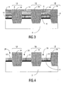
- the sacrificial layer 8, first floating gate layer 6, tunnel insulating layer 4 and a trench 10 in the substrate 2 are etched in subsequent etching steps. The result after this etch, and after removal of any remaining parts of the mask, if present, is shown in Fig. 2 .
- First portions 12 of the floating gate have been formed, on top of which caps 14 formed out of the sacrificial layer 8 are present. If the mask has disappeared during the subsequent etching steps, the sacrificial layer 8 functions as a hard mask. It is possible to provide a mask having a thickness sufficient to only etch the sacrificial layer 8. After etching of the sacrificial layer 8, the mask may be removed, i.e. e.g. remaining resist may be stripped before carrying out a subsequent etching step.
- the floating gates are self-aligned with the active region, no slits have to be etched to separate adjacent floating gates and therefore the width of the STI trench 10 can be small.
- the associated increased active width increases the read-current of the transistor.
- a liner oxidation is carried out to repair the damage caused by the trench etch. This may be done by carrying out a heat treatment in a nitrogen atmosphere followed by a thermal oxidation.
- This oxidation step forms an isolation trench covering film (not represented), e.g. consisting of silicon oxide at the inner walls of the trench 10. It is to be noted that, at the time of the oxidation step, both the substrate 2 and the free surfaces of the first portions 12 of the floating gate are oxidized.
- the trench 10 is filled with insulating material 16 such as oxide (e.g. TEOS or HDP oxide).
- oxide e.g. TEOS or HDP oxide
- This insulating layer 16 may be a silicon oxide layer which is deposited, for example by a low pressure chemical vapor deposition (LPCVD) procedure or by a plasma enhanced chemical vapor deposition (PECVD) procedure, in a thickness between about 300 and 1500 nm.
- LPCVD low pressure chemical vapor deposition
- PECVD plasma enhanced chemical vapor deposition
- silicon oxide, from regions other than the inside of the shallow trenches 10, thus down to the top level of the caps 14 formed by the sacrificial layer 8, is accomplished using either a chemical mechanical polishing (CMP) procedure or similar process (wherein the caps 14 formed by the sacrificial layer 8 are used as a stop layer for CMP), or via a RIE procedure using a suitable etchant or similar substance, resulting in insulator filled STI regions 18 as shown in Fig. 3 .
- CMP chemical mechanical polishing
- the sacrificial caps 14 on top of the first portions 12 of the floating gate are removed, e.g. etched away by either a wet or a dry etching step or similar process, thus leaving cavities 20 defined by the STI 18 and the top surface of the first portion 12 of the floating gate. Also protection layer 9 is removed, as shown in Fig. 4 .
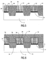
- a second layer of FG material is formed, e.g. a second layer of polysilicon is deposited.
- the second layer of FG material is preferably of the same composition as the first FG layer 6.
- the thickness of this second layer of FG material should fill the cavities 20 between the STI insulating material 16.
- This second layer of FG material is removed from regions other than the inside of the cavities 20, e.g. by polishing, more specifically by CMP for example, down to the same height as the STI insulating material 16.
- the polishing of the second layer of FG material should stop on the STI insulating material 16.
- the slurry or fixed abrasives for polysilicon-CMP should be selective towards oxide.
- the result after removal of the second layer of FG material from regions other than the inside of the cavities 20 is shown in Fig. 5 .
- the remaining parts 22 of the second layer of FG material form second portions of the floating gate, whereby the first portions 12 and the second portions 22 of the floating gate together form the floating gate 24.
- the STI insulating material 16 can be etched back, either wet or dry, but should remain above the bottom of the first portions 12 of the floating gate, as shown in Fig. 6 . This etch uncovers part of the sidewalls 26 of the FG 24.
- the uncovered part of the side walls 26 of the FG 24 may be only part of the side wall of the second portion 22 of the FG 24, or the complete side wall of the second portion 22 of the FG 24, or the complete side wall of the second portion of the FG 24 and a part of the side wall of the first portion 12 of the FG 24. Exposing more of the sidewall of the FG 24 increases the coupling between FG 24 and control gate (still to be formed), because of the capacity between FG sidewall and the control gate.
- the IPD 28 preferably comprises a plurality of insulating materials, e.g. an Oxide Nitride Oxide (ONO) layer, and may be formed or grown by conventional techniques.
- An ONO layer preferably comprises successive layers of silicon dioxide, silicon nitride and silicon dioxide. The total dielectric thickness of the ONO layer generally is between about 10 to 50 nm.
- the floating gate 24 has the same shape as in 'standard' non-volatile memories with STI, the IPD reliability is comparable, contrary to other designs to increase the coupling with 'self-aligned' STI, in which (extra) sharp corners are formed on the floating gate material, which degrades the reliability of the non-volatile cell.
- control gate material 30, e.g. polysilicon is deposited (preferably in situ doped), as shown in Fig. 6 .
- the deposition of the CG polysilicon layer 30 may be done by LPCVD procedures or similar processes, in a thickness between about 50 and 400 nm. Doping of the CG layer 30 is either accomplished in situ, during deposition, via the addition of a suitable dopant impurity such as arsine or phosphine to a silane ambient, or via an ion implantation procedure, using such a dopant, e.g. arsenic, phosphorous or boron ions applied to an intrinsically polysilicon layer.
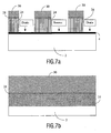
- CGs are patterned.
- the effect of the control gate mask cannot be seen in the cross section of Fig. 6 .
- the word lines are visible in a cross section perpendicular to the one in Fig. 6 , as shown in Fig. 7a and Fig. 7b .
- any reference signs placed between parentheses shall not be construed as limiting the claim.
- the word “comprising” does not exclude the presence of elements or steps other than those listed in a claim.
- the word “a” or “an” preceding an element does not exclude the presence of a plurality of such elements.
Landscapes
- Semiconductor Memories (AREA)
- Non-Volatile Memory (AREA)
- Element Separation (AREA)
Claims (7)
- Verfahren zum Herstellen einer Floating-Gate-Typ-Halbleitervorrichtung auf einem Substrat (2), welches eine Oberfläche hat, wobei das Verfahren aufweist:Bilden, auf der Substratoberfläche, eines Stapels, welcher einen isolierenden Film (4), eine erste Schicht eines Floating-Gate-Materials (6) und eine Schicht eines Opfermaterials (8) aufweist,Bilden zumindest einer Isolationszone (18) durch den Stapel hindurch und in das Substrat (2) hinein, wodurch die erste Schicht des Floating-Gate-Materials (6) eine obere Oberfläche und Seitenwände (26) hat,Entfernen des Opfermaterials (8), wodurch eine Kavität (20) zurückgelassen wird, die mittels der Isolationszonen (18) und der oberen Oberfläche der ersten Schicht des Floating-Gate-Materials (6) definiert ist, undvollständiges Füllen der Kavität (20) mit einer zweiten Schicht eines Floating-Gate-Materials (22), wodurch die erste Schicht des Floating-Gate-Materials (6) und die zweite Schicht des Floating-Gate-Materials (22) zusammen ein Floating-Gate (24) bilden,wobei das Verfahren ferner, nach dem Füllen der Kavität (20), ein teilweises Entfernen der Isolationszonen (18) aufweist, um einen Teil der Seitenwände (26) des Floating-Gates (24) freizulegen.
- Verfahren gemäß Anspruch 1, wobei die zweite Schicht des Floating-Gate-Materials (22) Seitenwände hat, wobei die Isolationszonen (18) entfernt werden, um die Seitenwände der zweiten Schicht des Floating-Gate-Materials (22) vollständig und einen Teil der Seitenwände (26) der ersten Schicht des Floating-Gate-Materials (6) freizulegen.
- Verfahren gemäß Anspruch 1 oder 2, welches ferner den Schritt eines Bildens eines Steuer-Gates (30) und eines Zwischenschicht-Dielektrikums (28) zwischen dem Floating-Gate (24) und dem Steuer-Gate (30) aufweist.
- Verfahren gemäß irgendeinem der vorherigen Ansprüche, welches ferner den Schritt eines Bildens einer Schutzschicht zwischen der ersten Schicht des Floating-Gate-Materials (6) und der Opferschicht (8) aufweist.
- Verfahren gemäß irgendeinem der vorherigen Ansprüche, wobei das Opfermaterial (8) irgendeines von einer Nitridschicht, einer Oxidschicht oder einer Silizium-Carbid-Schicht ist.
- Verfahren gemäß irgendeinem der vorherigen Ansprüche, welches ferner, nach dem Füllen der Kavität (20), ein Entfernen des Floating-Gate-Materials (22) aufweist, welches außerhalb der Kavität (20) vorliegt.
- Verfahren gemäß irgendeinem der vorherigen Ansprüche, wobei die erste Schicht des Floating-Gate-Materials (6) und die zweite Schicht des Floating-Gate-Materials (22) das gleiche Material sind.
Priority Applications (1)
| Application Number | Priority Date | Filing Date | Title |
|---|---|---|---|
| EP03769739A EP1570522B1 (de) | 2002-12-06 | 2003-10-31 | Selbstausgerichtete seichte grabenisolation mit verbessertem koppelkoeffizienten in floating-gate-bauelementen |
Applications Claiming Priority (4)
| Application Number | Priority Date | Filing Date | Title |
|---|---|---|---|
| EP02080070 | 2002-12-06 | ||
| EP02080070 | 2002-12-06 | ||
| EP03769739A EP1570522B1 (de) | 2002-12-06 | 2003-10-31 | Selbstausgerichtete seichte grabenisolation mit verbessertem koppelkoeffizienten in floating-gate-bauelementen |
| PCT/IB2003/004949 WO2004053992A2 (en) | 2002-12-06 | 2003-10-31 | Shallow trench isolation in floating gate devices |
Publications (2)
| Publication Number | Publication Date |
|---|---|
| EP1570522A2 EP1570522A2 (de) | 2005-09-07 |
| EP1570522B1 true EP1570522B1 (de) | 2012-12-12 |
Family
ID=32479745
Family Applications (1)
| Application Number | Title | Priority Date | Filing Date |
|---|---|---|---|
| EP03769739A Expired - Lifetime EP1570522B1 (de) | 2002-12-06 | 2003-10-31 | Selbstausgerichtete seichte grabenisolation mit verbessertem koppelkoeffizienten in floating-gate-bauelementen |
Country Status (8)
| Country | Link |
|---|---|
| US (2) | US7419875B2 (de) |
| EP (1) | EP1570522B1 (de) |
| JP (1) | JP2006509366A (de) |
| KR (1) | KR20050085361A (de) |
| CN (1) | CN100565884C (de) |
| AU (1) | AU2003278435A1 (de) |
| TW (1) | TWI329355B (de) |
| WO (1) | WO2004053992A2 (de) |
Families Citing this family (17)
| Publication number | Priority date | Publication date | Assignee | Title |
|---|---|---|---|---|
| KR100629356B1 (ko) * | 2004-12-23 | 2006-09-29 | 삼성전자주식회사 | 필라 패턴을 갖는 플래시메모리소자 및 그 제조방법 |
| JP4734019B2 (ja) | 2005-04-26 | 2011-07-27 | 株式会社東芝 | 半導体記憶装置及びその製造方法 |
| KR100632651B1 (ko) * | 2005-09-15 | 2006-10-11 | 주식회사 하이닉스반도체 | 플래쉬 메모리소자의 제조방법 |
| US20070181916A1 (en) * | 2006-02-07 | 2007-08-09 | Hynix Semiconductor Inc. | Method of manufacturing flash memory device |
| JP2007258510A (ja) * | 2006-03-24 | 2007-10-04 | Toshiba Corp | 半導体装置の製造方法 |
| US7998809B2 (en) * | 2006-05-15 | 2011-08-16 | Micron Technology, Inc. | Method for forming a floating gate using chemical mechanical planarization |
| US7879708B2 (en) | 2006-09-21 | 2011-02-01 | Macronix International Co. Ltd. | Apparatus and associated method for making a floating gate cell with increased overlay between the control gate and floating gate |
| TW200913169A (en) * | 2007-09-13 | 2009-03-16 | Powerchip Semiconductor Corp | Method of fabricating flash memory |
| KR20140020476A (ko) * | 2012-08-08 | 2014-02-19 | 에스케이하이닉스 주식회사 | 반도체 메모리 소자 및 이의 제조방법 |
| JP2014063551A (ja) | 2012-09-21 | 2014-04-10 | Toshiba Corp | 半導体記憶装置 |
| CN104658978A (zh) * | 2013-11-19 | 2015-05-27 | 中芯国际集成电路制造(上海)有限公司 | 快闪存储器和快闪存储器的制作方法 |
| CN104752356B (zh) * | 2013-12-25 | 2018-07-06 | 北京兆易创新科技股份有限公司 | 一种或非型闪存的浮栅的制作方法 |
| CN103904036A (zh) * | 2014-04-04 | 2014-07-02 | 武汉新芯集成电路制造有限公司 | Nor闪存的制造方法 |
| CN109417094B (zh) | 2016-07-01 | 2022-10-21 | 英特尔公司 | 自-对准栅极边缘三栅极和finFET器件 |
| KR102913835B1 (ko) * | 2020-11-12 | 2026-01-19 | 삼성전자주식회사 | 반도체 소자 |
| TWI769771B (zh) * | 2021-04-01 | 2022-07-01 | 華邦電子股份有限公司 | 半導體結構及其形成方法 |
| CN115312525B (zh) * | 2021-05-07 | 2025-06-10 | 华邦电子股份有限公司 | 半导体结构及其形成方法 |
Family Cites Families (9)
| Publication number | Priority date | Publication date | Assignee | Title |
|---|---|---|---|---|
| JPH0817948A (ja) * | 1994-06-30 | 1996-01-19 | Toshiba Corp | 半導体装置及びその製造方法 |
| US5789296A (en) * | 1996-12-05 | 1998-08-04 | Mosel Vitelic Inc. | Method for manufacturing split gate flash memory |
| US6403421B1 (en) | 1998-04-22 | 2002-06-11 | Sony Corporation | Semiconductor nonvolatile memory device and method of producing the same |
| JP4237344B2 (ja) * | 1998-09-29 | 2009-03-11 | 株式会社東芝 | 半導体装置及びその製造方法 |
| JP4131896B2 (ja) * | 2000-03-31 | 2008-08-13 | 株式会社東芝 | 不揮発性半導体記憶装置の製造方法 |
| KR100331556B1 (ko) * | 1999-10-05 | 2002-04-06 | 윤종용 | 자기 정렬된 트랜치를 갖는 플레시 메모리 및 그 제조방법 |
| KR100369236B1 (ko) * | 2000-09-16 | 2003-01-24 | 삼성전자 주식회사 | 바람직한 게이트 프로파일을 갖는 반도체 장치 및 그제조방법 |
| JP3984020B2 (ja) * | 2000-10-30 | 2007-09-26 | 株式会社東芝 | 不揮発性半導体記憶装置 |
| US6391722B1 (en) * | 2001-07-13 | 2002-05-21 | Vanguard International Semiconductor Corporation | Method of making nonvolatile memory having high capacitive coupling ratio |
-
2003
- 2003-10-31 KR KR1020057010145A patent/KR20050085361A/ko not_active Ceased
- 2003-10-31 WO PCT/IB2003/004949 patent/WO2004053992A2/en not_active Ceased
- 2003-10-31 AU AU2003278435A patent/AU2003278435A1/en not_active Abandoned
- 2003-10-31 US US10/537,518 patent/US7419875B2/en not_active Expired - Lifetime
- 2003-10-31 EP EP03769739A patent/EP1570522B1/de not_active Expired - Lifetime
- 2003-10-31 JP JP2004558873A patent/JP2006509366A/ja active Pending
- 2003-10-31 CN CNB2003801051119A patent/CN100565884C/zh not_active Expired - Fee Related
- 2003-12-03 TW TW092134034A patent/TWI329355B/zh not_active IP Right Cessation
-
2008
- 2008-07-18 US US12/175,521 patent/US7763512B2/en not_active Expired - Lifetime
Also Published As
| Publication number | Publication date |
|---|---|
| EP1570522A2 (de) | 2005-09-07 |
| US20080303076A1 (en) | 2008-12-11 |
| CN100565884C (zh) | 2009-12-02 |
| KR20050085361A (ko) | 2005-08-29 |
| TW200423376A (en) | 2004-11-01 |
| AU2003278435A1 (en) | 2004-06-30 |
| WO2004053992A3 (en) | 2004-08-26 |
| CN1720618A (zh) | 2006-01-11 |
| JP2006509366A (ja) | 2006-03-16 |
| US7419875B2 (en) | 2008-09-02 |
| TWI329355B (en) | 2010-08-21 |
| US20060118861A1 (en) | 2006-06-08 |
| AU2003278435A8 (en) | 2004-06-30 |
| WO2004053992A2 (en) | 2004-06-24 |
| US7763512B2 (en) | 2010-07-27 |
Similar Documents
| Publication | Publication Date | Title |
|---|---|---|
| US7763512B2 (en) | Shallow trench isolation in floating gate devices | |
| US6153494A (en) | Method to increase the coupling ratio of word line to floating gate by lateral coupling in stacked-gate flash | |
| US7417278B2 (en) | Method to increase coupling ratio of source to floating gate in split-gate flash | |
| US8278202B2 (en) | Conductive spacers extended floating gates | |
| US6391722B1 (en) | Method of making nonvolatile memory having high capacitive coupling ratio | |
| US20080105917A1 (en) | Split-gate memory cells and fabrication methods thereof | |
| CN111430452B (zh) | 多次可编程存储器的单元结构及其制作方法 | |
| US20020160570A1 (en) | Stacked-gate flash memory and the method of making the same | |
| US6743676B2 (en) | Method of forming a floating gate in a flash memory device | |
| US7443725B2 (en) | Floating gate isolation and method of making the same | |
| US6548353B2 (en) | Method of making nonvolatile memory device having reduced capacitance between floating gate and substrate | |
| CN211350659U (zh) | 多次可编程存储器的单元结构 | |
| US20050014333A1 (en) | Method for manufacturing a semiconductor device | |
| US7579239B2 (en) | Method for the manufacture of a non-volatile memory device and memory device thus obtained |
Legal Events
| Date | Code | Title | Description |
|---|---|---|---|
| PUAI | Public reference made under article 153(3) epc to a published international application that has entered the european phase |
Free format text: ORIGINAL CODE: 0009012 |
|
| 17P | Request for examination filed |
Effective date: 20050706 |
|
| AK | Designated contracting states |
Kind code of ref document: A2 Designated state(s): AT BE BG CH CY CZ DE DK EE ES FI FR GB GR HU IE IT LI LU MC NL PT RO SE SI SK TR |
|
| AX | Request for extension of the european patent |
Extension state: AL LT LV MK |
|
| DAX | Request for extension of the european patent (deleted) | ||
| RAP1 | Party data changed (applicant data changed or rights of an application transferred) |
Owner name: NXP B.V. |
|
| 17Q | First examination report despatched |
Effective date: 20090706 |
|
| GRAP | Despatch of communication of intention to grant a patent |
Free format text: ORIGINAL CODE: EPIDOSNIGR1 |
|
| GRAS | Grant fee paid |
Free format text: ORIGINAL CODE: EPIDOSNIGR3 |
|
| GRAA | (expected) grant |
Free format text: ORIGINAL CODE: 0009210 |
|
| AK | Designated contracting states |
Kind code of ref document: B1 Designated state(s): AT BE BG CH CY CZ DE DK EE ES FI FR GB GR HU IE IT LI LU MC NL PT RO SE SI SK TR |
|
| REG | Reference to a national code |
Ref country code: GB Ref legal event code: FG4D |
|
| REG | Reference to a national code |
Ref country code: CH Ref legal event code: EP |
|
| REG | Reference to a national code |
Ref country code: AT Ref legal event code: REF Ref document number: 588695 Country of ref document: AT Kind code of ref document: T Effective date: 20121215 |
|
| REG | Reference to a national code |
Ref country code: IE Ref legal event code: FG4D |
|
| REG | Reference to a national code |
Ref country code: DE Ref legal event code: R096 Ref document number: 60342860 Country of ref document: DE Effective date: 20130207 |
|
| PG25 | Lapsed in a contracting state [announced via postgrant information from national office to epo] |
Ref country code: SE Free format text: LAPSE BECAUSE OF FAILURE TO SUBMIT A TRANSLATION OF THE DESCRIPTION OR TO PAY THE FEE WITHIN THE PRESCRIBED TIME-LIMIT Effective date: 20121212 Ref country code: FI Free format text: LAPSE BECAUSE OF FAILURE TO SUBMIT A TRANSLATION OF THE DESCRIPTION OR TO PAY THE FEE WITHIN THE PRESCRIBED TIME-LIMIT Effective date: 20121212 Ref country code: ES Free format text: LAPSE BECAUSE OF FAILURE TO SUBMIT A TRANSLATION OF THE DESCRIPTION OR TO PAY THE FEE WITHIN THE PRESCRIBED TIME-LIMIT Effective date: 20130323 |
|
| REG | Reference to a national code |
Ref country code: NL Ref legal event code: VDEP Effective date: 20121212 |
|
| REG | Reference to a national code |
Ref country code: AT Ref legal event code: MK05 Ref document number: 588695 Country of ref document: AT Kind code of ref document: T Effective date: 20121212 |
|
| PG25 | Lapsed in a contracting state [announced via postgrant information from national office to epo] |
Ref country code: GR Free format text: LAPSE BECAUSE OF FAILURE TO SUBMIT A TRANSLATION OF THE DESCRIPTION OR TO PAY THE FEE WITHIN THE PRESCRIBED TIME-LIMIT Effective date: 20130313 Ref country code: SI Free format text: LAPSE BECAUSE OF FAILURE TO SUBMIT A TRANSLATION OF THE DESCRIPTION OR TO PAY THE FEE WITHIN THE PRESCRIBED TIME-LIMIT Effective date: 20121212 |
|
| PG25 | Lapsed in a contracting state [announced via postgrant information from national office to epo] |
Ref country code: SK Free format text: LAPSE BECAUSE OF FAILURE TO SUBMIT A TRANSLATION OF THE DESCRIPTION OR TO PAY THE FEE WITHIN THE PRESCRIBED TIME-LIMIT Effective date: 20121212 Ref country code: CZ Free format text: LAPSE BECAUSE OF FAILURE TO SUBMIT A TRANSLATION OF THE DESCRIPTION OR TO PAY THE FEE WITHIN THE PRESCRIBED TIME-LIMIT Effective date: 20121212 Ref country code: BG Free format text: LAPSE BECAUSE OF FAILURE TO SUBMIT A TRANSLATION OF THE DESCRIPTION OR TO PAY THE FEE WITHIN THE PRESCRIBED TIME-LIMIT Effective date: 20130312 Ref country code: EE Free format text: LAPSE BECAUSE OF FAILURE TO SUBMIT A TRANSLATION OF THE DESCRIPTION OR TO PAY THE FEE WITHIN THE PRESCRIBED TIME-LIMIT Effective date: 20121212 Ref country code: CY Free format text: LAPSE BECAUSE OF FAILURE TO SUBMIT A TRANSLATION OF THE DESCRIPTION OR TO PAY THE FEE WITHIN THE PRESCRIBED TIME-LIMIT Effective date: 20121212 Ref country code: BE Free format text: LAPSE BECAUSE OF FAILURE TO SUBMIT A TRANSLATION OF THE DESCRIPTION OR TO PAY THE FEE WITHIN THE PRESCRIBED TIME-LIMIT Effective date: 20121212 Ref country code: AT Free format text: LAPSE BECAUSE OF FAILURE TO SUBMIT A TRANSLATION OF THE DESCRIPTION OR TO PAY THE FEE WITHIN THE PRESCRIBED TIME-LIMIT Effective date: 20121212 |
|
| PG25 | Lapsed in a contracting state [announced via postgrant information from national office to epo] |
Ref country code: NL Free format text: LAPSE BECAUSE OF FAILURE TO SUBMIT A TRANSLATION OF THE DESCRIPTION OR TO PAY THE FEE WITHIN THE PRESCRIBED TIME-LIMIT Effective date: 20121212 Ref country code: RO Free format text: LAPSE BECAUSE OF FAILURE TO SUBMIT A TRANSLATION OF THE DESCRIPTION OR TO PAY THE FEE WITHIN THE PRESCRIBED TIME-LIMIT Effective date: 20121212 Ref country code: PT Free format text: LAPSE BECAUSE OF FAILURE TO SUBMIT A TRANSLATION OF THE DESCRIPTION OR TO PAY THE FEE WITHIN THE PRESCRIBED TIME-LIMIT Effective date: 20130412 |
|
| PLBE | No opposition filed within time limit |
Free format text: ORIGINAL CODE: 0009261 |
|
| STAA | Information on the status of an ep patent application or granted ep patent |
Free format text: STATUS: NO OPPOSITION FILED WITHIN TIME LIMIT |
|
| PG25 | Lapsed in a contracting state [announced via postgrant information from national office to epo] |
Ref country code: DK Free format text: LAPSE BECAUSE OF FAILURE TO SUBMIT A TRANSLATION OF THE DESCRIPTION OR TO PAY THE FEE WITHIN THE PRESCRIBED TIME-LIMIT Effective date: 20121212 |
|
| 26N | No opposition filed |
Effective date: 20130913 |
|
| PG25 | Lapsed in a contracting state [announced via postgrant information from national office to epo] |
Ref country code: IT Free format text: LAPSE BECAUSE OF FAILURE TO SUBMIT A TRANSLATION OF THE DESCRIPTION OR TO PAY THE FEE WITHIN THE PRESCRIBED TIME-LIMIT Effective date: 20121212 |
|
| REG | Reference to a national code |
Ref country code: DE Ref legal event code: R097 Ref document number: 60342860 Country of ref document: DE Effective date: 20130913 |
|
| PG25 | Lapsed in a contracting state [announced via postgrant information from national office to epo] |
Ref country code: MC Free format text: LAPSE BECAUSE OF FAILURE TO SUBMIT A TRANSLATION OF THE DESCRIPTION OR TO PAY THE FEE WITHIN THE PRESCRIBED TIME-LIMIT Effective date: 20121212 |
|
| REG | Reference to a national code |
Ref country code: CH Ref legal event code: PL |
|
| REG | Reference to a national code |
Ref country code: IE Ref legal event code: MM4A |
|
| PG25 | Lapsed in a contracting state [announced via postgrant information from national office to epo] |
Ref country code: CH Free format text: LAPSE BECAUSE OF NON-PAYMENT OF DUE FEES Effective date: 20131031 Ref country code: LI Free format text: LAPSE BECAUSE OF NON-PAYMENT OF DUE FEES Effective date: 20131031 |
|
| PG25 | Lapsed in a contracting state [announced via postgrant information from national office to epo] |
Ref country code: IE Free format text: LAPSE BECAUSE OF NON-PAYMENT OF DUE FEES Effective date: 20131031 |
|
| PGFP | Annual fee paid to national office [announced via postgrant information from national office to epo] |
Ref country code: GB Payment date: 20140924 Year of fee payment: 12 |
|
| PGFP | Annual fee paid to national office [announced via postgrant information from national office to epo] |
Ref country code: DE Payment date: 20140924 Year of fee payment: 12 Ref country code: FR Payment date: 20141021 Year of fee payment: 12 |
|
| PG25 | Lapsed in a contracting state [announced via postgrant information from national office to epo] |
Ref country code: TR Free format text: LAPSE BECAUSE OF FAILURE TO SUBMIT A TRANSLATION OF THE DESCRIPTION OR TO PAY THE FEE WITHIN THE PRESCRIBED TIME-LIMIT Effective date: 20121212 |
|
| PG25 | Lapsed in a contracting state [announced via postgrant information from national office to epo] |
Ref country code: LU Free format text: LAPSE BECAUSE OF NON-PAYMENT OF DUE FEES Effective date: 20131031 Ref country code: HU Free format text: LAPSE BECAUSE OF FAILURE TO SUBMIT A TRANSLATION OF THE DESCRIPTION OR TO PAY THE FEE WITHIN THE PRESCRIBED TIME-LIMIT; INVALID AB INITIO Effective date: 20031031 |
|
| REG | Reference to a national code |
Ref country code: DE Ref legal event code: R119 Ref document number: 60342860 Country of ref document: DE |
|
| GBPC | Gb: european patent ceased through non-payment of renewal fee |
Effective date: 20151031 |
|
| PG25 | Lapsed in a contracting state [announced via postgrant information from national office to epo] |
Ref country code: GB Free format text: LAPSE BECAUSE OF NON-PAYMENT OF DUE FEES Effective date: 20151031 Ref country code: DE Free format text: LAPSE BECAUSE OF NON-PAYMENT OF DUE FEES Effective date: 20160503 |
|
| REG | Reference to a national code |
Ref country code: FR Ref legal event code: ST Effective date: 20160630 |
|
| PG25 | Lapsed in a contracting state [announced via postgrant information from national office to epo] |
Ref country code: FR Free format text: LAPSE BECAUSE OF NON-PAYMENT OF DUE FEES Effective date: 20151102 |