EP1569260A2 - Photomultiplicateur - Google Patents
Photomultiplicateur Download PDFInfo
- Publication number
- EP1569260A2 EP1569260A2 EP05251121A EP05251121A EP1569260A2 EP 1569260 A2 EP1569260 A2 EP 1569260A2 EP 05251121 A EP05251121 A EP 05251121A EP 05251121 A EP05251121 A EP 05251121A EP 1569260 A2 EP1569260 A2 EP 1569260A2
- Authority
- EP
- European Patent Office
- Prior art keywords
- photomultiplier
- gain
- dynode
- dynodes
- modifying element
- Prior art date
- Legal status (The legal status is an assumption and is not a legal conclusion. Google has not performed a legal analysis and makes no representation as to the accuracy of the status listed.)
- Granted
Links
Images



Classifications
-
- H—ELECTRICITY
- H01—ELECTRIC ELEMENTS
- H01J—ELECTRIC DISCHARGE TUBES OR DISCHARGE LAMPS
- H01J9/00—Apparatus or processes specially adapted for the manufacture, installation, removal, maintenance of electric discharge tubes, discharge lamps, or parts thereof; Recovery of material from discharge tubes or lamps
- H01J9/02—Manufacture of electrodes or electrode systems
- H01J9/12—Manufacture of electrodes or electrode systems of photo-emissive cathodes; of secondary-emission electrodes
- H01J9/125—Manufacture of electrodes or electrode systems of photo-emissive cathodes; of secondary-emission electrodes of secondary emission electrodes
-
- H—ELECTRICITY
- H01—ELECTRIC ELEMENTS
- H01J—ELECTRIC DISCHARGE TUBES OR DISCHARGE LAMPS
- H01J43/00—Secondary-emission tubes; Electron-multiplier tubes
- H01J43/04—Electron multipliers
-
- H—ELECTRICITY
- H01—ELECTRIC ELEMENTS
- H01J—ELECTRIC DISCHARGE TUBES OR DISCHARGE LAMPS
- H01J43/00—Secondary-emission tubes; Electron-multiplier tubes
- H01J43/04—Electron multipliers
- H01J43/06—Electrode arrangements
- H01J43/18—Electrode arrangements using essentially more than one dynode
-
- H—ELECTRICITY
- H01—ELECTRIC ELEMENTS
- H01J—ELECTRIC DISCHARGE TUBES OR DISCHARGE LAMPS
- H01J9/00—Apparatus or processes specially adapted for the manufacture, installation, removal, maintenance of electric discharge tubes, discharge lamps, or parts thereof; Recovery of material from discharge tubes or lamps
- H01J9/44—Factory adjustment of completed discharge tubes or lamps to comply with desired tolerances
Definitions
- the present invention relates to a photomultiplier.
- the invention relates to a photomultiplier tube in which the gain, and therefore the overall sensitivity, may be tuned after the usual activation process.
- Photomultiplier tubes are sealed, evacuated electronic devices which detect light, usually at very low levels, and yield a current output of useable magnitude.
- Photons incident on a photocathode liberate electrons by the photoelectric effect.
- the liberated electrons are focussed and accelerated to impact on the first of a cascade of dynodes held at a more positive electrical potential than the photocathode.
- the second and subsequent dynodes are held at progressively more positive potentials.
- Each dynode is provided, during a process known as activation, with a surface that releases a number of secondary electrons per incident electron, the ratio of secondary to incident electrons (gain) increases as the electric potential between the dynodes increases.
- the secondary electron amplification process is repeated at each dynode stage, such that the number of electrons incident on a final collector held at a still more positive potential, the anode, is significantly greater than the number of electrons emitted by the photocathode, i.e. there is gain, often up to 10 6 or more.
- the gain of the device is an important parameter in practical applications, and it is often desirable to have a photomultiplier with a predetermined gain.
- One procedure outlined in GB 2 113 000, is to provide a wire, coated with antimony at an equipotential line between dynodes. This material, when combined with an alkali metal forms an appropriate emissive surface on the dynode.
- the wire is heated through radio-frequency induction which causes the evaporation of the antimony, and its deposition on the facing dynodes, where it provides one component of an emissive surface.
- the other main component of the emissive surface, an alkali metal is fired separately. The activation process is then completed and the photomultiplier tube is made ready for use.
- each individual device of a specific type will have a gain value (and so overall sensitivity) for a specific applied overall voltage which varies significantly from the mean value for photomultiplier tubes of that type, at that specific applied overall voltage.
- This variation in gain is due to variations in the activation process and ultimately to tolerance variations of the mechanical size and fit of the component parts.
- the variation in gain is of a factor in the order of 100 to 1, meaning that the gain of one photomultiplier may be one hundred times the gain of another photomultiplier manufactured using the same process, even in the same batch.
- the variation in gain is often normalised by applying appropriate different overall voltages to each device, but this is undesirable in situations in which a user intends to operate more than one photomultiplier from a single power supply. Such an approach may further be detrimental to other aspects of the performance of the photomultiplier, e.g. time response.
- Another known method to normalise gain is to maintain the overall applied voltage but to vary individual elements of the voltage divider network so as to vary the potential applied to a particular dynode within the limits of the potentials applied to the dynodes preceding and following it. In this way the gains of the various dynode stages may be altered. However, in certain practical applications, this approach is not satisfactory, since this variation of the interdynode voltages may also be detrimental to the performance of the photomultiplier in other respects.
- a photomultiplier comprising a photocathode, a plurality of dynodes, the dynodes having an emissive surface of a first material and an anode, the photomultiplier further comprising a gain modifying element of a second material disposed between successive dynodes, the second material being different from the first material.
- the element is disposed between two dynodes.
- the gain modifying element may be disposed between the photocathode and the first dynode, or anywhere else within the photomultiplier.
- the provision of the gain modifying element within the photomultiplier tube may have the advantage of enabling the modification of the gain of the dynode without adjusting the overall potential of the photomultiplier or the interdynode potentials.
- the gain can be reduced to a stable value, through appropriate choice of material coating of the wire. It is undesirable to use any of the materials which make up the original secondary emissive surface, as this material would chemically react with the surface over time, leading to unstable gain behaviour.
- the gain modifying element is a gain reducing element. Therefore, this invention provides a way to reduce the gain of the photomultiplier and involves the realisation that reduction of gain can be of use in standardising the gain
- the gain modifying element is adapted to deposit a second material on one or more dynodes, thereby altering the secondary electron emission characteristics of those dynodes, preferably after the usual activation process. Therefore this invention involves the realisation that the emissive surface may be modified after activation, advantageously by an internal element, to bring the gain closer to a desired value.
- the change in gain may be permanent or temporary.
- secondary electron emission characteristics of a dynode we mean primarily the ratio of the number of secondary electrons emitted by that dynode over the number of electrons incident on the dynode, and statements relating to the deterioration or improvement of the electron emission characteristics of a dynode mean primarily a decrease or an increase, respectively, in that ratio.
- the gain modifying element may be coated or formed from the material to be deposited, which is preferably unreactive in order to reduce the likelihood of the material reacting, for example, with the material of the electrodes, and thereby to increase the stability of the gain.
- the gain modifying element is, advantageously, internal to the photomultiplier.
- the second material may be one, such as a non-alkali metal, for example manganese or aluminium, which causes deterioration of the secondary electron emission characteritics of the dynode.
- a non-alkali metal for example manganese or aluminium
- the first material may be either a combination of antimony with an alkali metal such as caesium; or beryllium oxide or a combination.
- Coating the emissive surface of a dynode with a non-emissive material, such as a non-alkali metal is counter-intuitive, but effective, way to control gain.
- the emissive surface of the dynode may comprise a mixture and/or alloy of antimony, an alkali metal, and/or beryllium oxide.
- the gain modifying element comprises a wire, preferably located along a line of equipotential within the dynode cascade (i.e. between dynodes) of the photomultiplier.
- the electromagnetic effects of the presence of the wire may be minimised by applying to it the potential which the equipotential line would have in the absence of the wire.
- the wire is as thin as possible in order also to minimise its importance as a physical obstruction.
- wires known as "focusing wires” have been placed between dynodes in order to provide an electromagnetic effect (such as increasing the time response of the photomultiplier). In order to provide (rather than minimise) such an effect such wires have not been placed on equipotential lines, nor had their potential tied to a dynode.
- the wire is located-along-a line which, in the absence-of the wire, would have the same potential as one of the dynodes and the wire is electrically connected to that dynode. In this way, the wire is maintained at the same potential as the dynode.
- the electrical connection between the wire and the dynode is preferably wholly within an evacuated chamber of the photomultiplier. In this way, the number of pins passing through the wall of the chamber may be minimised, potentially resulting in greater ease of construction.
- the photomultiplier preferably comprises more than two (for example between 6 and 14) dynodes.
- the gain modifying element is preferably located towards the middle of the dynode cascade.
- the gain modifying element may preferably be located between the fourth and fifth dynodes, the fifth and sixth dynodes or the sixth and seventh dynodes.
- the gain modifying element may be electrically connected to a connector which preferably passes though the chamber of the photomultiplier, for example an electrically isolated pin.
- the chamber preferably is a vacuum sealed envelope.
- the gain modifying element is connected to a dynode at one end and electrically connected to one external connector at another.
- the gain modifying element is electrically connected to two external connectors.
- the external connector provides a way of activating the gain modifying element.
- the gain modifying element may thereby be connected to a current source and a current, conveniently of more than 1 A, preferably substantially 2 A, passed through it. This will heat the element sufficiently for the second material to be deposited on the emissive surface.
- the two external connectors allow the-gain modifying element to be held at a voltage other than the voltage of a dynode.
- Providing an element at an alternate voltage, preferably a more positive voltage, may attract electrons to the element, rather than allowing them to travel through the photomultiplier, thereby lowering the gain of the photomultiplier.
- a photomultiplier comprising a chamber, a photocathode, a plurality of dynodes, and an anode, the photomultiplier further comprising a gain modifying element disposed between successive dynodes and being electrically connected to a connector external to the chamber.
- the chamber comprises a vacuum sealed envelope.
- the chamber houses the photocathode the dynodes and the anode.
- the gain modifying element may be electrically connected to a second connector external to the chamber.
- a batch of photomultipliers each comprising a plurality of dynodes having an emissive surface formed of a mixture of materials the proportions of materials in the mixture being chosen such that each photomultiplier in the batch has substantially the same intrinsic gain.
- batch means a group of photomultipliers manufactured according to substantially the same process on substantially the same equipment, preferably within a time window such as a day, a week or a fortnight.
- the intrinsic gain of the photomultipliers is substantially the same to within a factor of 2 to 1, conveniently 1.5 to 1, preferably 1.25 to 1 in a preferred embodiment 1.2 to 1, even 1.1 to 1.
- a method of manufacturing a photomultiplier providing a gain modifying element (preferably in the form of a wire) between dynodes of the photomultiplier, and actuating the gain modifying element after activation of the photomultiplier.
- a gain modifying element preferably in the form of a wire
- the gain modifyingelement is located along a line of equipotential of the photomultiplier.
- the method preferably comprises the step of causing a material to be deposited (in a controllable manner) on a dynode of the photomultiplier by actuating the gain modifyingelement after activation of the photomultiplier.
- the gain modifying element is actuated by heating, preferably by passing a current through the gain modifying element.
- the method may comprise pulsing the current such that the element is heated and the material is deposited, but the dynodes and, preferably, the rest of the photomultiplier remain relatively cool. This lessens the risk of decomposition of the original emissive surface of the dynodes.
- a method of manufacturing a photomultiplier comprising vaporising a material and selectively depositing the vaporised material on one or more dynodes to adjust the gain of those dynode, the material being different from the materials making up an emissive surface of the dynodes.
- the material is vaporised within an envelope of the photomultiplier.
- the second material may be a non-alkali metal, preferably manganese or aluminium.
- the deposition of the material reduces the gain of the photomultiplier.
- a method of altering the gain of a photomultiplier in use comprising actuating a gain modifying element located between dynodes of the photomultiplier.
- the gain modifying element reduces the gain of the photomultipler when actuated.
- Actuation of the gain modifying element preferably modifies the electromagnetic field between dynodes of the photomultiplier when in use
- a potential applied to the gain modifying element may be such that electrons emitted by a a dynode of the photomultiplier do not reach a subsequent dynode of the photomultiplier.
- Photomultiplier tubes manufactured or adapted to be used as outlined above are also provided in accordance with aspects of this invention.
- FIG. 1 shows, in a simplified schematic form, a linear-focus type photomultiplier having a series of staggered opposing dynodes of part-cylindrical form.
- the photomultiplier 2 comprises an evacuated chamber 4, commonly formed of glass, which houses a photocathode 6, a plurality (for example, between six and fourteen) dynodes 8 and an anode 10.
- Light enters the chamber 4 through a window 12, also commonly formed of glass, and is incident on the photocathode 6.
- Further electrodes 14 are also included (at least in the photomultiplier shown in Figure 1), most commonly between the photocathode 6 and first dynode 8a and termed focusing electrodes.
- the focusing electrodes 14 aid electron collection and/or timing between the photocathode 6 and the first dynode stage.
- the photomultiplier is activated by evacuating the chamber 4 and coating (by deposition of alkali metal vapours) the photocathode 6 and the dynodes 8 with a material which emits photoelectrons or secondary electrons, for example an alkali metal in combination with antimony BeO or other secondary emissive material.
- the material combination is selected depending upon the frequency of radiation to which the photomultiplier is intended to be sensitive. In order to provide long-term relatively static gain at each stage, the material is also selected to minimise the likelihood that it might react with the substrate of the electrodes and cause the gain to vary.
- the tube is then sealed and a burn-in or ageing step is usually taken in which operating potentials are applied to the electrodes of the photomultiplier in order to allow any initial variations in gain to settle.
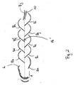
- Figure 2 shows the location of the electrodes in a particular embodiment of a photomultiplier having ten dynodes 8a to 8j. In this case, the chamber 4 is not shown.
- the photon input to the photocathode gives rise to photoelectron emission.
- the electrons emitted are attracted to a first dynode 8a which is held at a positive voltage with respect to the photocathode.
- the first dynode 8a has a prepared surface that will in turn give rise to secondary electron emission due to the impact of the incident primary photoelectrons. More output secondary electrons can be produced than input primaries, so gain occurs. This gain is dependent on the surface coating of the dynode (which may comprise, for example, antimony and an alkali metal; e.g. caesium, or BeO or both; or other secondary emissive material or combination), the impact energy of the input electrons (which is a function of the applied voltage), and the incident angle of the input electrons.
- the dynode which may comprise, for example, antimony and an alkali metal; e.g. caesium, or BeO or both; or other secondary emiss
- the output secondary electrons from the last dynode 8j are collected by the anode 10, which provides the photomultiplier output signal (current).
- the overall gain produced by the dynode cascades of typical photomultipliers may be up to 10 6 or more.
- the photocathode 6 is held at 0v
- the first dynode 8a is held at +150v
- subsequent dynodes are held 75v more positive than the preceding dynode (i.e. the second dynode 8b is at +225v
- the third dynode 8c is at +300v, etc)
- the anode 10 is held 75v more positive than the final dynode 8j (i.e. +900v).
- the photomultiplier 2 further comprises, or is connected to, a voltage divider network (not shown) comprising, for example, a series of high value resistors. Tappings of the voltage divider network provide the progressively higher (positive) voltages to the photocathode 6, the cascade of dynodes 8, and the anode 10 of the photomultiplier 2.
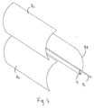
- the photomultiplier shown in Figure 1 further comprises a gain modifying element in the form of a wire 16 disposed between two dynodes 8c, 8d.
- the wire 16 extends in a direction parallel to the surfaces of the part-cylindrical dynodes 8c, 8d, which is a line of equipotential of the photomultiplier.
- the photomultiplier shown in Figure 2 also comprises a gain modifying element in the form of a wire in the location denoted 16', between dynodes 8e and 8f.
- One or more of the electrically isolated pins may be electrically connected to either one, or both, ends of the gain modifying element.
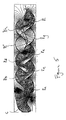
- Figure 3 shows the photocathode 6, the dynodes 8, the anode 10 and the wire 16 of the photomultiplier shown in Figure 2. Also shown are lines indicating the locations of surfaces of equipotential between the electrodes when they are held at their operating potentials.
- the wire 16 is aligned such that it is parallel to the surfaces of the part-cylindrical dynodes. It thus occupies a straight line within a plane of equipotential (when the photomultiplier is in use). In this position, by applying the appropriate potential to the wire (in fact in this embodiment, the same potential as dynode 8f), it is possible to hold the wire at the same potential as the electric field would be at the wire's position were the wire absent.
- the wire has little or no modifying effect on the electric field pattern when the photomultiplier is in use.
- This is illustrated by the symmetry of the distribution of equipotentials between the fifth and sixth dynodes 8e, 8f (where the wire 16 is located) and, for example, between the third and fourth dynodes 8c, 8d and between the eighth and ninth dynodes 8g, 8h.
- a wire which is thin in comparison with the distance between dynodes it is possible to reduce the importance of the wire as a physical obstruction to electrons passing between dynodes.
- the wire 16 is coated with a material, preferably a metal, and is actuated by heating after the usual activation stage of the manufacture of the photomultiplier (described above) such that the metal is deposited on the surface of one or more dynodes (e.g. 8e and 8f).
- a material preferably a metal
- the material for example, a non-alkali metal such as manganese or aiuminium
- the material is selected for the property that it reduces the secondary emission characteristics of the-surface of the-dynode or dynodes onto which it is deposited, thereby reducing the gain at that dynode or dynodes to a desired level.
- the wire 16 is again coated with a material and heated at a stage after the usual activation stage of the manufacture of the photomultiplier such that the metal is deposited on the surface of one or more dynodes (e.g. 8e and 8f).
- the metal for example, an alkali metal
- the metal is selected for the property that it increases the secondary emission characteristics of the surface of the dynode or dynodes onto which it is deposited, thereby increasing the gain at that dynode or dynodes to a desired level.
- the modification of secondary emission characteristics in the above two embodiments, and hence the placement of the wire or wires, is carried out at a dynode stage part way along the cascade of dynodes (for example between the fifth and sixth dynodes 8e, 8f of a photomultiplier having ten dynodes, such as that shown, between the n-5 and n-4 dynode of a photomultiplier having n dynodes, where n is, for example, 10, 11, 12, 13 or 14), rather than in the early dynode stages, close to the photocathode 6 (which might result in increased noise-in-signal), or in the end stages, close to the anode 10 (which might be detrimental to pulse height linearity).
- the gain modifying element in both of the above embodiments is electrically connected at one end to an adjacent dynode and at its other end to one of the electrically isolated pins. It is thus held at the voltage of the adjacent dynode.
- the pin to which it is electrically connected is connected to a current source such that a current of substantially 2 amps flows in the gain modifying element. This causes the gain modifying element to heat up and emit gain modifying material.
- the voltage of the current source is controlled so that the current through the gain modifying element is pulsed. The current passed in a pulse is sufficient to heat up the gain modifying element, but insufficient to heat other elements of the photomultiplier.
- the number of pulses is controlled such that a desired quantity of material is deposited on the emissive surface.
- the gain (or the sensitivity) of the photomultiplier may be measured between pulses.
- the pattern of electric field intensity between electrodes of a photomultiplier tube is important for the efficient transfer of electrons from one dynode to the next. Any modification of the pattern of those fields from the optimum could bring about a corresponding disruption of the electrons' paths from one dynode to the next.
- the potential of the wire 16 is controlled during operation of the photomultiplier.
- the potential is the result of the effects of at least three dynodes at different potentials.
- the wire is located along an equipotential at which the potential is the same as that of one of the three closest dynodes. In such a position it is well-placed to deposit the metal onto at least one of them.
- the wire 16 is connected by a connection 18 to the dynode 8d having the same potential as the position of the wire 16 would have in the absence thereof, so that the wire has the above-described lack of modifying effect on the electric field pattern when the photomultiplier is in use.
- the electrical connection to the wire (for passing a current therethrough when gain tuning is to be performed) is made internally in common with the connection to the relevant dynode. The other end of the wire passes through a wall of the chamber 4.
- the wire 16 should at no time during operation of the photomultiplier be left completely unconnected (or "floating") as such a condition would cause erratic operation of the photomultiplier. Instead, the wire is attached to a tapping of the voltage divider network (not shown) which powers the photomultiplier, which tapping is at the desired potential for the wire.
- the embodiment described above is manufactured in a known manner, with the additional step of providing one or more gain-modifying wires 16 in one or more positions as described above.
- the procedure for the gain tuning of a photomultiplier comprises the passing of a current through the gain-modifying wire (or wires) to induce the deposition of the metal coated thereon onto the dynode (or dynodes).
- the necessary duration and current are dependent upon the desired modification of gain, the materials being used and the physical characteristics of the photomultiplier and may be determined experimentally.
- the gain tuning step may be taken while the photomultiplier tube is attached to a vacuum processing station by which it is evacuated, after the usual activation process.
- the manufacturing process includes a "burn in” or “aging” step, and the gain tuning step is performed after this process.
- the burn in step is repeated after the gain tuning procedure and/or the photomultiplier is tested.
- the heating of the gain-modifying wire (or wires) 16 is achieved by alternative methods, such as RF heating (also known as eddy current heating B "ECH").
- RF heating also known as eddy current heating B "ECH”
- ECH eddy current heating B
- the gain-modifying wire 16 may be used additionally or alternatively to modify the gain of the photomultiplier during operation thereof, without modifying the overall potential of the photomultiplier, or its interdynode potentials. This may be achieved by using deliberately modifying the electric field patterns-between the dynodes during operation of-the-photomultiplier, essentially by passing a current through the gain-modifying wire (or wires) 16. Since the electric field between two dynodes controls the flow of electrons from one to the next, deliberate modification of that field may be used to reduce the number of electrons emitted by one dynode arriving at the next dynode.
- Figure 5 shows the main electrodes of the photomultiplier shown in Figures 2 and 3 and the equipotentials with the electrodes held at the potentials set out above.
- the wire 16 instead of +525V (the potential of the adjacent dynode 8f) the wire 16 is held at +650V, i.e. it is positive compared with the dynodes surrounding it.
- Statistically predicted electron paths are also shown in this Figure.
- the gain-modifying wire 16 may be used to reduce the gain of the photomultiplier to near zero (by applying a large positive potential, whereupon the gain-modifying wire will pre-emptively collect the electrons passing it). In this way, the activity of the photomultiplier tube is effectively "switched off' at required times, or, more commonly, is repeatedly switched "off-and-on” at some, often rapid, desired rate.
- Figure 6 shows a similar arrangement in which the wire 16 is held at 0V (that is the same potential as the cathode). Since the wire is then significantly negative compared with the surrounding dynodes (e.g. 8e, 8f), it modifies the electric field between the dynodes such that electrons emitted by the fifth dynode 8e do not reach the sixth dynode 8f, but instead return to the fifth or fourth dynodes 8e, 8d.
- the wire 16 is held at 0V (that is the same potential as the cathode). Since the wire is then significantly negative compared with the surrounding dynodes (e.g. 8e, 8f), it modifies the electric field between the dynodes such that electrons emitted by the fifth dynode 8e do not reach the sixth dynode 8f, but instead return to the fifth or fourth dynodes 8e, 8d.
- the wire 16 and hence the modification of the electric field pattern is carried out at a dynode stage closer to the beginning of the cascade of dynodes, since at such locations, the cloud of electrons is smaller than at later dynode stages, where it is larger (due to the gain of the preceding dynode stages) and where the larger charge to be switched might adversely affect the faster switching speed which is an advantage of this method of gating.
- the gain-modifying wire 16 is to be used additionally or alternatively to modify the gain of the photomultiplier (but not solely to provide a gating function) during operation thereof, the gain-modifying wire is located partway along the cascade of dynodes, since it might otherwise prevent the cloud of electrons from homogenising with respect to photon events at the photocathode (if positioned too close to the photocathode) or it might degrade the pulse-height linearity (if positioned too close to the anode).
- the gain-modifying wire is electrically connected to two electrically isolated pins which pass through the vacuum sealed envelope of the photomultiplier.
- the potential required to achieve the desired modification of the gain of a multiplier is dependent upon a number of factors (particularly photomultiplier characteristics) and it may be determined experimentally.
- embodiments having only a single wire 16 have been discussed, embodiments having two or more wires may equally be provided, each wire having the same function as the single wire of the embodiments described above. Alternatively, one or more wires could be provided for increasing gain, and one or more further wires provided for reducing gain. One or more of such wires could have both functions.
- part-cylindrical in relation to the shapes of the dynodes, is intended a shape obtainable by taking a longitudinal slice of a cylinder (whether or not having a circular cross-section).
- planar dynodes, part-spheroidal dynodes or even more irregularly curved dynodes may also be used.
- a photomultiplier having an element for modifying the gain thereof either during manufacture (after the normal activation process) or in use, by changing the secondary electron emission characteristics of dynodes of the photomultiplier and/or by modifying the electromagnetic field within the photomultiplier.
- the gain modifying element is made of a different material to the emissive surface of the dynodes, and may reduce the gain of the photomultiplier.
Landscapes
- Engineering & Computer Science (AREA)
- Manufacturing & Machinery (AREA)
- Photometry And Measurement Of Optical Pulse Characteristics (AREA)
- Common Detailed Techniques For Electron Tubes Or Discharge Tubes (AREA)
- Measurement Of Radiation (AREA)
- Nuclear Medicine (AREA)
Applications Claiming Priority (2)
| Application Number | Priority Date | Filing Date | Title |
|---|---|---|---|
| GB0404282 | 2004-02-26 | ||
| GB0404282A GB2412231B (en) | 2004-02-26 | 2004-02-26 | Photomultiplier |
Publications (3)
| Publication Number | Publication Date |
|---|---|
| EP1569260A2 true EP1569260A2 (fr) | 2005-08-31 |
| EP1569260A3 EP1569260A3 (fr) | 2007-05-02 |
| EP1569260B1 EP1569260B1 (fr) | 2014-11-26 |
Family
ID=32050920
Family Applications (1)
| Application Number | Title | Priority Date | Filing Date |
|---|---|---|---|
| EP05251121.9A Expired - Lifetime EP1569260B1 (fr) | 2004-02-26 | 2005-02-25 | Photomultiplicateur |
Country Status (3)
| Country | Link |
|---|---|
| US (1) | US7592746B2 (fr) |
| EP (1) | EP1569260B1 (fr) |
| GB (1) | GB2412231B (fr) |
Families Citing this family (4)
| Publication number | Priority date | Publication date | Assignee | Title |
|---|---|---|---|---|
| US7446327B2 (en) * | 2005-04-21 | 2008-11-04 | Etp Electron Multipliers Pty Ltd. | Apparatus for amplifying a stream of charged particles |
| US10453660B2 (en) * | 2016-01-29 | 2019-10-22 | Shenzhen Genorivision Technology Co., Ltd. | Photomultiplier and methods of making it |
| KR20200094130A (ko) * | 2017-10-09 | 2020-08-06 | 아답타스 솔루션즈 피티와이 엘티디 | 다이노드 전자 방출 표면 위의 오염물 부착을 억제하는 방법 및 장치 |
| US11361951B2 (en) | 2019-10-03 | 2022-06-14 | Kla Corporation | System and method for photomultiplier tube image correction |
Family Cites Families (14)
| Publication number | Priority date | Publication date | Assignee | Title |
|---|---|---|---|---|
| FR1553045A (fr) * | 1967-11-28 | 1969-01-10 | ||
| US3753023A (en) * | 1971-12-03 | 1973-08-14 | Rca Corp | Electron emissive device incorporating a secondary electron emitting material of antimony activated with potassium and cesium |
| US4347458A (en) * | 1980-03-26 | 1982-08-31 | Rca Corporation | Photomultiplier tube having a gain modifying Nichrome dynode |
| US4341427A (en) * | 1980-06-30 | 1982-07-27 | Rca Corporation | Method for stabilizing the anode sensitivity of a photomultiplier tube |
| GB2113000A (en) * | 1981-12-05 | 1983-07-27 | Emi Ltd | Improvements relating to fast focussed electron multiplier tubes |
| US5077504A (en) * | 1990-11-19 | 1991-12-31 | Burle Technologies, Inc. | Multiple section photomultiplier tube |
| US5196690A (en) * | 1991-06-18 | 1993-03-23 | The United States Of America As Represented By The Secretary Of The Navy | Optically powered photomultiplier tube |
| JP3267644B2 (ja) * | 1991-10-24 | 2002-03-18 | 浜松ホトニクス株式会社 | 光電子増倍管 |
| US5453610A (en) * | 1994-05-20 | 1995-09-26 | Summit World Trade Corporation | Electronic gain control for photomultiplier used in gamma camera |
| JP3434574B2 (ja) * | 1994-06-06 | 2003-08-11 | 浜松ホトニクス株式会社 | 電子増倍管 |
| FR2733629B1 (fr) * | 1995-04-26 | 1997-07-18 | Philips Photonique | Multiplicateur d'electrons pour tube photomultiplicateur a plusieurs voies |
| US6384519B1 (en) * | 1996-10-30 | 2002-05-07 | Nanosciences Corporation | Micro-dynode integrated electron multiplier |
| GB2369720B (en) * | 2000-12-01 | 2005-02-16 | Electron Tubes Ltd | Photomultiplier |
| US7109463B2 (en) * | 2002-07-29 | 2006-09-19 | Applied Materials, Inc. | Amplifier circuit with a switching device to provide a wide dynamic output range |
-
2004
- 2004-02-26 GB GB0404282A patent/GB2412231B/en not_active Expired - Fee Related
-
2005
- 2005-02-25 EP EP05251121.9A patent/EP1569260B1/fr not_active Expired - Lifetime
- 2005-02-28 US US11/067,844 patent/US7592746B2/en not_active Expired - Lifetime
Non-Patent Citations (1)
| Title |
|---|
| None |
Also Published As
| Publication number | Publication date |
|---|---|
| GB2412231B (en) | 2008-09-24 |
| EP1569260A3 (fr) | 2007-05-02 |
| GB2412231A (en) | 2005-09-21 |
| GB0404282D0 (en) | 2004-03-31 |
| EP1569260B1 (fr) | 2014-11-26 |
| US20050253512A1 (en) | 2005-11-17 |
| US7592746B2 (en) | 2009-09-22 |
Similar Documents
| Publication | Publication Date | Title |
|---|---|---|
| US7141785B2 (en) | Ion detector | |
| US7855493B2 (en) | Microchannel plate devices with multiple emissive layers | |
| CN110416056B (zh) | 一种基于微通道板的高增益混合型光电倍增管 | |
| US3114044A (en) | Electron multiplier isolating electrode structure | |
| US6906318B2 (en) | Ion detector | |
| US9177764B1 (en) | Image intensifier having an ion barrier with conductive material and method for making the same | |
| US5949063A (en) | Night vision device having improved automatic brightness control and bright-source protection, improved power supply for such a night vision device, and method of its operation | |
| EP1569260B1 (fr) | Photomultiplicateur | |
| US5359187A (en) | Microchannel plate with coated output electrode to reduce spurious discharges | |
| JPS5841622B2 (ja) | 電子放電管 | |
| WO1999005697A1 (fr) | Dispositif de vision nocturne a reglage automatique de luminositeameliore | |
| US6320180B1 (en) | Method and system for enhanced vision employing an improved image intensifier and gated power supply | |
| US4446401A (en) | Photomultiplier tube having improved count-rate stability | |
| US6087649A (en) | Night vision device having an image intensifier tube, microchannel plate and power supply for such an image intensifier tube, and method | |
| Dhawan | Introduction to microchannel plate photomultipliers | |
| EP0933799B1 (fr) | Source d'électrons à photocathode avec une grille d'extraction | |
| US2227095A (en) | Discharge tube | |
| CA2457516C (fr) | Detecteur pour spectrometre de masse | |
| JP2007520048A (ja) | イオンフィードバックを抑制した平行板型電子増倍管 | |
| Sternglass et al. | Transmission secondary electron multiplication for high-speed pulse counting | |
| Yi et al. | Characteristic features of new electron-multiplying channels in a field emission display | |
| AU2226500A (en) | High energy x-ray tube | |
| CN120600616A (zh) | 一种提高空间分辨率的微通道板 | |
| JPS5812977B2 (ja) | イメ−ジカン | |
| Mansell et al. | The metal-dynode multiplier: a new component in CRT design |
Legal Events
| Date | Code | Title | Description |
|---|---|---|---|
| PUAI | Public reference made under article 153(3) epc to a published international application that has entered the european phase |
Free format text: ORIGINAL CODE: 0009012 |
|
| AK | Designated contracting states |
Kind code of ref document: A2 Designated state(s): AT BE BG CH CY CZ DE DK EE ES FI FR GB GR HU IE IS IT LI LT LU MC NL PL PT RO SE SI SK TR |
|
| AX | Request for extension of the european patent |
Extension state: AL BA HR LV MK YU |
|
| PUAL | Search report despatched |
Free format text: ORIGINAL CODE: 0009013 |
|
| AK | Designated contracting states |
Kind code of ref document: A3 Designated state(s): AT BE BG CH CY CZ DE DK EE ES FI FR GB GR HU IE IS IT LI LT LU MC NL PL PT RO SE SI SK TR |
|
| AX | Request for extension of the european patent |
Extension state: AL BA HR LV MK YU |
|
| RIC1 | Information provided on ipc code assigned before grant |
Ipc: H01J 43/18 20060101ALI20070328BHEP Ipc: H01J 43/04 20060101AFI20050616BHEP Ipc: H01J 9/12 20060101ALI20070328BHEP |
|
| 17P | Request for examination filed |
Effective date: 20071102 |
|
| AKX | Designation fees paid |
Designated state(s): AT BE BG CH CY CZ DE DK EE ES FI FR GB GR HU IE IS IT LI LT LU MC NL PL PT RO SE SI SK TR |
|
| RAP1 | Party data changed (applicant data changed or rights of an application transferred) |
Owner name: ET ENTERPRISES LIMITED |
|
| 17Q | First examination report despatched |
Effective date: 20111121 |
|
| GRAP | Despatch of communication of intention to grant a patent |
Free format text: ORIGINAL CODE: EPIDOSNIGR1 |
|
| INTG | Intention to grant announced |
Effective date: 20140624 |
|
| GRAS | Grant fee paid |
Free format text: ORIGINAL CODE: EPIDOSNIGR3 |
|
| GRAA | (expected) grant |
Free format text: ORIGINAL CODE: 0009210 |
|
| AK | Designated contracting states |
Kind code of ref document: B1 Designated state(s): AT BE BG CH CY CZ DE DK EE ES FI FR GB GR HU IE IS IT LI LT LU MC NL PL PT RO SE SI SK TR |
|
| REG | Reference to a national code |
Ref country code: GB Ref legal event code: FG4D |
|
| REG | Reference to a national code |
Ref country code: CH Ref legal event code: EP |
|
| REG | Reference to a national code |
Ref country code: AT Ref legal event code: REF Ref document number: 698623 Country of ref document: AT Kind code of ref document: T Effective date: 20141215 |
|
| REG | Reference to a national code |
Ref country code: IE Ref legal event code: FG4D |
|
| REG | Reference to a national code |
Ref country code: DE Ref legal event code: R096 Ref document number: 602005045261 Country of ref document: DE Effective date: 20150108 |
|
| REG | Reference to a national code |
Ref country code: NL Ref legal event code: T3 |
|
| REG | Reference to a national code |
Ref country code: AT Ref legal event code: MK05 Ref document number: 698623 Country of ref document: AT Kind code of ref document: T Effective date: 20141126 |
|
| REG | Reference to a national code |
Ref country code: LT Ref legal event code: MG4D |
|
| PG25 | Lapsed in a contracting state [announced via postgrant information from national office to epo] |
Ref country code: LT Free format text: LAPSE BECAUSE OF FAILURE TO SUBMIT A TRANSLATION OF THE DESCRIPTION OR TO PAY THE FEE WITHIN THE PRESCRIBED TIME-LIMIT Effective date: 20141126 Ref country code: IS Free format text: LAPSE BECAUSE OF FAILURE TO SUBMIT A TRANSLATION OF THE DESCRIPTION OR TO PAY THE FEE WITHIN THE PRESCRIBED TIME-LIMIT Effective date: 20150326 Ref country code: ES Free format text: LAPSE BECAUSE OF FAILURE TO SUBMIT A TRANSLATION OF THE DESCRIPTION OR TO PAY THE FEE WITHIN THE PRESCRIBED TIME-LIMIT Effective date: 20141126 Ref country code: PT Free format text: LAPSE BECAUSE OF FAILURE TO SUBMIT A TRANSLATION OF THE DESCRIPTION OR TO PAY THE FEE WITHIN THE PRESCRIBED TIME-LIMIT Effective date: 20150326 |
|
| PG25 | Lapsed in a contracting state [announced via postgrant information from national office to epo] |
Ref country code: AT Free format text: LAPSE BECAUSE OF FAILURE TO SUBMIT A TRANSLATION OF THE DESCRIPTION OR TO PAY THE FEE WITHIN THE PRESCRIBED TIME-LIMIT Effective date: 20141126 Ref country code: CY Free format text: LAPSE BECAUSE OF FAILURE TO SUBMIT A TRANSLATION OF THE DESCRIPTION OR TO PAY THE FEE WITHIN THE PRESCRIBED TIME-LIMIT Effective date: 20141126 Ref country code: GR Free format text: LAPSE BECAUSE OF FAILURE TO SUBMIT A TRANSLATION OF THE DESCRIPTION OR TO PAY THE FEE WITHIN THE PRESCRIBED TIME-LIMIT Effective date: 20150227 Ref country code: SE Free format text: LAPSE BECAUSE OF FAILURE TO SUBMIT A TRANSLATION OF THE DESCRIPTION OR TO PAY THE FEE WITHIN THE PRESCRIBED TIME-LIMIT Effective date: 20141126 |
|
| PG25 | Lapsed in a contracting state [announced via postgrant information from national office to epo] |
Ref country code: SK Free format text: LAPSE BECAUSE OF FAILURE TO SUBMIT A TRANSLATION OF THE DESCRIPTION OR TO PAY THE FEE WITHIN THE PRESCRIBED TIME-LIMIT Effective date: 20141126 Ref country code: DK Free format text: LAPSE BECAUSE OF FAILURE TO SUBMIT A TRANSLATION OF THE DESCRIPTION OR TO PAY THE FEE WITHIN THE PRESCRIBED TIME-LIMIT Effective date: 20141126 Ref country code: EE Free format text: LAPSE BECAUSE OF FAILURE TO SUBMIT A TRANSLATION OF THE DESCRIPTION OR TO PAY THE FEE WITHIN THE PRESCRIBED TIME-LIMIT Effective date: 20141126 Ref country code: CZ Free format text: LAPSE BECAUSE OF FAILURE TO SUBMIT A TRANSLATION OF THE DESCRIPTION OR TO PAY THE FEE WITHIN THE PRESCRIBED TIME-LIMIT Effective date: 20141126 Ref country code: RO Free format text: LAPSE BECAUSE OF FAILURE TO SUBMIT A TRANSLATION OF THE DESCRIPTION OR TO PAY THE FEE WITHIN THE PRESCRIBED TIME-LIMIT Effective date: 20141126 |
|
| REG | Reference to a national code |
Ref country code: DE Ref legal event code: R097 Ref document number: 602005045261 Country of ref document: DE |
|
| PG25 | Lapsed in a contracting state [announced via postgrant information from national office to epo] |
Ref country code: PL Free format text: LAPSE BECAUSE OF FAILURE TO SUBMIT A TRANSLATION OF THE DESCRIPTION OR TO PAY THE FEE WITHIN THE PRESCRIBED TIME-LIMIT Effective date: 20141126 |
|
| REG | Reference to a national code |
Ref country code: NL Ref legal event code: V1 Effective date: 20150901 |
|
| PG25 | Lapsed in a contracting state [announced via postgrant information from national office to epo] |
Ref country code: LU Free format text: LAPSE BECAUSE OF FAILURE TO SUBMIT A TRANSLATION OF THE DESCRIPTION OR TO PAY THE FEE WITHIN THE PRESCRIBED TIME-LIMIT Effective date: 20150225 Ref country code: NL Free format text: LAPSE BECAUSE OF NON-PAYMENT OF DUE FEES Effective date: 20150901 |
|
| REG | Reference to a national code |
Ref country code: CH Ref legal event code: PL |
|
| PLBE | No opposition filed within time limit |
Free format text: ORIGINAL CODE: 0009261 |
|
| STAA | Information on the status of an ep patent application or granted ep patent |
Free format text: STATUS: NO OPPOSITION FILED WITHIN TIME LIMIT |
|
| PG25 | Lapsed in a contracting state [announced via postgrant information from national office to epo] |
Ref country code: FI Free format text: LAPSE BECAUSE OF NON-PAYMENT OF DUE FEES Effective date: 20150225 Ref country code: MC Free format text: LAPSE BECAUSE OF FAILURE TO SUBMIT A TRANSLATION OF THE DESCRIPTION OR TO PAY THE FEE WITHIN THE PRESCRIBED TIME-LIMIT Effective date: 20141126 Ref country code: CH Free format text: LAPSE BECAUSE OF NON-PAYMENT OF DUE FEES Effective date: 20150228 Ref country code: LI Free format text: LAPSE BECAUSE OF NON-PAYMENT OF DUE FEES Effective date: 20150228 |
|
| 26N | No opposition filed |
Effective date: 20150827 |
|
| REG | Reference to a national code |
Ref country code: IE Ref legal event code: MM4A |
|
| PG25 | Lapsed in a contracting state [announced via postgrant information from national office to epo] |
Ref country code: IT Free format text: LAPSE BECAUSE OF FAILURE TO SUBMIT A TRANSLATION OF THE DESCRIPTION OR TO PAY THE FEE WITHIN THE PRESCRIBED TIME-LIMIT Effective date: 20141126 |
|
| PG25 | Lapsed in a contracting state [announced via postgrant information from national office to epo] |
Ref country code: IE Free format text: LAPSE BECAUSE OF NON-PAYMENT OF DUE FEES Effective date: 20150225 |
|
| REG | Reference to a national code |
Ref country code: FR Ref legal event code: PLFP Year of fee payment: 12 |
|
| PG25 | Lapsed in a contracting state [announced via postgrant information from national office to epo] |
Ref country code: SI Free format text: LAPSE BECAUSE OF FAILURE TO SUBMIT A TRANSLATION OF THE DESCRIPTION OR TO PAY THE FEE WITHIN THE PRESCRIBED TIME-LIMIT Effective date: 20141126 |
|
| REG | Reference to a national code |
Ref country code: FR Ref legal event code: PLFP Year of fee payment: 13 |
|
| PG25 | Lapsed in a contracting state [announced via postgrant information from national office to epo] |
Ref country code: HU Free format text: LAPSE BECAUSE OF FAILURE TO SUBMIT A TRANSLATION OF THE DESCRIPTION OR TO PAY THE FEE WITHIN THE PRESCRIBED TIME-LIMIT; INVALID AB INITIO Effective date: 20050225 Ref country code: BG Free format text: LAPSE BECAUSE OF FAILURE TO SUBMIT A TRANSLATION OF THE DESCRIPTION OR TO PAY THE FEE WITHIN THE PRESCRIBED TIME-LIMIT Effective date: 20141126 |
|
| PG25 | Lapsed in a contracting state [announced via postgrant information from national office to epo] |
Ref country code: TR Free format text: LAPSE BECAUSE OF FAILURE TO SUBMIT A TRANSLATION OF THE DESCRIPTION OR TO PAY THE FEE WITHIN THE PRESCRIBED TIME-LIMIT Effective date: 20141126 |
|
| PG25 | Lapsed in a contracting state [announced via postgrant information from national office to epo] |
Ref country code: BE Free format text: LAPSE BECAUSE OF FAILURE TO SUBMIT A TRANSLATION OF THE DESCRIPTION OR TO PAY THE FEE WITHIN THE PRESCRIBED TIME-LIMIT Effective date: 20141126 |
|
| REG | Reference to a national code |
Ref country code: FR Ref legal event code: PLFP Year of fee payment: 14 |
|
| PGFP | Annual fee paid to national office [announced via postgrant information from national office to epo] |
Ref country code: FR Payment date: 20210226 Year of fee payment: 17 |
|
| PGFP | Annual fee paid to national office [announced via postgrant information from national office to epo] |
Ref country code: GB Payment date: 20210225 Year of fee payment: 17 |
|
| REG | Reference to a national code |
Ref country code: DE Ref legal event code: R082 Ref document number: 602005045261 Country of ref document: DE Representative=s name: ZACCO LEGAL RECHTSANWALTSGESELLSCHAFT MBH, DE |
|
| GBPC | Gb: european patent ceased through non-payment of renewal fee |
Effective date: 20220225 |
|
| PG25 | Lapsed in a contracting state [announced via postgrant information from national office to epo] |
Ref country code: FR Free format text: LAPSE BECAUSE OF NON-PAYMENT OF DUE FEES Effective date: 20220228 |
|
| PG25 | Lapsed in a contracting state [announced via postgrant information from national office to epo] |
Ref country code: GB Free format text: LAPSE BECAUSE OF NON-PAYMENT OF DUE FEES Effective date: 20220225 |
|
| PGFP | Annual fee paid to national office [announced via postgrant information from national office to epo] |
Ref country code: DE Payment date: 20240225 Year of fee payment: 20 |
|
| REG | Reference to a national code |
Ref country code: DE Ref legal event code: R071 Ref document number: 602005045261 Country of ref document: DE |