EP1569016A1 - Zweidimensionaler photonischer kristall mit lokaler dreidimensionaler struktur - Google Patents
Zweidimensionaler photonischer kristall mit lokaler dreidimensionaler struktur Download PDFInfo
- Publication number
- EP1569016A1 EP1569016A1 EP03777321A EP03777321A EP1569016A1 EP 1569016 A1 EP1569016 A1 EP 1569016A1 EP 03777321 A EP03777321 A EP 03777321A EP 03777321 A EP03777321 A EP 03777321A EP 1569016 A1 EP1569016 A1 EP 1569016A1
- Authority
- EP
- European Patent Office
- Prior art keywords
- refractive index
- photonic crystal
- dimensional
- dimensional photonic
- index member
- Prior art date
- Legal status (The legal status is an assumption and is not a legal conclusion. Google has not performed a legal analysis and makes no representation as to the accuracy of the status listed.)
- Granted
Links
Images


Classifications
-
- G—PHYSICS
- G02—OPTICS
- G02B—OPTICAL ELEMENTS, SYSTEMS OR APPARATUS
- G02B6/00—Light guides; Structural details of arrangements comprising light guides and other optical elements, e.g. couplings
- G02B6/10—Light guides; Structural details of arrangements comprising light guides and other optical elements, e.g. couplings of the optical waveguide type
- G02B6/12—Light guides; Structural details of arrangements comprising light guides and other optical elements, e.g. couplings of the optical waveguide type of the integrated circuit kind
- G02B6/12002—Three-dimensional structures
-
- G—PHYSICS
- G02—OPTICS
- G02B—OPTICAL ELEMENTS, SYSTEMS OR APPARATUS
- G02B6/00—Light guides; Structural details of arrangements comprising light guides and other optical elements, e.g. couplings
- G02B6/10—Light guides; Structural details of arrangements comprising light guides and other optical elements, e.g. couplings of the optical waveguide type
- G02B6/12—Light guides; Structural details of arrangements comprising light guides and other optical elements, e.g. couplings of the optical waveguide type of the integrated circuit kind
- G02B6/122—Basic optical elements, e.g. light-guiding paths
- G02B6/1225—Basic optical elements, e.g. light-guiding paths comprising photonic band-gap structures or photonic lattices
-
- B—PERFORMING OPERATIONS; TRANSPORTING
- B82—NANOTECHNOLOGY
- B82Y—SPECIFIC USES OR APPLICATIONS OF NANOSTRUCTURES; MEASUREMENT OR ANALYSIS OF NANOSTRUCTURES; MANUFACTURE OR TREATMENT OF NANOSTRUCTURES
- B82Y20/00—Nanooptics, e.g. quantum optics or photonic crystals
-
- G—PHYSICS
- G02—OPTICS
- G02B—OPTICAL ELEMENTS, SYSTEMS OR APPARATUS
- G02B1/00—Optical elements characterised by the material of which they are made; Optical coatings for optical elements
- G02B1/002—Optical elements characterised by the material of which they are made; Optical coatings for optical elements made of materials engineered to provide properties not available in nature, e.g. metamaterials
- G02B1/005—Optical elements characterised by the material of which they are made; Optical coatings for optical elements made of materials engineered to provide properties not available in nature, e.g. metamaterials made of photonic crystals or photonic band gap materials
-
- G—PHYSICS
- G02—OPTICS
- G02B—OPTICAL ELEMENTS, SYSTEMS OR APPARATUS
- G02B6/00—Light guides; Structural details of arrangements comprising light guides and other optical elements, e.g. couplings
- G02B6/10—Light guides; Structural details of arrangements comprising light guides and other optical elements, e.g. couplings of the optical waveguide type
- G02B6/12—Light guides; Structural details of arrangements comprising light guides and other optical elements, e.g. couplings of the optical waveguide type of the integrated circuit kind
- G02B6/12007—Light guides; Structural details of arrangements comprising light guides and other optical elements, e.g. couplings of the optical waveguide type of the integrated circuit kind forming wavelength selective elements, e.g. multiplexer, demultiplexer
-
- G—PHYSICS
- G02—OPTICS
- G02F—OPTICAL DEVICES OR ARRANGEMENTS FOR THE CONTROL OF LIGHT BY MODIFICATION OF THE OPTICAL PROPERTIES OF THE MEDIA OF THE ELEMENTS INVOLVED THEREIN; NON-LINEAR OPTICS; FREQUENCY-CHANGING OF LIGHT; OPTICAL LOGIC ELEMENTS; OPTICAL ANALOGUE/DIGITAL CONVERTERS
- G02F2202/00—Materials and properties
- G02F2202/32—Photonic crystals
Definitions
- the present invention relates to a two-dimensional photonic crystal applicable to an optical multiplexing/demultiplexing device, or similar devices, used in wavelength division optical multiplex communication or other technologies. Particularly, it relates to a technique for efficiently sending and receiving light to and from the outside through an optical resonator provided in the device.
- a photonic crystal is a functional material having a periodic distribution of refractive index, which provides a band structure with respect to the energy of light or electromagnetic waves.
- One of its particular features is that it has an energy region (called the photonic bandgap) that forbids the propagation of light or electromagnetic waves.
- the defect level an energy level due to the defect within the photonic bandgap. This allows only a specific wavelength of light having an energy corresponding to the defect level to exist within the wavelength range corresponding to the energy levels included in the photonic bandgap.
- Forming a linear defect in the crystal provides a waveguide, and forming a point-like defect in the crystal provides a resonator.
- Photonic crystals can be classified into two-dimensional and three-dimensional crystals. Each of them has its own features and advantages. For example, two-dimensional crystals are advantageous in that they are relatively easy to manufacture.
- the Japanese Unexamined Patent Publication No. 2001-272555 discloses a two-dimensional photonic crystal with cylindrical holes periodically arranged in a triangular lattice pattern to provide a periodic distribution of refractive index, in which a linear zone devoid of the cylindrical holes is formed as a waveguide ([0025], Fig. 1) and a point defect is formed in proximity to the waveguide ([0029], Fig. 1).
- the Japanese Unexamined Patent Publication No. 2001-272555 includes the analysis of an embodiment of a point defect that is formed by increasing the diameter of the periodically arranged cylindrical holes.
- the applicant of the present invention has proposed the creation of a cluster defect by making defects of two or more pieces of modified refractive index areas adjacent to each other within a plurality of modified refractive index areas forming a periodic distribution of refractive index.
- the defects of the modified refractive index areas are formed by making the refractive index of the desired part of the modified refractive index areas different from that of the rest of the modified refractive index areas.
- a defect having a refractive index lower than that of the rest of the modified refractive index areas is called the acceptor type defect, whereas a defect having a higher refractive index is called the donor type defect.
- 2001-272555 which is created by enlarging the cylindrical hole, is an acceptor type defect, whereas a defect created by not providing the modified refractive index area is a donor type defect.
- the cluster defect and a point defect created by the absence of a single piece of modified refractive index area are generally called the "point-like defect.”
- the two-dimensional photonic crystal with a point-like defect or point like defects can be used for various purposes, a typical example of which is the optical multiplex communication.
- optical multiplex communications use the wavelength division multiplexing in which plural wavelengths of light, each carrying a different signal, propagate through a single transmission line.
- the two-dimensional photonic crystal With a waveguide accompanied by a plurality of point-like defects each having a defect level corresponding to each wavelength, the two-dimensional photonic crystal can be used as a demultiplexer for taking out a specific wavelength of light (i.e. signal) through each point-like defect from the light propagating through the waveguide, or as a multiplexer for introducing a specific wavelength of light through each point-like defect into the waveguide.
- the Japanese Unexamined Patent Publication No. 2001-272555 discloses a cone-shaped point defect functioning as an acceptor type defect ([0032], Fig. 5) and a point defect having different diameters on both sides ([0032], Fig. 6).
- the Japanese Unexamined Patent Publication No. 2001-272555 in [0039] and [0040], describes a method of creating a point-like defect by masking one face of a crystal with a photoresist, except for the area corresponding to the defect, and etching the face with a reactive ion beam.
- This method is capable of forming a point-like defect having a cylindrical shape or a similar shape that is symmetrical between the two sides, but not capable of forming a point-like defect having a conic shape or a similar shape that is asymmetrical between the two sides.
- the present invention aims to provide a two-dimensional photonic crystal having a point-like defect or point-like defects that enable the control of the front/back emission ratio of light and are easier to manufacture than conventional defects.
- the present invention provides a two-dimensional photonic crystal slab having a three-dimensional local structure, which is characterized by:
- the "refractive index member” is a member made of a material having a refractive index different from that of air.
- the two-dimensional photonic crystal slab having a three-dimensional local structure includes, as its base component, a two-dimensional photonic crystal whose body consists of a slab, or a plate member whose thickness is adequately smaller than its in-plane size, on which a plurality of areas having a refractive index different from that of the body are periodically arranged.
- the periodical arrangement of the modified refractive index areas creates a photonic bandgap, which prevents the existence of light whose energy is within the range of the bandgap. This means that any ray of light whose wavelength is within the photonic bandgap cannot pass through the body.
- the body may be made of Si, InGaAsP or other materials.
- a typical example of the modified refractive index area is a cylindrical hole disclosed in the Japanese Unexamined Patent Publication No. 2001-272555. Use of the cylindrical holes enables the body to be fabricated by a simple process of boring holes in the body. This process is easier than arranging some members in the body.
- a refractive index member made of a material having a refractive index different from that of air is mounted on the surface of the body in which the modified refractive index areas have been arranged.
- an appropriate setting of the refractive index (or material), shape, size and position of the refractive index member creates a defect level having a desired value within the photonic bandgap.
- the point at which the refractive index member is mounted becomes a point defect and functions as an optical resonator that generates a resonance of light at a desired wavelength. It is allowable to mount two or more pieces of refractive index members on the body. Mounting two or more pieces of refractive index members differing in material, shape or size, or in two or more of these attributes, will provide an optical resonator that generates resonances of light at two or more different wavelengths.
- the point defect created by the refractive index member becomes asymmetrical with respect to the plane of the two-dimensional photonic crystal; it becomes a point defect asymmetrical between the two sides.
- the ratio of the emission intensity of the light emitted to one side to that of the light emitted to the other side, i.e. the front/back emission ratio, can be controlled by changing the material, shape and/or size of the refractive index member.
- Changing the shape of the refractive index member enables the control of not only the front/back emission ratio of light but also the emitting direction, the degree of convergence/spread and other attributes of light.
- forming the top of the refractive index member in a concave form will cause the emitted light to converge on a single point within the space.
- the position of the convergence point can be controlled by regulating the curvature of the top.
- a convex form of the top of the refractive index member enables the radiation angle to be controlled through the regulation of the curvature of the top.
- the refractive index members may be mounted on both sides of the body. If a refractive index member is mounted on one side and another refractive index member is mounted on the other side at a position displaced from the first refractive index member, they will function as two point-like defects differing in the front/back emission ratio. If two pieces of refractive index members are mounted on both sides of the body at the same position, the refractive index members will cooperatively function as a single point-like defect. In this case, use of two refractive index members differing in material, shape or size enables the emission intensity, direction, convergence, spread and/or other attributes of light on one side to be different from that of the other side. If it is required to control the emission intensity, direction, convergence, spread and other attributes while maintaining them identical on both sides, the requirement can be met by mounting two identical pieces of refractive index members on both sides and at the same position.
- the position of a conventional type of point-like defect has been restricted to the positions of the modified refractive index areas.
- the point-like defect created by the refractive index member according to the present invention can be located at a desired position on the body.
- the resonant wavelength of light at the point defect created by the refractive index member changes depending to the positional relation between the refractive index member and the modified refractive index areas in addition to the material type and other parameters of the refractive index member itself.
- the refractive index member and the point-like defect of the modified refractive index areas cooperatively function as a single point-like defect. If each point-like defect is composed of a different point-like defect of the modified refractive index areas and a different refractive index member, the resonant wavelength can be selected with a higher degree of freedom than in the case where either a refractive index member or a point-like defect of the modified refractive index areas is solely present.
- a plurality of point-like defects of the modified refractive index areas having different resonant wavelengths are provided within the body and a plurality of refractive index members identical in material, shape and size are arranged on the surface of the body at the positions of the point-like defects of the modified refractive index areas, respectively, it is possible to take out a ray of light having a different wavelength from each defect position approximately in the same direction and with the same degree of convergence/spread.
- the material of the refractive index member may be different from or the same as that of the body. Using the same material facilitates the bonding of the refractive index member to the body. Selecting from a set of materials different from the body material allows the resonant wavelength to vary over a wide range.
- Some materials have the nature of changing their refractive index when they receive an irradiation from a laser, an application of pressure or heat, or other external operations.
- some of the InGaAsP series, InGaAlAsP series or similar types of semiconductors change their charge density and accordingly change their refractive index when a laser beam is irradiated onto them, as a result of the band-filling effect of the quantum well.
- Using such a material to fabricate a refractive index member enables the construction of an optical resonator whose resonant wavelength can be controlled by varying the external operation.
- the two-dimensional photonic crystal functions as an optical multiplexer/demultiplexer using the refractive index member to demultiplex a predetermined wavelength of light from the light propagating through the waveguide toward the outside, or multiplex a predetermined wavelength of light from the outside into the waveguide.
- the two-dimensional photonic crystal slab having a three-dimensional local structure enables the control of the front/back emission ratio, the emitting direction, the convergence/spread and other attributes of light.
- the efficiency of taking out light from the point defect can be improved by controlling the front/back emission ratio so that the emission intensity of light becomes higher on the side where the light is taken out than on the other side. Controlling the emitting direction and/or the convergence/spread of light improves the efficiency of introducing the light from the point defect into an optical fiber or other elements located outside the crystal.
- the point defect created by using the refractive index member according to the present invention is easier to manufacture than conventional types of point-like defects manufactured by asymmetrically working the body of the two-dimensional photonic crystal itself on both sides.
- the higher degree of freedom for determining the shape and material of the refractive index member makes the control of the front/back emission ratio of light easier than in the conventional cases.
- the point defect created by using the refractive index member according to the present invention provides an easier control of the emitting direction, the convergence/spread and other attributes of light than the corresponding control available with the aforementioned symmetrical point-like defect of the modified refractive index areas.
- Fig. 1 shows an embodiment of the two-dimensional photonic crystal slab having a three-dimensional local structure according to the present invention.
- the body 11 is provided with holes 12, or modified refractive index areas, periodically arranged in a triangular lattice pattern.
- the body 11 and the holes 12 constitute the two-dimensional photonic crystal.
- a refractive index member 13 is mounted on one of the holes 12.
- the point at which the refractive index member 13 is mounted functions as an optical resonator. When light is emitted from this optical resonator, the light 191 emitted from the side on which the refractive index member 13 is mounted is stronger than the light 192 emitted from the other side.
- the modified refractive index area may be created by embedding a member made of a material having a refractive index different from that of the body 11.
- the arrangement of the holes 12 may be a square lattice pattern or some other pattern different from the triangular lattice pattern.
- the refractive index member 13 may be mounted on a point different from the holes 12, e.g. on the center of gravity of a triangle in the triangular lattice pattern.
- Fig. 2 shows an embodiment of the optical multiplexer/demultiplexer using a two-dimensional photonic crystal slab according to the present invention.
- a waveguide 14 is formed in proximity to the optical resonator (i.e. the point at which the refractive index member 13 is mounted) by providing a linear defect of the holes 12 (i.e. by forming a linear zone devoid of the holes 12).
- This provides an optical multiplexer/demultiplexer that demultiplexes a ray of light having the resonant wavelength of the optical resonator from the light propagating through the waveguide 14 and sends it through the refractive index member 13 to the outside, or multiplexes a ray of light through the refractive index member 13 into the waveguide 14.
- Figs. 3 and 4 show embodiments of two-dimensional photonic crystals and optical multiplexer/demultiplexers with a refractive index member mounted on a point-like defect of the modified refractive index areas.
- a plurality of holes 12 adjacent to each other are omitted to create a donor type cluster defect 15 (as in the upper part of Fig. 3, where the absent holes are indicated by the broken line), and a refractive index member 13 is mounted on the surface at the position of the donor type cluster defect 15 (as in the lower part of Fig. 3).
- the refractive index member 13 and the donor type cluster defect 15 cooperatively function as a single point-like defect.
- the donor type cluster defect may be different from the one shown in Fig.
- the refractive index member 13 which consists of three point defects arranged in a line.
- it may consist of three point defects adjacent to each other in a triangular pattern, or two, four or more point defects adjacent to each other. It is also allowable to mount the refractive index member 13 on an acceptor type point-like defect, as in the case of the donor type cluster defect.
- donor type cluster defect 151 having a linear form and another donor type cluster defect 152 having a triangular form are now provided in a single two-dimensional photonic crystal (as in the upper drawing of Fig. 4, where each point defect is indicated by a corresponding broken line), and identical refractive index members 131 and 132 are mounted on the two-dimensional photonic crystal at the positions of the aforementioned defects (as in the lower drawing of Fig. 4) to construct two resonators each of which generates a resonance of light at a different wavelength.
- This provides an optical multiplexer/demultiplexer that demultiplexes rays of light having the aforementioned wavelengths from the waveguide 14 and sends them through the refractive index member 131 or 132 to the outside, or multiplexes rays of light from the outside through the refractive index member into the waveguide 14.
- Fig. 5 shows an embodiment of a two-dimensional photonic crystal and an optical multiplexer/demultiplexer with two or more types of refractive index members mounted on it.
- Three types of refractive index members 133, 134 and 135 having different sizes are located in proximity to the waveguide 14.
- Each point at which each refractive index member is mounted functions as an optical resonator that generates a resonance of light at a different wavelength, and the light having that wavelength is demultiplexed from the waveguide 14 through the refractive index member to the outside or multiplexed from the outside through the refractive index member into the waveguide 14.
- a difference in material, shape or other attribute of the refractive index member also enables different wavelengths of light to be multiplexed/demultiplexed.
- Figs. 6(a) and 6(b) show examples of the shape of the refractive index member as sectional views.
- the refractive index member is a cylindrical body having a concave top, which converges the emitted light onto a single point within the space.
- the top is convex shaped and emits a ray of light whose radiation angle is determined by the curvature of the convex top.
- the concave or convex section may be formed on the top of a cylinder, a rectangular solid or a similar body.
- Figs. 7(a) and 7(b) show an embodiment of the two-dimensional photonic crystal with refractive index members mounted on both sides of the crystal body at the same position.
- refractive index members 133 and 134 having different sizes and identical concave surfaces are mounted on both sides of the body 11. This construction generates an emission of light converging onto a single point within the space on each side, with different intensities on both sides.
- identical refractive index members 133 each having a convex surface are provided on both sides of the body 11. This construction generates an emission of light converging onto a single point within the space on each side, with the same intensity on both sides.
- the point-like defect in Fig. 8(a) is a donor type cluster defect consisting of three defects arranged in a line
- the one in Fig. 8(b) includes the same donor type cluster defect with two identical pieces of refractive index members 13 5 symmetrically mounted on both sides.
- the refractive index member 135 shown in Fig. 8(b) is a cylinder made of the same material as that of the body 11, which has a radius of 0.6 a and a height of 0.6 a , where a is the interval of the holes 12. The results of the calculation are shown in Figs.
- Fig. 9(a) and 9(b) show the emission intensity of light within the y-z plane shown in Figs. 8(a) and 8(b).
- Fig. 9(a) shows that the emission of light is strong not only in the direction perpendicular to the body (i.e. in z-direction) but also in a diagonal direction (at an angle of 60 degrees from z-axis).
- Fig. 9(b) shows that the diagonal emission is suppressed while the emission in z-direction is stronger than in Fig. 9(a).
- the right side pictures in Figs. 9(a) and 9(b) also show that the diagonal emission is more suppressed in Fig. 9(b) than in Fig. 9(a).
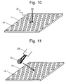
- the first manufacturing method is described with reference to Fig. 10. While a gas 21 of a material used for creating the two-dimensional photonic crystal is continuously supplied onto the surface of the crystal, a focused ion beam 22 is irradiated onto a predetermined spot so that the material is ionized and deposited to form a refractive index member.
- a focused ion beam is a type of ion beam that can be converged and irradiated onto a minimal spot of a few nanometers in diameter. This enables the refractive index member to be locally deposited.
- the ions used in the focused ion beam are Ga (gallium) ions.
- An example of the gas material is phenanthrene (C 14 H 10 ) in the case the material of the refractive index member is C (carbon).
- the second manufacturing method is described with reference to Fig. 11.
- a refractive index member 13 fabricated beforehand is mounted onto the two-dimensional photonic crystal with a nanomanipulator 23 capable of holding a member of a few nanometers in size.
- the photonic crystal and the refractive index member are bonded together by irradiating a laser beam to the boundary between them, or by other methods.
- This method allows the refractive index member 13 to be manufactured and worked outside the crystal, so that the refractive index member can be easily formed into a desired shape.
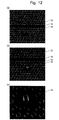
- Figs. 12(a)-12(c) show electron micrographs of a two-dimensional photonic crystal with a refractive index member formed on its surface.
- Fig. 12(a) shows a two-dimensional photonic crystal having a waveguide 14 and a linearly formed donor type cluster defect 15 before the refractive index member is formed.
- the crystal now has a refractive index member 13 made of carbon, created by the first manufacturing method.
- Fig. 12(c) provides an enlarged view of a part of the crystal shown in Fig. 12(b), including the refractive index member 13.
Landscapes
- Physics & Mathematics (AREA)
- Engineering & Computer Science (AREA)
- Optics & Photonics (AREA)
- General Physics & Mathematics (AREA)
- Microelectronics & Electronic Packaging (AREA)
- Chemical & Material Sciences (AREA)
- Nanotechnology (AREA)
- Crystallography & Structural Chemistry (AREA)
- Life Sciences & Earth Sciences (AREA)
- Biophysics (AREA)
- Optical Integrated Circuits (AREA)
Applications Claiming Priority (3)
| Application Number | Priority Date | Filing Date | Title |
|---|---|---|---|
| JP2002355631A JP3568943B2 (ja) | 2002-12-06 | 2002-12-06 | 局所的3次元構造を有する2次元フォトニック結晶スラブ |
| JP2002355631 | 2002-12-06 | ||
| PCT/JP2003/015635 WO2004053548A1 (ja) | 2002-12-06 | 2003-12-05 | 局所的3次元構造を有する2次元フォトニック結晶スラブ |
Publications (3)
| Publication Number | Publication Date |
|---|---|
| EP1569016A1 true EP1569016A1 (de) | 2005-08-31 |
| EP1569016A4 EP1569016A4 (de) | 2006-11-15 |
| EP1569016B1 EP1569016B1 (de) | 2012-08-29 |
Family
ID=32500794
Family Applications (1)
| Application Number | Title | Priority Date | Filing Date |
|---|---|---|---|
| EP03777321A Expired - Lifetime EP1569016B1 (de) | 2002-12-06 | 2003-12-05 | Zweidimensionaler photonischer kristall mit lokaler dreidimensionaler struktur |
Country Status (6)
| Country | Link |
|---|---|
| US (1) | US7397994B2 (de) |
| EP (1) | EP1569016B1 (de) |
| JP (1) | JP3568943B2 (de) |
| KR (1) | KR100962646B1 (de) |
| CN (1) | CN100363766C (de) |
| WO (1) | WO2004053548A1 (de) |
Families Citing this family (9)
| Publication number | Priority date | Publication date | Assignee | Title |
|---|---|---|---|---|
| JP4493452B2 (ja) * | 2004-09-16 | 2010-06-30 | シャープ株式会社 | 光機能素子およびその製造方法 |
| JP2006276388A (ja) * | 2005-03-29 | 2006-10-12 | Alps Electric Co Ltd | フォトニック結晶スラブ及びフォトニック結晶導波路と光デバイス |
| US7664357B2 (en) | 2006-12-07 | 2010-02-16 | Electronics And Telecommunications Research Institute | Vertical-type photonic-crystal plate and optical device assembly |
| KR100896491B1 (ko) | 2006-12-07 | 2009-05-08 | 한국전자통신연구원 | 수직형 포토닉 결정 기판 및 광 소자 어셈블리 |
| US8993993B2 (en) * | 2010-05-11 | 2015-03-31 | Samsung Electronics Co., Ltd. | Semiconductor light emitting device and method for fabricating the same |
| CN103325898B (zh) * | 2012-03-23 | 2015-11-04 | 南京理工大学 | 1.3μm波长的无偏振高效率发光量子点器件及设计方法 |
| KR102697425B1 (ko) | 2017-02-02 | 2024-08-21 | 삼성전자주식회사 | 분광기 및 그 분광기가 적용된 성분 측정 장치 |
| US11783218B2 (en) | 2018-05-10 | 2023-10-10 | The University Of British Columbia | Electromagnetic wave resonator tuning |
| CN110196469A (zh) * | 2019-06-26 | 2019-09-03 | 青岛大学 | 耦合腔光子晶体波导中的慢光特性测量及动态调制方法 |
Family Cites Families (12)
| Publication number | Priority date | Publication date | Assignee | Title |
|---|---|---|---|---|
| JPH0682642A (ja) | 1992-03-06 | 1994-03-25 | Fujitsu Ltd | 光回路デバイス、その製造方法およびそれを用いた多層光回路 |
| JP2799920B2 (ja) | 1992-06-19 | 1998-09-21 | 株式会社田村電機製作所 | 公衆電話機 |
| JPH0669490A (ja) * | 1992-08-14 | 1994-03-11 | Fujitsu Ltd | 電子光回路 |
| US6198860B1 (en) * | 1998-09-22 | 2001-03-06 | Massachusetts Institute Of Technology | Optical waveguide crossings |
| JP3925769B2 (ja) | 2000-03-24 | 2007-06-06 | 関西ティー・エル・オー株式会社 | 2次元フォトニック結晶及び合分波器 |
| JP2001281480A (ja) * | 2000-03-29 | 2001-10-10 | Nec Corp | フォトニック結晶光導波路と方向性結合器 |
| CN1156063C (zh) * | 2000-06-06 | 2004-06-30 | 中国科学院物理研究所 | 一种光子晶体微腔结构 |
| EP1305668A2 (de) * | 2000-07-31 | 2003-05-02 | Naomi Matsuura | Konfigurierbares photonisches bauelement |
| US6674949B2 (en) * | 2000-08-15 | 2004-01-06 | Corning Incorporated | Active photonic crystal waveguide device and method |
| AU2001283369A1 (en) * | 2000-08-15 | 2002-02-25 | Corning Incorporated | Active photonic crystal waveguide device |
| JP3459827B2 (ja) | 2002-03-26 | 2003-10-27 | 科学技術振興事業団 | 2次元フォトニック結晶光分合波器 |
| US6791732B2 (en) * | 2002-06-20 | 2004-09-14 | Agilent Technologies, Inc. | Systems and methods for altering the propagation of optical signals within optical media |
-
2002
- 2002-12-06 JP JP2002355631A patent/JP3568943B2/ja not_active Expired - Fee Related
-
2003
- 2003-12-05 KR KR1020057010246A patent/KR100962646B1/ko not_active Expired - Fee Related
- 2003-12-05 WO PCT/JP2003/015635 patent/WO2004053548A1/ja not_active Ceased
- 2003-12-05 US US10/537,119 patent/US7397994B2/en not_active Expired - Fee Related
- 2003-12-05 CN CNB2003801046869A patent/CN100363766C/zh not_active Expired - Fee Related
- 2003-12-05 EP EP03777321A patent/EP1569016B1/de not_active Expired - Lifetime
Also Published As
| Publication number | Publication date |
|---|---|
| US7397994B2 (en) | 2008-07-08 |
| CN100363766C (zh) | 2008-01-23 |
| CN1720471A (zh) | 2006-01-11 |
| EP1569016B1 (de) | 2012-08-29 |
| JP3568943B2 (ja) | 2004-09-22 |
| US20060051042A1 (en) | 2006-03-09 |
| WO2004053548A1 (ja) | 2004-06-24 |
| KR20050085403A (ko) | 2005-08-29 |
| JP2004191408A (ja) | 2004-07-08 |
| KR100962646B1 (ko) | 2010-06-11 |
| EP1569016A4 (de) | 2006-11-15 |
Similar Documents
| Publication | Publication Date | Title |
|---|---|---|
| US7120344B2 (en) | Two-dimensional photonic crystal cavity and channel add/drop filter | |
| US7397994B2 (en) | Two-dimensional photonic crystal slab having three-dimensional local structure | |
| CN1297829C (zh) | 二维光子晶体光复用器/解复用器 | |
| US20080219311A1 (en) | Optical structures including selectively positioned color centers, photonic chips including same, and methods of fabricating optical structures | |
| TW202017877A (zh) | 形成導角的切割方法 | |
| JP2006065273A (ja) | 3次元周期構造及びそれを有する機能素子 | |
| DE10349608B4 (de) | Optische Vorrichtung und Verfahren zum Koppeln von Ausgangslicht von einer Lichtquelle zu einem Lichtwellenleiter | |
| CN118169788A (zh) | 半导体透镜制造的优化 | |
| WO2005045492A2 (en) | Method for fabrication of optical element, and optical element having three-dimensional laminated structure | |
| WO2003081306A1 (en) | Point-defect three-dimensional photonic crystal optical resonator | |
| EP1460457A2 (de) | Hohlraumresonator eines zweidimensionalen Photonischen Kristalls und Ein-/Auskoppel-Filter für optische Kanäle | |
| US20070177644A1 (en) | Highly directional light emitting diode using photonic bandgap waveguides | |
| US9494296B2 (en) | Method of manufacturing light emitting element of fluorescent light source forming highly precise photonic structure in fluorescence emitting surface of light emitting element | |
| US7274849B2 (en) | Three-dimensional photonic crystal and functional device including the same | |
| US20070110382A1 (en) | Waveguide and device including the same | |
| CN1818798B (zh) | 在发光二极管上制作光子晶体掩膜层的方法和装置 | |
| JP7835290B2 (ja) | 光回路、量子演算装置及び光回路の製造方法 | |
| EP1785755B1 (de) | Wellenleiter und Vorrichtung damit | |
| KR102196386B1 (ko) | 레이저 다이오드, 광 집적 소자, 및 이의 제조 방법 | |
| US7820365B1 (en) | Method to fabricate a tilted logpile photonic crystal | |
| WO2025186860A1 (en) | Optical waveguide and method of manufacturing optical waveguide | |
| KR20150032087A (ko) | 금속 마스크 및 금속 마스크 제조 방법 | |
| Chanda et al. | Single laser exposure fabrication of diamond-like 3-dimensional photonic crystal microstructures using circularly polarized light | |
| KR101035557B1 (ko) | 마이크로 콜리메이터의 제조 방법 | |
| JPH01316982A (ja) | 集積型半導体レーザ装置 |
Legal Events
| Date | Code | Title | Description |
|---|---|---|---|
| PUAI | Public reference made under article 153(3) epc to a published international application that has entered the european phase |
Free format text: ORIGINAL CODE: 0009012 |
|
| 17P | Request for examination filed |
Effective date: 20050621 |
|
| AK | Designated contracting states |
Kind code of ref document: A1 Designated state(s): AT BE BG CH CY CZ DE DK EE ES FI FR GB GR HU IE IT LI LU MC NL PT RO SE SI SK TR |
|
| RBV | Designated contracting states (corrected) |
Designated state(s): DE FR GB |
|
| A4 | Supplementary search report drawn up and despatched |
Effective date: 20061012 |
|
| RTI1 | Title (correction) |
Free format text: TWO-DIMENSIONAL PHOTONIC CRYSTAL SLAB HAVING THREE-DIMENSIONAL LOCAL STRUCTURE |
|
| 17Q | First examination report despatched |
Effective date: 20101129 |
|
| REG | Reference to a national code |
Ref country code: DE Ref legal event code: R079 Ref document number: 60341968 Country of ref document: DE Free format text: PREVIOUS MAIN CLASS: G02B0006120000 Ipc: G02B0006122000 |
|
| GRAP | Despatch of communication of intention to grant a patent |
Free format text: ORIGINAL CODE: EPIDOSNIGR1 |
|
| RIC1 | Information provided on ipc code assigned before grant |
Ipc: G02B 6/12 20060101ALI20120321BHEP Ipc: G02B 6/122 20060101AFI20120321BHEP Ipc: B82Y 20/00 20110101ALI20120321BHEP |
|
| RIN1 | Information on inventor provided before grant (corrected) |
Inventor name: TANAKA, YOSHINORI Inventor name: ASANO, TAKASHI Inventor name: NODA, SUSUMU |
|
| GRAS | Grant fee paid |
Free format text: ORIGINAL CODE: EPIDOSNIGR3 |
|
| GRAA | (expected) grant |
Free format text: ORIGINAL CODE: 0009210 |
|
| AK | Designated contracting states |
Kind code of ref document: B1 Designated state(s): DE FR GB |
|
| REG | Reference to a national code |
Ref country code: GB Ref legal event code: FG4D |
|
| REG | Reference to a national code |
Ref country code: DE Ref legal event code: R096 Ref document number: 60341968 Country of ref document: DE Effective date: 20121025 |
|
| PLBE | No opposition filed within time limit |
Free format text: ORIGINAL CODE: 0009261 |
|
| STAA | Information on the status of an ep patent application or granted ep patent |
Free format text: STATUS: NO OPPOSITION FILED WITHIN TIME LIMIT |
|
| 26N | No opposition filed |
Effective date: 20130530 |
|
| REG | Reference to a national code |
Ref country code: DE Ref legal event code: R097 Ref document number: 60341968 Country of ref document: DE Effective date: 20130530 |
|
| REG | Reference to a national code |
Ref country code: DE Ref legal event code: R082 Ref document number: 60341968 Country of ref document: DE Representative=s name: HOEGER, STELLRECHT & PARTNER PATENTANWAELTE MB, DE |
|
| REG | Reference to a national code |
Ref country code: FR Ref legal event code: PLFP Year of fee payment: 13 |
|
| PGFP | Annual fee paid to national office [announced via postgrant information from national office to epo] |
Ref country code: DE Payment date: 20151111 Year of fee payment: 13 Ref country code: GB Payment date: 20151111 Year of fee payment: 13 |
|
| PGFP | Annual fee paid to national office [announced via postgrant information from national office to epo] |
Ref country code: FR Payment date: 20151113 Year of fee payment: 13 |
|
| REG | Reference to a national code |
Ref country code: DE Ref legal event code: R119 Ref document number: 60341968 Country of ref document: DE |
|
| GBPC | Gb: european patent ceased through non-payment of renewal fee |
Effective date: 20161205 |
|
| REG | Reference to a national code |
Ref country code: FR Ref legal event code: ST Effective date: 20170831 |
|
| PG25 | Lapsed in a contracting state [announced via postgrant information from national office to epo] |
Ref country code: FR Free format text: LAPSE BECAUSE OF NON-PAYMENT OF DUE FEES Effective date: 20170102 |
|
| PG25 | Lapsed in a contracting state [announced via postgrant information from national office to epo] |
Ref country code: DE Free format text: LAPSE BECAUSE OF NON-PAYMENT OF DUE FEES Effective date: 20170701 Ref country code: GB Free format text: LAPSE BECAUSE OF NON-PAYMENT OF DUE FEES Effective date: 20161205 |