EP1568151B1 - Verfahren und vorrichtung zum optimieren des wirkungsgrads eines senders - Google Patents
Verfahren und vorrichtung zum optimieren des wirkungsgrads eines senders Download PDFInfo
- Publication number
- EP1568151B1 EP1568151B1 EP03779613A EP03779613A EP1568151B1 EP 1568151 B1 EP1568151 B1 EP 1568151B1 EP 03779613 A EP03779613 A EP 03779613A EP 03779613 A EP03779613 A EP 03779613A EP 1568151 B1 EP1568151 B1 EP 1568151B1
- Authority
- EP
- European Patent Office
- Prior art keywords
- signal
- power
- peak
- control signal
- power amplifier
- Prior art date
- Legal status (The legal status is an assumption and is not a legal conclusion. Google has not performed a legal analysis and makes no representation as to the accuracy of the status listed.)
- Expired - Lifetime
Links
- 238000000034 method Methods 0.000 title claims description 23
- 238000013507 mapping Methods 0.000 claims abstract description 31
- 230000004044 response Effects 0.000 claims description 26
- 238000001914 filtration Methods 0.000 claims description 3
- 230000006870 function Effects 0.000 description 19
- 238000010586 diagram Methods 0.000 description 6
- 238000004891 communication Methods 0.000 description 4
- 238000012545 processing Methods 0.000 description 3
- 238000005457 optimization Methods 0.000 description 2
- 230000005540 biological transmission Effects 0.000 description 1
- 230000001413 cellular effect Effects 0.000 description 1
- 230000008859 change Effects 0.000 description 1
- 238000006243 chemical reaction Methods 0.000 description 1
- 238000012937 correction Methods 0.000 description 1
- 230000008878 coupling Effects 0.000 description 1
- 238000010168 coupling process Methods 0.000 description 1
- 238000005859 coupling reaction Methods 0.000 description 1
- 230000001934 delay Effects 0.000 description 1
- 230000000694 effects Effects 0.000 description 1
- 230000008569 process Effects 0.000 description 1
- 238000012360 testing method Methods 0.000 description 1
Images

Classifications
-
- H—ELECTRICITY
- H04—ELECTRIC COMMUNICATION TECHNIQUE
- H04W—WIRELESS COMMUNICATION NETWORKS
- H04W52/00—Power management, e.g. Transmission Power Control [TPC] or power classes
- H04W52/04—Transmission power control [TPC]
- H04W52/52—Transmission power control [TPC] using AGC [Automatic Gain Control] circuits or amplifiers
-
- H—ELECTRICITY
- H03—ELECTRONIC CIRCUITRY
- H03G—CONTROL OF AMPLIFICATION
- H03G3/00—Gain control in amplifiers or frequency changers
- H03G3/20—Automatic control
- H03G3/30—Automatic control in amplifiers having semiconductor devices
- H03G3/3036—Automatic control in amplifiers having semiconductor devices in high-frequency amplifiers or in frequency-changers
- H03G3/3042—Automatic control in amplifiers having semiconductor devices in high-frequency amplifiers or in frequency-changers in modulators, frequency-changers, transmitters or power amplifiers
-
- H—ELECTRICITY
- H04—ELECTRIC COMMUNICATION TECHNIQUE
- H04L—TRANSMISSION OF DIGITAL INFORMATION, e.g. TELEGRAPHIC COMMUNICATION
- H04L27/00—Modulated-carrier systems
- H04L27/26—Systems using multi-frequency codes
- H04L27/2601—Multicarrier modulation systems
- H04L27/2614—Peak power aspects
Definitions
- the present invention relates to transmitter power efficiency in communication systems and in particular to optimizing transmitter power efficiency in communication systems.
- Mobile electronic devices such as radios and cellular telephones, typically rely on power from one or more internal batteries.
- a major performance criterion for such devices is the battery life, which is typically defined as the time period for which the battery will power the device on a single charge.
- a large portion of the battery power is consumed in a power amplifier (PA) section of the mobile electronic device's transmitter.
- the power amplifier section amplifies the power of a signal to be transmitted from a comparatively low internal power level to a substantially higher power level required for wireless communication with remote base stations or other devices.
- Power efficiency is even more important with multimedia services that consume significantly more power than traditional voice communication services.
- improving the power amplifier efficiency or, more generally, transmitter efficiency is an important factor in battery life performance.
- CDMA code division multiple access
- OFDM orthogonal frequency division multiplexing
- PAPR peak-to-average power ratios
- US2002/0159503 discloses a transmitter apparatus comprising an encoder and modulator that generates an encoded and modulated transmit signal from an input signal; an effectively continuously valued mapping function that selects an output value for a power amplifier control signal in response to a desired transmit power signal, the effectively continuously valued mapping function comprising a table having a plurality of output values for the power amplifier control signals each with a corresponding desired transmit power value; and a power amplifier coupled to an analog representation signal and the power amplifier control signal, at least one parameter in the power amplifier being adjusted in response to the power amplifier control signal.
- the present invention includes a method and apparatus for a transmitter that has an encoder and modulator for generating an encoded and modulated transmit signal from a digital input signal.
- the digital input signal may be a digital representation of a speech signal, a computer data signal, or some other type of digital signal as is known to those skilled in the art.
- a digital to analog converter generates an analog representation signal of the encoded and modulated transmit signal.
- a mapping function selects an effectively continuous control signal value in response to a desired average power output signal.
- the mapping function comprises a table that has a plurality of control signal values that are effectively continuous in a range, each corresponding to a desired transmitter power, for controlling at least one device with the transmitter.
- the selected control signal value is used to adjust the at least one device within the transmitter.
- the present invention therefore provides a transmitter apparatus comprising: an encoder and modulator that generates an encoded and modulated transmit signal from an input signal; a digital to analog converter, coupled to the encoder and modulator, for generating an analog representation signal of the encoded and modulated transmit signal; an effectively continuously valued mapping function that selects an output value for a power amplifier control signal in response to a desired transmit power signal, the effectively continuously valued mapping function comprising a table having a plurality of output values for the power amplifier control signals each with a corresponding desired transmit power value; and a power amplifier coupled to the analog representation signal and the power amplifier control signal, at least one parameter within the power amplifier being adjusted in response to the power amplifier control signal.
- the present invention further provides a transmitter apparatus in a wireless mobile device, the apparatus comprising: an encoder and modulator that generates an encoded and modulated transmit signal from an input signal, and generates a data indicator signal corresponding to the type of encoded and modulated transmit signal; a digital to analog converter, coupled to the encoder and modulator, for generating an analog representation signal of the encoded and modulated transmit signal; a first mapping function, coupled to the encoder and modulator, that generates a peak to average power ratio signal in response to the data indicator signal; a summer that generates a peak transmit power signal by summing the peak to average power ratio signal and a desired average transmit power signal; a second mapping function that generates an effectively continuously valued power amplifier control signal in response to the peak transmit power signal, the second mapping function comprising a table having a plurality of power amplifier control signal values each corresponding to a peak transmit power value; an automatic gain control amplifier, coupled to the digital to analog converter, for generating an amplified analog representation signal in response to the desired average transmit power signal;
- the present invention still further provides a transmitter apparatus in a wireless mobile device, the apparatus comprising: an encoder and modulator that generates an encoded and modulated transmit signal from an input signal, and generates a data indicator signal corresponding to the type of encoded and modulated transmit signal; a digital to analog converter, coupled to the encoder and modulator, for generating an analog representation signal of the encoded and modulated transmit signal; a first mapping function, coupled to the encoder and modulator, that generates a peak to average power ratio signal in response to the data indicator signal; a desired power indicator generator that generates a desired average transmit power signal in response to an open loop power control signal and a closed loop power control signal; a summer that generates a peak transmit power signal by summing the peak to average power ratio signal and the desired average transmit power signal; a second mapping function that generates an effectively continuously valued power amplifier control signal in response to the peak transmit power signal, the second mapping function comprising a table having a plurality of power amplifier control signal values each corresponding to a peak transmit power value;
- the present invention still further provides a transmitter apparatus comprising: an encoder and modulator that generates an encoded and modulated transmit signal from an input signal; a digital to analog converter, coupled to the encoder and modulator, for generating an analog representation signal of the encoded and modulated transmit signal; a plurality of mapping functions that each select an effectively continuously valued control signal for at least one device within the transmitter apparatus in response to a desired transmit power signal, the plurality of mapping functions each comprising a table having a plurality of control signal values each with a corresponding desired transmit power value; and at least one device within the transmitter having a plurality of control ports input, each control port input coupled to a mapping function of the plurality of mapping functions such that at least one parameter of the transmitter apparatus is adjusted in response to at least one of the plurality of control signals,
- the present invention further provides a method for optimizing transmitter power efficiency in a transmitter apparatus, the method comprising: generating an encoded and modulated signal from a digital input signal; converting the encoded and modulated signal into an analog transmit signal; generating a desired transmit power level value; and continuously mapping the desired transmit power level value to a control signal value for at least one device within the transmitter apparatus to achieve an optimized transmitter power efficiency, wherein each transmit power level results in the optimized transmitter power efficiency while still meeting out of band spurious emissions and waveform quality requirements.
- the present invention still further provides a method for optimizing transmitter power efficiency in a transmitter apparatus, the method comprising: generating an encoded and modulated signal from a digital input signal and also generating a data indicator signal corresponding to the encoded and modulated signal; converting the encoded and modulated signal into an analog transmit signal; selecting, in response to the data indicator signal, an output peak to average power ratio signal value from an array of peak to average power ratio signal values each having a corresponding data rate or data format; generating a desired transmit power level signal value; summing the desired transmit power level signal value and peak to average power ratio signal value to generate a peak transmit power level signal value; and continuously mapping the value of the peak transmit power level signal to a value of a at least one control signal for at least one device within said transmitter apparatus that controls at least one parameter within said transmitter apparatus to achieve an optimized power efficiency of the transmitter apparatus, wherein each transmit power level results in the optimized transmitter power efficiency while still meeting out of band spurious emissions and waveform quality requirements.
- the present invention further provides a mobile device comprising: a controller that controls operation of the mobile device; a transmitter apparatus comprising: an encoder and modulator that generates an encoded and modulated transmit signal from an input signal; a digital to analog converter, coupled to the encoder and modulator, for generating an analog representation signal of the encoded and modulated transmit signal; a mapping function that selects an effectively continuously valued output value for a power amplifier control signal in response to a desired transmit power signal, the effectively continuously valued mapping function comprising a table having a plurality of output values for the power amplifier control signals each with a corresponding desired transmit power value; and a power amplifier coupled to the analog representation signal and the power amplifier control signal, at least one parameter within the power amplifier being adjusted in response to the power amplifier control signal.
- the embodiments of the transmitter power optimization of the present invention provide a way to improve power efficiency of transmitters having varying transmit power and high PAPR.
- the transmitter circuits control various circuit parameters that are adjusted continuously to optimize power efficiency. These parameters can include, but are not limit to, dynamic range, gain, bias, conduction angle, power supply voltage, a stage switch-in feature, a stage switch-out feature, number of amplifying stages, a turning on feature, a turning off feature, a charging duty cycle, an amplifier class change feature, a load, or an impedance.
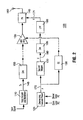
- FIG. 1 illustrates a simplified block diagram of a transmitter apparatus 100 in accordance with the present invention.
- the transmitter 100 comprises a data encoder and modulator 110.
- the data encoder and modulator 110 converts a digital signal to be transmitted to the modulation technique appropriate to the air interface standard in which the mobile is operating.
- the data encoder and modulator 110 uses CDMA modulation for use in an IS-2000 system.
- Other modulation schemes may include UMTS, 802.11, GSM, EDGE, TDMA, or others that are well known to those skilled in the art.
- the data encoder and modulator 110 generates a Tx signal 145 and a data format/data rate indicator that uniquely indicates a supported combination of data rate, coding and modulation method of the wireless mobile device, referred to herein as a data indicator "r" 150.
- the Tx signal 145 comprises data frames to be transmitted at variable data formats or data rates.
- the data indicator "r" 150 indicates the variable data rate and format at which the signal is being transmitted.
- the digital Tx signal 145 is converted to an analog signal by a digital-to-analog converter 155 prior to performing analog processing.
- Analog processing can include mixing to an intermediate frequency and filtering as well as any other necessary analog processes. In some embodiments, zero IF is used and mixing to an intermediate frequency is not required. Analog processing is well known in the art and is not discussed further.
- the amplitude of the analog processed signal is adjusted by an automatic gain control (AGC) amplifier 135. Control of the AGC amplifier 135 is discussed subsequently.
- the signal can then be converted from an intermediate frequency signal (or zero intermediate frequency signal) to an RF frequency for transmission. Alternatively the frequency conversion to an RF frequency is done before the AGC amplifier 135. Either way, the RF signal is input to an RF power amplifier 140 before being transmitted over the air interface by the antenna 160. Control of the power amplifier 140 bias is also discussed subsequently.
- the data indicator "r" 150 is mapped by the first mapper 115 to generate signal PAPR(r). This is the ratio of the peak signal power over the average signal power of signal 145 that corresponds to the data indicator "r" 150. This peak to average power ratio signal is designated as PAPR(r) 165. In one embodiment, PAPR(r) is in dB or proportional to dB.
- a desired average transmit power block 125 generates a desired average power indicator "p" 170.
- This block 125 uses an open loop power control method, a closed loop power control correction signal from the base station (preferably transmitted every 1.25 ms), and/or other base station parameters for the offset of power.
- the mobile device preferably uses the received total and pilot signal strengths and internal algorithms to estimate and adjust its own transmit power.
- the open loop powers can further be adjusted, on a continuous basis, by the closed loop power control commands that the mobile device receives from the base station.
- the desired average transmit power indicator "p" 170 varies with time.
- "p" has units of dBm and is updated at the same rate as the closed loop power control (e.g., 1.25 ms).
- PAPR(r) 165 and "p" 170 are summed by a summer 175 that generates a peak power value in dBm (or proportional to it) representing the peak transmit power of the Tx signal expected at antenna 160, which is the RF counterpart of baseband Tx signal 145 .
- This peak transmit power is mapped by the second mapper 120 to an effectively continuous "X" signal 180, whose value is effectively continuous in a range that is designed for.
- the generation of X 180 is as follows: for a given peak Tx power value, p+PAPR(r), determine the corresponding optimal X signal 180 that gives the best transmitter power efficiency while still meeting the out of band spurious emissions and rho (waveform quality) requirements.
- An array of such values for the X signal 180 is stored in the second mapper 120. In one embodiment, this relationship is non-linear. Interpolation may be used in the mapping to get fine resolution and save storage memory. The array of such values for a transmitter is determined by experimentation during calibration and testing of the transmitter.
- the "X" signal 180 is converted, to an analog signal by a D/A converter 185 and smoothed by a low pass filter LPF 190.
- the output of the LPF 190 is used to adjust a setting of the power amplifier 140.
- the setting in this embodiment is a bias voltage.
- the bias voltage "Y" is supplied to the power amplifier 140 control input port and is lowered or raised accordingly for optimal power efficiency in generating the power of the transmitted signal Tx 145 and its radio frequency counterpart 160.
- the indicator "p" 170 is also input to a gain control block 130 to generate a control signal that controls the Tx signal's gain with the AGC amplifier 135.
- the AGC control is well known in the art and is not discussed further.
- the delay of the Tx signal 145 to the output of antenna 160 is designed to be the same as the delay from "p" 170 or "r” 150 to the effects of "Y" 171 at antenna 160. These identical signal delays are referred to in the art as being delay aligned.
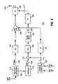
- FIG. 3 illustrates an alternate embodiment of the transmitter apparatus 100 of the present invention.
- the first mapper 115 and the summer 175 of the embodiment of FIG. 2 are eliminated.
- the second mapper 120 uses the average transmit power indicator "p" 170 as its input.
- the "X" signal 180 is determined as follows: for a given average transmit power indicator "p" 170, the corresponding optimal "X" signal 180 is generated that provides the best transmitter power efficiency while satisfying out of band spurious emissions and rho requirements.
- these signals that are stored in the second mapper's 120 array are determined by experimentation.
- the remainder of the embodiment of FIG. 3 is the same as the embodiment of FIG. 2 and is not discussed further.
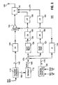
- FIG. 4 illustrates yet another embodiment of the transmitter apparatus 100 of the present invention.
- This embodiment uses multiple "X" signals that are provided to adjust multiple parts of the transmitter 100 or multiple parameters of the same part of the transmitter 100, instead of just one "X” signal 180 to adjust only one parameter of the power amplifier 140.
- the multiple "X” signals may be implemented by an array of second mappers 120 and 121, D/A converters 185 and 186, and low pass filters 190 and 191.
- Each individual element of "X” is determined as described in the above embodiment: to provide the best transmitter power efficiency while still satisfying out of band spurious emissions and rho requirements.
- the corresponding mapper may be implemented as a threshold comparator.
- the multiple "X" signals may also include additional input variables such as the transmitter temperature and battery voltage.
- the second mapper 120 then becomes multidimensional.
- Various simplified implementations (or approximations) of multidimensional mapping tables may also be used.
- FIG. 4 shows only 2 second mapper functions 120 and 121.
- the present invention is not limited to any one quantity of second mappers.
- the present invention is not meant to be limited to X being an input to the power amplifier 140, but instead can be used within other parts of transmitter 100.
- FIG. 5 illustrates yet another embodiment of the transmitter apparatus 100 of the present invention.
- the second mapper 120 may also be implemented by analog means and placed after the D/A converter 185. The functionality of the blocks remains the same as does the remainder of the transmitter, only the implementation of the second mapper 120 has been changed.
- signals X may control various devices within the transmitter, including a power amplifier, a stage or stages of a power amplifier, a drive amplifier, an AGC amplifier, a power supply to a power amplifier and/or other devices in a transmitter, a mixer, a matching network, a filtering means, a power combining or coupling means, a charging means, a voltage or current generation or regulation means, or other means, or,a combination of these.
- inputs such as the multiple X signals, to control certain transmitter circuit parameters may include (but are not limited to): (a) bias to each or some of the amplifying devices inside a power amplifier so that only the minimum bias is provided to obtain the required out of band spurious emissions and rho for each given transmitted power and/or PAPR values in the supported range; (b) power supply voltage(s) to all or selected stages of the power amplifier 140 and/or other circuits in the transmitter 100; such power supply voltages are supplied to the circuits so that only the minimum voltage is provided to obtain the required out of band spurious emissions and rho for each given transmitted power and/or PAPR values in the supported range; (c) to switch in or out, or turn on or off selected stages according to the transmitted power and/or PAPR values; and (d) gains of all or selected stages of the amplifying chains in the transmitter; (e) conducting angle of all or selected stages of the amplifying chains in the transmitter, (f) class of amplifying (e.g., Class A,
- the transmitter apparatus and power optimization method of the present invention provides improved power efficiency of transmitters having varying transmit power and high/variable PAPR. This provides a mobile, battery-powered device with increased battery life performance.
Landscapes
- Engineering & Computer Science (AREA)
- Computer Networks & Wireless Communication (AREA)
- Signal Processing (AREA)
- Transmitters (AREA)
- Amplifiers (AREA)
- Optical Communication System (AREA)
- Semiconductor Lasers (AREA)
Claims (13)
- Eine Sendevorrichtung (100) in einem drahtlosen mobilen Gerät, bestehend aus:einem Codierer und Modulator (110), der aus einem Eingangssignal ein codiertes und moduliertes Sendesignal sowie ein Datenindikatorsignal entsprechend der Art des codierten und modulierten Sendesignals erzeugt;einem Digital-Analog-Wandler (155), der an den Codierer und Modulator gekoppelt ist und ein Analogdarstellungssignal des codierten und modulierten Sendesignals erzeugt;einer ersten Zuweisungsfunktion (115), die an den Codierer und Modulator gekoppelt ist und als Reaktion auf das Datenindikatorsignal ein Signal für das Verhältnis zwischen Spitzen- und Durchschnittsleistung erzeugt;einem Summierer (175), der ein Signal für die Spitzensendeleistung als Summe aus dem Signal für das Verhältnis zwischen Spitzen- und Durchschnittsleistung und einem Signal für die gewünschte durchschnittliche Sendeleistung erzeugt;einer zweiten Zuweisungsfunktion (120), die als Reaktion auf das Signal für die Spitzensendeleistung ein praktisch wertkontinuierliches Signal zur Steuerung des Leistungsverstärkers erzeugt, wobei diese zweite Zuweisungsfunktion eine Tabelle mit einer Reihe von Signalwerten zur Steuerung des Leistungsverstärkers beinhaltet, die jeweils einem Spitzenwert der Sendeleistung entsprechen;einem Regelverstärker (135), der an den Digital-Analog-Wandler gekoppelt ist und als Reaktion auf das Signal für die gewünschte durchschnittliche Sendeleistung ein verstärktes Analogdarstellungssignal erzeugt; sowieeinem Leistungsverstärker (140) mit einem Eingangskanal, der an das verstärkte Analogdarstellungssignal gekoppelt ist, und einem Steuerungskanal, der an das Signal zur Steuerung des Leistungsverstärkers gekoppelt ist, wobei mindestens ein Parameter des Leistungsverstärkers als Reaktion auf das Signal zur Steuerung des Leistungsverstärkers so angepasst wird, dass das verstärkte Analogdarstellungssignal mit einem gewünschten Leistungswert mit optimiertem Wirkungsgrad übertragen wird und zugleich die Anforderungen im Hinblick auf Außerband-Nebenwellen und die Beschaffenheit der Wellenform weiterhin erfüllt werden.
- Die Vorrichtung (100) gemäß Anspruch 1, bei der die erste Zuweisungsfunktion (115) eine Tabelle mit einer Reihe von Werten für das Verhältnis zwischen Spitzen- und durchschnittlicher Sendeleistung beinhaltet, denen jeweils ein entsprechender Datenindikator zugeordnet ist.
- Die Vorrichtung (100) gemäß Anspruch 1 oder Anspruch 2, die darüber hinaus einen Digital-Analog-Wandler (185) beinhaltet, der so zwischen die zweite Zuweisungsfunktion 120) und den Leistungsverstärker (140) gekoppelt ist, dass das Signal zur Steuerung des Leistungsverstärkers in eine Analogdarstellung des Signals zur Steuerung des Leistungsverstärkers umgewandelt wird.
- Die Vorrichtung (100) gemäß jedem der Ansprüche 1 bis 3, bei der das Signal zur Steuerung des Leistungsverstärkers ein Analogsignal ist, das vor dem Leistungsverstärker (140) einen Tiefpassfilter durchläuft.
- Die Vorrichtung (100) gemäß jedem der Ansprüche 1 bis 4, bei der das Signal für die Spitzensendeleistung vor der Eingabe an die zweite Zuweisungsfunktion (120) in ein Analogsignal umgewandelt wird.
- Die Vorrichtung (100) gemäß jedem der Ansprüche 1 bis 5, die darüber hinaus einen Generator zur Indikation der gewünschten Leistung beinhaltet, der das Signal für die gewünschte durchschnittliche Sendeleistung als Reaktion auf ein Leistungssteuerungssignal mit offenem Regelkreis und ein Leistungssteuerungssignal mit geschlossenem Regelkreis erzeugt.
- Ein Verfahren zur Optimierung des Wirkungsgrads einer Sendevorrichtung (100), bestehend aus:der Erzeugung eines codierten und modulierten Signals aus einem digitalen Eingangssignal wie auch der Erzeugung eines Datenindikatorsignals entsprechend dem codierten und modulierten Signal;der Umwandlung des codierten und modulierten Signals in ein analoges Sendesignal;dem Auswählen (als Reaktion auf das Datenindikatorsignal) eines Signalwerts für das Verhältnis zwischen Spitzen- und durchschnittlicher Ausgangsleistung aus einer Reihe von Signalwerten für das Verhältnis zwischen Spitzen- und Durchschnittsleistung, denen jeweils eine entsprechende Datenrate oder ein entsprechendes Datenformat zugeordnet ist;dem Erzeugen eines Signalwerts für die gewünschte Sendeleistung;dem Summieren des Signalwerts für die gewünschte Sendeleistung und des Signalwerts für das Verhältnis zwischen Spitzen- und Durchschnittsleistung zur Erzeugung eines Signalwerts für die Spitzensendeleistung; sowiedem fortlaufenden Zuweisen des Werts des Signals für die Spitzensendeleistung zu einem Wert mindestens eines Steuerungssignals für mindestens ein Gerät innerhalb der besagten Sendevorrichtung zur Steuerung mindestens eines Parameters innerhalb der besagten Sendevorrichtung mit dem Ziel, den Wirkungsgrad der Sendevorrichtung zu optimieren, wobei die jeweilige Sendeleistung zu einem optimierten Wirkungsgrad des Senders führt und zugleich die Anforderungen im Hinblick auf Außerband-Nebenwellen und die Beschaffenheit der Wellenform weiterhin erfüllt werden.
- Das Verfahren gemäß Anspruch 7, bei dem das besagte mindestens eine Gerät innerhalb der besagten Sendevorrichtung ein Leistungsverstärker (140) ist.
- Das Verfahren gemäß Anspruch 7 oder Anspruch 8, bei dem das besagte Steuerungssignal ein Signal zur Steuerung eines Leistungsverstärkers ist.
- Das Verfahren gemäß jedem der Ansprüche 7 bis 9, bei dem die gewünschte Sendeleistung als Reaktion auf ein Leistungssteuerungssignal mit offenem Regelkreis und ein Leistungssteuerungssignal mit geschlossenem Regelkreis erzeugt wird.
- Das Verfahren gemäß jedem der Ansprüche 7 bis 10, bei dem das Steuerungssignal ein Digitalsignal ist und das darüber hinaus die Umwandlung des Steuerungssignals in ein Analogsignal vor der Anpassung mindestens eines Parameters von besagtem mindestens einem Gerät innerhalb der besagten Sendevorrichtung beinhaltet.
- Das Verfahren gemäß jedem der Ansprüche 7 bis 11, das darüber hinaus die Tiefpassfilterung des Steuerungssignals beinhaltet.
- Ein drahtloses mobiles Gerät, das die Sendevorrichtung (100) gemäß jedem der Ansprüche 1 bis 6 beinhaltet.
Applications Claiming Priority (3)
| Application Number | Priority Date | Filing Date | Title |
|---|---|---|---|
| US43029302P | 2002-12-02 | 2002-12-02 | |
| US430293P | 2002-12-02 | ||
| PCT/CA2003/001886 WO2004051843A2 (en) | 2002-12-02 | 2003-12-02 | Method and apparatus for optimizing transmitter power efficiency |
Publications (2)
| Publication Number | Publication Date |
|---|---|
| EP1568151A2 EP1568151A2 (de) | 2005-08-31 |
| EP1568151B1 true EP1568151B1 (de) | 2007-08-29 |
Family
ID=32469441
Family Applications (1)
| Application Number | Title | Priority Date | Filing Date |
|---|---|---|---|
| EP03779613A Expired - Lifetime EP1568151B1 (de) | 2002-12-02 | 2003-12-02 | Verfahren und vorrichtung zum optimieren des wirkungsgrads eines senders |
Country Status (7)
| Country | Link |
|---|---|
| US (4) | US7471738B2 (de) |
| EP (1) | EP1568151B1 (de) |
| AT (1) | ATE371994T1 (de) |
| AU (1) | AU2003287816A1 (de) |
| CA (1) | CA2506512C (de) |
| DE (2) | DE03779613T1 (de) |
| WO (1) | WO2004051843A2 (de) |
Cited By (6)
| Publication number | Priority date | Publication date | Assignee | Title |
|---|---|---|---|---|
| US8160517B2 (en) | 2006-06-14 | 2012-04-17 | Research In Motion Limited | Control of switcher regulated power amplifier modules |
| US8290085B2 (en) | 2004-02-20 | 2012-10-16 | Research In Motion Limited | Method and apparatus for improving power amplifier efficiency in wireless communication systems having high peak to average power ratios |
| US8295397B2 (en) | 2006-06-14 | 2012-10-23 | Research In Motion Limited | Input drive control for switcher regulated power amplifier modules |
| US8620238B2 (en) | 2010-07-23 | 2013-12-31 | Blackberry Limited | Method of power amplifier switching power control using post power amplifier power detection |
| US8761305B2 (en) | 2006-06-14 | 2014-06-24 | Blackberry Limited | Input drive control for switcher regulated power amplifier modules |
| US8873675B2 (en) | 2002-12-02 | 2014-10-28 | Blackberry Limited | Method and apparatus for optimizing transmitter power efficiency |
Families Citing this family (24)
| Publication number | Priority date | Publication date | Assignee | Title |
|---|---|---|---|---|
| FI115935B (fi) * | 2003-02-25 | 2005-08-15 | Nokia Corp | Menetelmä ja laite tehovahvistimen ominaisuuksien säätämiseksi |
| JP2006526916A (ja) * | 2003-05-09 | 2006-11-24 | コーニンクレッカ フィリップス エレクトロニクス エヌ ヴィ | 移動体通信装置の送信電力を設定するための方法および装置 |
| KR100703265B1 (ko) * | 2004-05-12 | 2007-04-03 | 삼성전자주식회사 | 멀티캐리어 변조 방식의 통신 시스템에서 피크-대-평균전력비를 감소시키는 송신기 및 수신기와 적응적피크-대-평균 전력비 제어 방법 |
| JP4340889B2 (ja) * | 2004-07-15 | 2009-10-07 | 横河電機株式会社 | 検査装置 |
| US7428426B2 (en) * | 2004-08-06 | 2008-09-23 | Qualcomm, Inc. | Method and apparatus for controlling transmit power in a wireless communications device |
| JP4175545B2 (ja) * | 2004-09-03 | 2008-11-05 | ソニー・エリクソン・モバイルコミュニケーションズ株式会社 | 無線通信端末 |
| GB0420847D0 (en) * | 2004-09-20 | 2004-10-20 | Koninkl Philips Electronics Nv | A radio communication system, a radio station, and a method of transmitting data |
| GB2421373B (en) * | 2004-12-17 | 2009-01-28 | Motorola Inc | A transmitter a transceiver and method of controlling a transmit power therefor |
| JP5255986B2 (ja) * | 2008-10-20 | 2013-08-07 | 株式会社日立ハイテクノロジーズ | パターンドメディアの検査方法及び検査装置 |
| TWI404357B (zh) * | 2008-12-10 | 2013-08-01 | Ind Tech Res Inst | 發射功率控制方法與系統 |
| US8948713B2 (en) * | 2009-06-16 | 2015-02-03 | Broadcom Corporation | Antenna impedance/power amplifier source impedance measurement circuitry and device operation based thereon |
| WO2011112909A2 (en) | 2010-03-12 | 2011-09-15 | Sunrise Micro Devices, Inc. | Power efficient communications |
| WO2013112609A1 (en) * | 2012-01-23 | 2013-08-01 | Utah State University | Switch wear leveling |
| WO2013123651A1 (en) * | 2012-02-22 | 2013-08-29 | Telefonaktiebolaget L M Ericsson(Publ) | Device and method for controlling an input signal of a power amplifier |
| KR102027628B1 (ko) | 2012-12-18 | 2019-10-01 | 트럼프 헛팅거 게엠베하 + 코 카게 | 고주파수 전력을 생산하기 위한 방법 및 부하에 전력을 공급하기 위한 전력 컨버터를 갖는 전력 공급 시스템 |
| DE102012223662B4 (de) * | 2012-12-18 | 2017-12-14 | TRUMPF Hüttinger GmbH + Co. KG | Verfahren zur Erzeugung einer Hochfrequenzleistung und Leistungsversorgungssystem mit einem Leistungswandler zur Versorgung einer Last mit Leistung |
| US9847676B2 (en) * | 2013-09-27 | 2017-12-19 | Intel IP Corporation | Power saving technique for digital to time converters |
| CN106773644B (zh) * | 2016-11-18 | 2017-09-29 | 国网山东省电力公司电力科学研究院 | 一种基于供热抽汽量变化的agc控制系统及其方法 |
| CN107769739A (zh) * | 2017-10-16 | 2018-03-06 | 广州慧智微电子有限公司 | 射频功率放大电路 |
| KR102098913B1 (ko) * | 2018-08-30 | 2020-04-08 | 성균관대학교 산학협력단 | Papr 기반 통신 방법 및 이를 이용한 송신 장치와 수신 장치 |
| WO2022138001A1 (ja) * | 2020-12-21 | 2022-06-30 | 株式会社村田製作所 | 高周波回路、高周波モジュールおよび通信装置 |
| US11765011B2 (en) | 2021-07-06 | 2023-09-19 | Huawei Technologies Co., Ltd. | Method and apparatus for transmitting and receiving data |
| US12495370B2 (en) * | 2022-03-11 | 2025-12-09 | Apple Inc. | Method for multiple power class support |
| US11870512B2 (en) | 2022-04-27 | 2024-01-09 | Samsung Electronics Co., Ltd. | Distributed closed-loop power control with VGA gain update |
Family Cites Families (24)
| Publication number | Priority date | Publication date | Assignee | Title |
|---|---|---|---|---|
| US4849711A (en) * | 1987-09-04 | 1989-07-18 | Digital Equipment Corporation | Automatic gain control system |
| US6236365B1 (en) * | 1996-09-09 | 2001-05-22 | Tracbeam, Llc | Location of a mobile station using a plurality of commercial wireless infrastructures |
| US6205127B1 (en) * | 1998-04-21 | 2001-03-20 | Lucent Technologies, Inc. | Wireless telecommunications system that mitigates the effect of multipath fading |
| US6043707A (en) * | 1999-01-07 | 2000-03-28 | Motorola, Inc. | Method and apparatus for operating a radio-frequency power amplifier as a variable-class linear amplifier |
| US6166598A (en) * | 1999-07-22 | 2000-12-26 | Motorola, Inc. | Power amplifying circuit with supply adjust to control adjacent and alternate channel power |
| US6349216B1 (en) * | 1999-07-22 | 2002-02-19 | Motorola, Inc. | Load envelope following amplifier system |
| US6965676B1 (en) * | 1999-10-19 | 2005-11-15 | Texas Instruments Incorporated | Volume-responsive loudness compensation circuits, systems, and methods |
| EP1162766B1 (de) * | 1999-12-24 | 2008-02-27 | NTT DoCoMo, Inc. | Verfahren und gerät zur übertragung von burst signalen in einem mobilen kommunikationssystem, nachrichtenverteilungsverfahren, und nachrichtenverteilungssteuerer |
| EP1128626B1 (de) * | 2000-02-28 | 2005-08-24 | Lucent Technologies Inc. | Sender mit einer geschlossenen Rückkopplung zur Modulation |
| US6597925B1 (en) * | 2000-03-16 | 2003-07-22 | Agere Systems Inc. | Transmitter circuit with frequency self-optimization |
| US7110721B2 (en) * | 2000-04-25 | 2006-09-19 | Advantest Corporation | Apparatus, method and program for communication test, and recorded medium on which that program has been recorded |
| US6862457B1 (en) * | 2000-06-21 | 2005-03-01 | Qualcomm Incorporated | Method and apparatus for adaptive reverse link power control using mobility profiles |
| KR100358120B1 (ko) * | 2000-10-20 | 2002-10-25 | 한국전자통신연구원 | 동일대역 인접채널 방식의 디지털 오디오 방송 전송 시스템 |
| US6674999B2 (en) | 2001-03-16 | 2004-01-06 | Skyworks Solutions, Inc | Dynamically varying linearity system for an RF front-end of a communication device |
| US6535066B1 (en) * | 2001-06-21 | 2003-03-18 | Cisco Technology, Inc. | Dynamic RF amplifier bias control for digital wireless communications devices |
| SE0103683D0 (sv) | 2001-11-06 | 2001-11-06 | Ericsson Telefon Ab L M | Method and arrangement in a communication system |
| US7224742B2 (en) * | 2001-12-14 | 2007-05-29 | Samsung Electronics Co., Ltd. | Apparatus and method for reducing the peak-to-average power ratio of OFDM/OFDMA signals |
| US6985751B2 (en) * | 2002-03-07 | 2006-01-10 | Siemens Communications, Inc. | Combined open and closed loop power control with differential measurement |
| US6985704B2 (en) * | 2002-05-01 | 2006-01-10 | Dali Yang | System and method for digital memorized predistortion for wireless communication |
| US6891902B2 (en) * | 2002-07-02 | 2005-05-10 | Intel Corporation | System and method for adjusting a power level of a transmission signal |
| WO2004023668A1 (en) * | 2002-09-05 | 2004-03-18 | The Regents Of The University Of California | Scheduling methods for wireless networks |
| US20040100921A1 (en) * | 2002-11-27 | 2004-05-27 | Farooq Ullah Khan | Time-orthogonal CDMA wireless communication system |
| US6765440B2 (en) * | 2002-12-18 | 2004-07-20 | Andrew Corporation | Model-based feed-forward linearization of amplifiers |
| US6917244B2 (en) * | 2003-06-10 | 2005-07-12 | Nokia Corporation | Power control for a switching mode power amplifier |
-
2003
- 2003-12-01 US US10/724,951 patent/US7471738B2/en not_active Expired - Lifetime
- 2003-12-02 AT AT03779613T patent/ATE371994T1/de not_active IP Right Cessation
- 2003-12-02 AU AU2003287816A patent/AU2003287816A1/en not_active Abandoned
- 2003-12-02 DE DE03779613T patent/DE03779613T1/de active Pending
- 2003-12-02 WO PCT/CA2003/001886 patent/WO2004051843A2/en not_active Ceased
- 2003-12-02 EP EP03779613A patent/EP1568151B1/de not_active Expired - Lifetime
- 2003-12-02 DE DE60316022T patent/DE60316022T2/de not_active Expired - Lifetime
- 2003-12-02 CA CA2506512A patent/CA2506512C/en not_active Expired - Lifetime
-
2008
- 2008-11-24 US US12/276,650 patent/US7852968B2/en not_active Expired - Lifetime
-
2010
- 2010-11-09 US US12/942,757 patent/US8098761B2/en not_active Expired - Lifetime
-
2011
- 2011-12-14 US US13/325,895 patent/US8599963B2/en not_active Expired - Fee Related
Cited By (10)
| Publication number | Priority date | Publication date | Assignee | Title |
|---|---|---|---|---|
| US8873675B2 (en) | 2002-12-02 | 2014-10-28 | Blackberry Limited | Method and apparatus for optimizing transmitter power efficiency |
| US8290085B2 (en) | 2004-02-20 | 2012-10-16 | Research In Motion Limited | Method and apparatus for improving power amplifier efficiency in wireless communication systems having high peak to average power ratios |
| US8670503B2 (en) | 2004-02-20 | 2014-03-11 | Blackberry Limited | Method and apparatus for improving power amplifier efficiency in wireless communication systems having high peak to average power ratios |
| US8160517B2 (en) | 2006-06-14 | 2012-04-17 | Research In Motion Limited | Control of switcher regulated power amplifier modules |
| US8295792B2 (en) | 2006-06-14 | 2012-10-23 | Research In Motion Limited | Control of switcher regulated power amplifier modules |
| US8295397B2 (en) | 2006-06-14 | 2012-10-23 | Research In Motion Limited | Input drive control for switcher regulated power amplifier modules |
| US8606199B2 (en) | 2006-06-14 | 2013-12-10 | Blackberry Limited | Control of switcher regulated power amplifier modules |
| US8761305B2 (en) | 2006-06-14 | 2014-06-24 | Blackberry Limited | Input drive control for switcher regulated power amplifier modules |
| US8620238B2 (en) | 2010-07-23 | 2013-12-31 | Blackberry Limited | Method of power amplifier switching power control using post power amplifier power detection |
| US9276545B2 (en) | 2010-07-23 | 2016-03-01 | Blackberry Limited | Method of power amplifier switching power control using post power amplifier power detection |
Also Published As
| Publication number | Publication date |
|---|---|
| US8098761B2 (en) | 2012-01-17 |
| CA2506512A1 (en) | 2004-06-17 |
| US7852968B2 (en) | 2010-12-14 |
| CA2506512C (en) | 2010-05-11 |
| US20110053533A1 (en) | 2011-03-03 |
| US8599963B2 (en) | 2013-12-03 |
| DE60316022T2 (de) | 2008-06-05 |
| AU2003287816A1 (en) | 2004-06-23 |
| DE60316022D1 (de) | 2007-10-11 |
| US7471738B2 (en) | 2008-12-30 |
| WO2004051843A3 (en) | 2004-11-04 |
| US20090074107A1 (en) | 2009-03-19 |
| DE03779613T1 (de) | 2006-03-23 |
| US20120087441A1 (en) | 2012-04-12 |
| HK1080228A1 (en) | 2006-04-21 |
| ATE371994T1 (de) | 2007-09-15 |
| US20040208260A1 (en) | 2004-10-21 |
| EP1568151A2 (de) | 2005-08-31 |
| AU2003287816A8 (en) | 2004-06-23 |
| WO2004051843A2 (en) | 2004-06-17 |
Similar Documents
| Publication | Publication Date | Title |
|---|---|---|
| US8599963B2 (en) | Method and apparatus for optimizing transmitter power efficiency | |
| US8428181B2 (en) | Method and apparatus for optimizing transmitter power efficiency | |
| US8000409B2 (en) | Method and apparatus for improving power amplifier efficiency in wireless communication systems having high peak to average power ratios | |
| US5708681A (en) | Hybrid analog/digital method and apparatus for controlling the transmission power level of a radio transceiver | |
| US7539466B2 (en) | Amplifier with varying supply voltage and input attenuation based upon supply voltage | |
| CA2497038C (en) | Method and apparatus for improving power amplifier efficiency in wireless communication systems having high peak to average power ratios | |
| EP1597824B1 (de) | Verfahren und einrichtung zur einstellung von leistungsverstärkereigenschaften | |
| CN1164027C (zh) | 具有供电调整以控制相邻和相间信道功率的功率放大电路 | |
| JPH06507774A (ja) | 高効率二重モード増幅装置 | |
| JP4511353B2 (ja) | 携帯端末の電力増幅器の動作基点を最適化する方法及び携帯通信端末 | |
| CN100456641C (zh) | 用于最优化发射机功率效率的方法和装置 | |
| HK1080228B (en) | Method and apparatus for optimizing transmitter power efficiency | |
| HK1161444B (en) | Method and apparatus for optimizing transmitter power efficiency | |
| HK1161444A (en) | Method and apparatus for optimizing transmitter power efficiency |
Legal Events
| Date | Code | Title | Description |
|---|---|---|---|
| PUAI | Public reference made under article 153(3) epc to a published international application that has entered the european phase |
Free format text: ORIGINAL CODE: 0009012 |
|
| 17P | Request for examination filed |
Effective date: 20050530 |
|
| AK | Designated contracting states |
Kind code of ref document: A2 Designated state(s): AT BE BG CH CY CZ DE DK EE ES FI FR GB GR HU IE IT LI LU MC NL PT RO SE SI SK TR |
|
| AX | Request for extension of the european patent |
Extension state: AL LT LV MK |
|
| EL | Fr: translation of claims filed | ||
| GRAP | Despatch of communication of intention to grant a patent |
Free format text: ORIGINAL CODE: EPIDOSNIGR1 |
|
| DET | De: translation of patent claims | ||
| REG | Reference to a national code |
Ref country code: HK Ref legal event code: DE Ref document number: 1080228 Country of ref document: HK |
|
| GRAS | Grant fee paid |
Free format text: ORIGINAL CODE: EPIDOSNIGR3 |
|
| GRAA | (expected) grant |
Free format text: ORIGINAL CODE: 0009210 |
|
| AK | Designated contracting states |
Kind code of ref document: B1 Designated state(s): AT BE BG CH CY CZ DE DK EE ES FI FR GB GR HU IE IT LI LU MC NL PT RO SE SI SK TR |
|
| AX | Request for extension of the european patent |
Extension state: AL LT LV MK |
|
| REG | Reference to a national code |
Ref country code: GB Ref legal event code: FG4D |
|
| REG | Reference to a national code |
Ref country code: CH Ref legal event code: EP |
|
| REG | Reference to a national code |
Ref country code: IE Ref legal event code: FG4D |
|
| REF | Corresponds to: |
Ref document number: 60316022 Country of ref document: DE Date of ref document: 20071011 Kind code of ref document: P |
|
| REG | Reference to a national code |
Ref country code: HK Ref legal event code: GR Ref document number: 1080228 Country of ref document: HK |
|
| ET | Fr: translation filed | ||
| PG25 | Lapsed in a contracting state [announced via postgrant information from national office to epo] |
Ref country code: FI Free format text: LAPSE BECAUSE OF FAILURE TO SUBMIT A TRANSLATION OF THE DESCRIPTION OR TO PAY THE FEE WITHIN THE PRESCRIBED TIME-LIMIT Effective date: 20070829 Ref country code: NL Free format text: LAPSE BECAUSE OF FAILURE TO SUBMIT A TRANSLATION OF THE DESCRIPTION OR TO PAY THE FEE WITHIN THE PRESCRIBED TIME-LIMIT Effective date: 20070829 Ref country code: ES Free format text: LAPSE BECAUSE OF FAILURE TO SUBMIT A TRANSLATION OF THE DESCRIPTION OR TO PAY THE FEE WITHIN THE PRESCRIBED TIME-LIMIT Effective date: 20071210 |
|
| NLV1 | Nl: lapsed or annulled due to failure to fulfill the requirements of art. 29p and 29m of the patents act | ||
| LTIE | Lt: invalidation of european patent or patent extension |
Effective date: 20070829 |
|
| PG25 | Lapsed in a contracting state [announced via postgrant information from national office to epo] |
Ref country code: AT Free format text: LAPSE BECAUSE OF FAILURE TO SUBMIT A TRANSLATION OF THE DESCRIPTION OR TO PAY THE FEE WITHIN THE PRESCRIBED TIME-LIMIT Effective date: 20070829 Ref country code: CH Free format text: LAPSE BECAUSE OF FAILURE TO SUBMIT A TRANSLATION OF THE DESCRIPTION OR TO PAY THE FEE WITHIN THE PRESCRIBED TIME-LIMIT Effective date: 20070829 Ref country code: LI Free format text: LAPSE BECAUSE OF FAILURE TO SUBMIT A TRANSLATION OF THE DESCRIPTION OR TO PAY THE FEE WITHIN THE PRESCRIBED TIME-LIMIT Effective date: 20070829 |
|
| REG | Reference to a national code |
Ref country code: CH Ref legal event code: PL |
|
| PG25 | Lapsed in a contracting state [announced via postgrant information from national office to epo] |
Ref country code: BE Free format text: LAPSE BECAUSE OF FAILURE TO SUBMIT A TRANSLATION OF THE DESCRIPTION OR TO PAY THE FEE WITHIN THE PRESCRIBED TIME-LIMIT Effective date: 20070829 |
|
| PG25 | Lapsed in a contracting state [announced via postgrant information from national office to epo] |
Ref country code: DK Free format text: LAPSE BECAUSE OF FAILURE TO SUBMIT A TRANSLATION OF THE DESCRIPTION OR TO PAY THE FEE WITHIN THE PRESCRIBED TIME-LIMIT Effective date: 20070829 Ref country code: GR Free format text: LAPSE BECAUSE OF FAILURE TO SUBMIT A TRANSLATION OF THE DESCRIPTION OR TO PAY THE FEE WITHIN THE PRESCRIBED TIME-LIMIT Effective date: 20071130 |
|
| PG25 | Lapsed in a contracting state [announced via postgrant information from national office to epo] |
Ref country code: PT Free format text: LAPSE BECAUSE OF FAILURE TO SUBMIT A TRANSLATION OF THE DESCRIPTION OR TO PAY THE FEE WITHIN THE PRESCRIBED TIME-LIMIT Effective date: 20080129 Ref country code: SK Free format text: LAPSE BECAUSE OF FAILURE TO SUBMIT A TRANSLATION OF THE DESCRIPTION OR TO PAY THE FEE WITHIN THE PRESCRIBED TIME-LIMIT Effective date: 20070829 Ref country code: CZ Free format text: LAPSE BECAUSE OF FAILURE TO SUBMIT A TRANSLATION OF THE DESCRIPTION OR TO PAY THE FEE WITHIN THE PRESCRIBED TIME-LIMIT Effective date: 20070829 |
|
| PG25 | Lapsed in a contracting state [announced via postgrant information from national office to epo] |
Ref country code: RO Free format text: LAPSE BECAUSE OF FAILURE TO SUBMIT A TRANSLATION OF THE DESCRIPTION OR TO PAY THE FEE WITHIN THE PRESCRIBED TIME-LIMIT Effective date: 20070829 Ref country code: SE Free format text: LAPSE BECAUSE OF FAILURE TO SUBMIT A TRANSLATION OF THE DESCRIPTION OR TO PAY THE FEE WITHIN THE PRESCRIBED TIME-LIMIT Effective date: 20071129 |
|
| PLBE | No opposition filed within time limit |
Free format text: ORIGINAL CODE: 0009261 |
|
| STAA | Information on the status of an ep patent application or granted ep patent |
Free format text: STATUS: NO OPPOSITION FILED WITHIN TIME LIMIT |
|
| PG25 | Lapsed in a contracting state [announced via postgrant information from national office to epo] |
Ref country code: MC Free format text: LAPSE BECAUSE OF NON-PAYMENT OF DUE FEES Effective date: 20071231 |
|
| 26N | No opposition filed |
Effective date: 20080530 |
|
| PG25 | Lapsed in a contracting state [announced via postgrant information from national office to epo] |
Ref country code: IE Free format text: LAPSE BECAUSE OF NON-PAYMENT OF DUE FEES Effective date: 20071203 |
|
| PG25 | Lapsed in a contracting state [announced via postgrant information from national office to epo] |
Ref country code: EE Free format text: LAPSE BECAUSE OF FAILURE TO SUBMIT A TRANSLATION OF THE DESCRIPTION OR TO PAY THE FEE WITHIN THE PRESCRIBED TIME-LIMIT Effective date: 20070829 |
|
| PG25 | Lapsed in a contracting state [announced via postgrant information from national office to epo] |
Ref country code: SI Free format text: LAPSE BECAUSE OF FAILURE TO SUBMIT A TRANSLATION OF THE DESCRIPTION OR TO PAY THE FEE WITHIN THE PRESCRIBED TIME-LIMIT Effective date: 20070829 |
|
| PG25 | Lapsed in a contracting state [announced via postgrant information from national office to epo] |
Ref country code: CY Free format text: LAPSE BECAUSE OF FAILURE TO SUBMIT A TRANSLATION OF THE DESCRIPTION OR TO PAY THE FEE WITHIN THE PRESCRIBED TIME-LIMIT Effective date: 20070829 |
|
| PG25 | Lapsed in a contracting state [announced via postgrant information from national office to epo] |
Ref country code: LU Free format text: LAPSE BECAUSE OF NON-PAYMENT OF DUE FEES Effective date: 20071202 Ref country code: BG Free format text: LAPSE BECAUSE OF FAILURE TO SUBMIT A TRANSLATION OF THE DESCRIPTION OR TO PAY THE FEE WITHIN THE PRESCRIBED TIME-LIMIT Effective date: 20071129 |
|
| PG25 | Lapsed in a contracting state [announced via postgrant information from national office to epo] |
Ref country code: TR Free format text: LAPSE BECAUSE OF FAILURE TO SUBMIT A TRANSLATION OF THE DESCRIPTION OR TO PAY THE FEE WITHIN THE PRESCRIBED TIME-LIMIT Effective date: 20070829 Ref country code: HU Free format text: LAPSE BECAUSE OF FAILURE TO SUBMIT A TRANSLATION OF THE DESCRIPTION OR TO PAY THE FEE WITHIN THE PRESCRIBED TIME-LIMIT Effective date: 20080301 |
|
| PG25 | Lapsed in a contracting state [announced via postgrant information from national office to epo] |
Ref country code: IT Free format text: LAPSE BECAUSE OF NON-PAYMENT OF DUE FEES Effective date: 20071231 |
|
| REG | Reference to a national code |
Ref country code: DE Ref legal event code: R082 Ref document number: 60316022 Country of ref document: DE Representative=s name: MERH-IP MATIAS ERNY REICHL HOFFMANN, DE |
|
| REG | Reference to a national code |
Ref country code: DE Ref legal event code: R082 Ref document number: 60316022 Country of ref document: DE Representative=s name: MERH-IP MATIAS ERNY REICHL HOFFMANN, DE Effective date: 20140925 Ref country code: DE Ref legal event code: R081 Ref document number: 60316022 Country of ref document: DE Owner name: BLACKBERRY LIMITED, WATERLOO, CA Free format text: FORMER OWNER: RESEARCH IN MOTION LTD., WATERLOO, ONTARIO, CA Effective date: 20140925 Ref country code: DE Ref legal event code: R082 Ref document number: 60316022 Country of ref document: DE Representative=s name: MERH-IP MATIAS ERNY REICHL HOFFMANN PATENTANWA, DE Effective date: 20140925 |
|
| REG | Reference to a national code |
Ref country code: FR Ref legal event code: PLFP Year of fee payment: 13 |
|
| REG | Reference to a national code |
Ref country code: FR Ref legal event code: PLFP Year of fee payment: 14 |
|
| REG | Reference to a national code |
Ref country code: FR Ref legal event code: PLFP Year of fee payment: 15 |
|
| PGFP | Annual fee paid to national office [announced via postgrant information from national office to epo] |
Ref country code: GB Payment date: 20221227 Year of fee payment: 20 Ref country code: FR Payment date: 20221227 Year of fee payment: 20 |
|
| PGFP | Annual fee paid to national office [announced via postgrant information from national office to epo] |
Ref country code: DE Payment date: 20221228 Year of fee payment: 20 |
|
| REG | Reference to a national code |
Ref country code: DE Ref legal event code: R071 Ref document number: 60316022 Country of ref document: DE |
|
| REG | Reference to a national code |
Ref country code: GB Ref legal event code: PE20 Expiry date: 20231201 |
|
| PG25 | Lapsed in a contracting state [announced via postgrant information from national office to epo] |
Ref country code: GB Free format text: LAPSE BECAUSE OF EXPIRATION OF PROTECTION Effective date: 20231201 |
|
| PG25 | Lapsed in a contracting state [announced via postgrant information from national office to epo] |
Ref country code: GB Free format text: LAPSE BECAUSE OF EXPIRATION OF PROTECTION Effective date: 20231201 |