EP1566845A1 - Photoelectric conversion element - Google Patents
Photoelectric conversion element Download PDFInfo
- Publication number
- EP1566845A1 EP1566845A1 EP03751417A EP03751417A EP1566845A1 EP 1566845 A1 EP1566845 A1 EP 1566845A1 EP 03751417 A EP03751417 A EP 03751417A EP 03751417 A EP03751417 A EP 03751417A EP 1566845 A1 EP1566845 A1 EP 1566845A1
- Authority
- EP
- European Patent Office
- Prior art keywords
- electron
- formula
- photoelectric converting
- derivative
- molecular structure
- Prior art date
- Legal status (The legal status is an assumption and is not a legal conclusion. Google has not performed a legal analysis and makes no representation as to the accuracy of the status listed.)
- Withdrawn
Links
Images

Classifications
-
- H—ELECTRICITY
- H10—SEMICONDUCTOR DEVICES; ELECTRIC SOLID-STATE DEVICES NOT OTHERWISE PROVIDED FOR
- H10K—ORGANIC ELECTRIC SOLID-STATE DEVICES
- H10K85/00—Organic materials used in the body or electrodes of devices covered by this subclass
- H10K85/20—Carbon compounds, e.g. carbon nanotubes or fullerenes
- H10K85/211—Fullerenes, e.g. C60
- H10K85/215—Fullerenes, e.g. C60 comprising substituents, e.g. PCBM
-
- B—PERFORMING OPERATIONS; TRANSPORTING
- B82—NANOTECHNOLOGY
- B82Y—SPECIFIC USES OR APPLICATIONS OF NANOSTRUCTURES; MEASUREMENT OR ANALYSIS OF NANOSTRUCTURES; MANUFACTURE OR TREATMENT OF NANOSTRUCTURES
- B82Y10/00—Nanotechnology for information processing, storage or transmission, e.g. quantum computing or single electron logic
-
- H—ELECTRICITY
- H01—ELECTRIC ELEMENTS
- H01G—CAPACITORS; CAPACITORS, RECTIFIERS, DETECTORS, SWITCHING DEVICES, LIGHT-SENSITIVE OR TEMPERATURE-SENSITIVE DEVICES OF THE ELECTROLYTIC TYPE
- H01G9/00—Electrolytic capacitors, rectifiers, detectors, switching devices, light-sensitive or temperature-sensitive devices; Processes of their manufacture
- H01G9/20—Light-sensitive devices
- H01G9/2004—Light-sensitive devices characterised by the electrolyte, e.g. comprising an organic electrolyte
-
- H—ELECTRICITY
- H10—SEMICONDUCTOR DEVICES; ELECTRIC SOLID-STATE DEVICES NOT OTHERWISE PROVIDED FOR
- H10K—ORGANIC ELECTRIC SOLID-STATE DEVICES
- H10K85/00—Organic materials used in the body or electrodes of devices covered by this subclass
- H10K85/10—Organic polymers or oligomers
- H10K85/111—Organic polymers or oligomers comprising aromatic, heteroaromatic, or aryl chains, e.g. polyaniline, polyphenylene or polyphenylene vinylene
- H10K85/114—Poly-phenylenevinylene; Derivatives thereof
-
- H—ELECTRICITY
- H10—SEMICONDUCTOR DEVICES; ELECTRIC SOLID-STATE DEVICES NOT OTHERWISE PROVIDED FOR
- H10K—ORGANIC ELECTRIC SOLID-STATE DEVICES
- H10K71/00—Manufacture or treatment specially adapted for the organic devices covered by this subclass
- H10K71/30—Doping active layers, e.g. electron transporting layers
-
- H—ELECTRICITY
- H10—SEMICONDUCTOR DEVICES; ELECTRIC SOLID-STATE DEVICES NOT OTHERWISE PROVIDED FOR
- H10K—ORGANIC ELECTRIC SOLID-STATE DEVICES
- H10K85/00—Organic materials used in the body or electrodes of devices covered by this subclass
- H10K85/10—Organic polymers or oligomers
- H10K85/111—Organic polymers or oligomers comprising aromatic, heteroaromatic, or aryl chains, e.g. polyaniline, polyphenylene or polyphenylene vinylene
- H10K85/113—Heteroaromatic compounds comprising sulfur or selene, e.g. polythiophene
- H10K85/1135—Polyethylene dioxythiophene [PEDOT]; Derivatives thereof
-
- H—ELECTRICITY
- H10—SEMICONDUCTOR DEVICES; ELECTRIC SOLID-STATE DEVICES NOT OTHERWISE PROVIDED FOR
- H10K—ORGANIC ELECTRIC SOLID-STATE DEVICES
- H10K85/00—Organic materials used in the body or electrodes of devices covered by this subclass
- H10K85/30—Coordination compounds
- H10K85/311—Phthalocyanine
-
- H—ELECTRICITY
- H10—SEMICONDUCTOR DEVICES; ELECTRIC SOLID-STATE DEVICES NOT OTHERWISE PROVIDED FOR
- H10K—ORGANIC ELECTRIC SOLID-STATE DEVICES
- H10K85/00—Organic materials used in the body or electrodes of devices covered by this subclass
- H10K85/60—Organic compounds having low molecular weight
- H10K85/611—Charge transfer complexes
-
- H—ELECTRICITY
- H10—SEMICONDUCTOR DEVICES; ELECTRIC SOLID-STATE DEVICES NOT OTHERWISE PROVIDED FOR
- H10K—ORGANIC ELECTRIC SOLID-STATE DEVICES
- H10K85/00—Organic materials used in the body or electrodes of devices covered by this subclass
- H10K85/60—Organic compounds having low molecular weight
- H10K85/615—Polycyclic condensed aromatic hydrocarbons, e.g. anthracene
- H10K85/621—Aromatic anhydride or imide compounds, e.g. perylene tetra-carboxylic dianhydride or perylene tetracarboxylic di-imide
-
- Y—GENERAL TAGGING OF NEW TECHNOLOGICAL DEVELOPMENTS; GENERAL TAGGING OF CROSS-SECTIONAL TECHNOLOGIES SPANNING OVER SEVERAL SECTIONS OF THE IPC; TECHNICAL SUBJECTS COVERED BY FORMER USPC CROSS-REFERENCE ART COLLECTIONS [XRACs] AND DIGESTS
- Y02—TECHNOLOGIES OR APPLICATIONS FOR MITIGATION OR ADAPTATION AGAINST CLIMATE CHANGE
- Y02E—REDUCTION OF GREENHOUSE GAS [GHG] EMISSIONS, RELATED TO ENERGY GENERATION, TRANSMISSION OR DISTRIBUTION
- Y02E10/00—Energy generation through renewable energy sources
- Y02E10/50—Photovoltaic [PV] energy
- Y02E10/549—Organic PV cells
-
- Y—GENERAL TAGGING OF NEW TECHNOLOGICAL DEVELOPMENTS; GENERAL TAGGING OF CROSS-SECTIONAL TECHNOLOGIES SPANNING OVER SEVERAL SECTIONS OF THE IPC; TECHNICAL SUBJECTS COVERED BY FORMER USPC CROSS-REFERENCE ART COLLECTIONS [XRACs] AND DIGESTS
- Y02—TECHNOLOGIES OR APPLICATIONS FOR MITIGATION OR ADAPTATION AGAINST CLIMATE CHANGE
- Y02P—CLIMATE CHANGE MITIGATION TECHNOLOGIES IN THE PRODUCTION OR PROCESSING OF GOODS
- Y02P70/00—Climate change mitigation technologies in the production process for final industrial or consumer products
- Y02P70/50—Manufacturing or production processes characterised by the final manufactured product
Definitions
- the present invention relates to photoelectric converting devices useful for photovoltaic generators or photovoltaic generating systems.
- Organic compounds are inexpensive and give less affect to the environment even though being disposed by incineration after use. With this background in view, development of a photoelectric converting device using organic photoelectric converting substances is one of the most important energy measures.
- the present invention was made in view of the above-described circumstances and thus relates to a photoelectric converting material enabling a production of a photoelectric converting layer excellent in a capability to suppress the phase separation and also to a photoelectric converting device using the photoelectric converting material.
- the present invention was achieved based on the finding that an photoelectric converting device with excellent properties that it is suppressed in the phase separation of the photoelectric converting layer and thus enhanced in the light utilizing efficiency can be produced by dispersing a specific compound in a polymer forming the photoelectric converting layer.
- the present invention relates to a photoelectric converting device which has a photoelectric converting layer comprising an organic compound (A) having both an electron donating molecular structure and an electron accepting molecular structure dispersed in a polymer.
- the present invention also relates to a photoelectric converting device which has a photoelectric converting layer comprising an organic compound (B) having an electron donating molecular structure and an organic compound (C) having an electron accepting molecular structure, dispersed in a polymer.
- a polymer constituting the photoelectric converting layer of the photoelectric converting device of the present invention No particular limitation is imposed on the polymer as long as it can disperse an organic compound (A) having both an electron donating molecular structure and an electron accepting molecular structure (hereinafter referred to as Compound (A))or both an organic compound (B) having an electron donating molecular structure (hereinafter referred to as Compound (B)) and an organic compound (C) having an electron accepting molecular structure (hereinafter referred to as Compound (C)).
- Compound (A) an organic compound having both an electron donating molecular structure and an electron accepting molecular structure
- Compound (B) organic compound having an electron donating molecular structure
- Compound (C) organic compound having an electron accepting molecular structure
- polymer examples include acrylic polymers such as polymethylmethacrylate and polyethylacrylate; polyethers such as polyethylene oxide and polypropylene oxide; polyesters such as polyethylene terephthalate; electrically conductive polymer compounds such as polyphenylene vinylene, polyacetylene, polythiophene, and polypyrrole. More preferred among these compounds are electrically conductive polymer compounds.
- Preferred electrically conductive polymer compounds are those having an electric conductivity of generally 10 -6 to 10 6 S/cm and more preferably 10 -4 to 10 5 S/cm, at a temperature of 20°C.
- the polymer may be any of those having a molecular weight of usually 1,000 to 5,000,000, preferably 10,000 to 1,000,000 and more preferably 50,000 to 500,000.
- the content of Compound (A) having both an electron donating molecular structure and an electron accepting molecular structure is usually from 5 to 300 parts by mass, preferably 10 to 100 parts by mass and more preferably 20 to 80 parts by mass, based on 100 parts by mass of the polymer.
- the content of Compound (B) having an electron donating molecular structure is usually from 5 to 300 parts by mass, preferably 10 to 100 parts by mass and more preferably 20 to 80 parts by mass, based on 100 parts by mass of the polymer while the content of Compound (C) having an electron accepting molecular structure is usually from 5 to 300 parts by mass, preferably 10 to 100 parts by mass and more preferably 20 to 80 parts by mass, based on 100 parts by mass of the polymer.
- the ratio of Compound (B) having an electron donating molecular structure to Compound (C) having an electron accepting molecular structure is usually from 10/90 to 90/10 and preferably 20/80 to 80/20.
- electrostatic molecular structure used herein denotes a structure exhibiting properties that the molecules are small in ionization potential and likely to become positive ions per se by supplying electrons to other molecules
- electron-accepting molecular structure denotes a structure exhibiting properties that the molecules are large in electron affinity and likely to become negative ions per se by accepting electrons from other molecules.
- molecular structure having electron-donating properties No particular limitation is imposed on the molecular structure having electron-donating properties as long as it has electron-donating properties in the molecular structure portion.
- the structure include amine, metallocene, polyarylene vinylene, polyanyline, polythiophene, polypyrrole and polyamine structures.
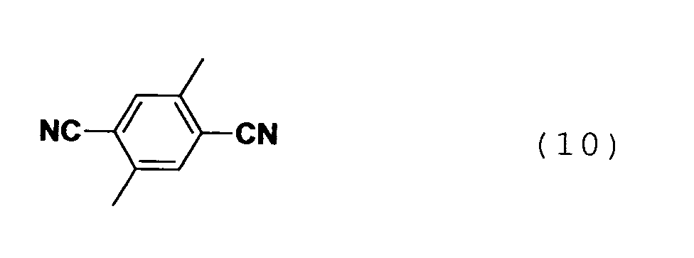
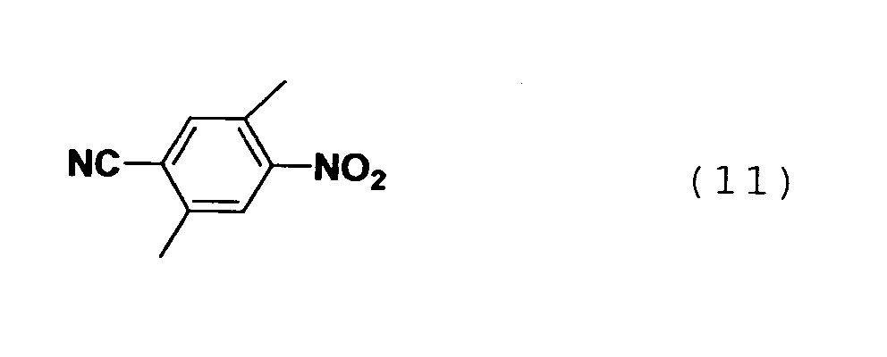
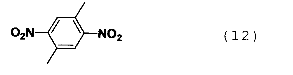
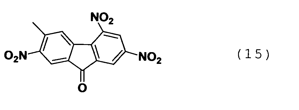
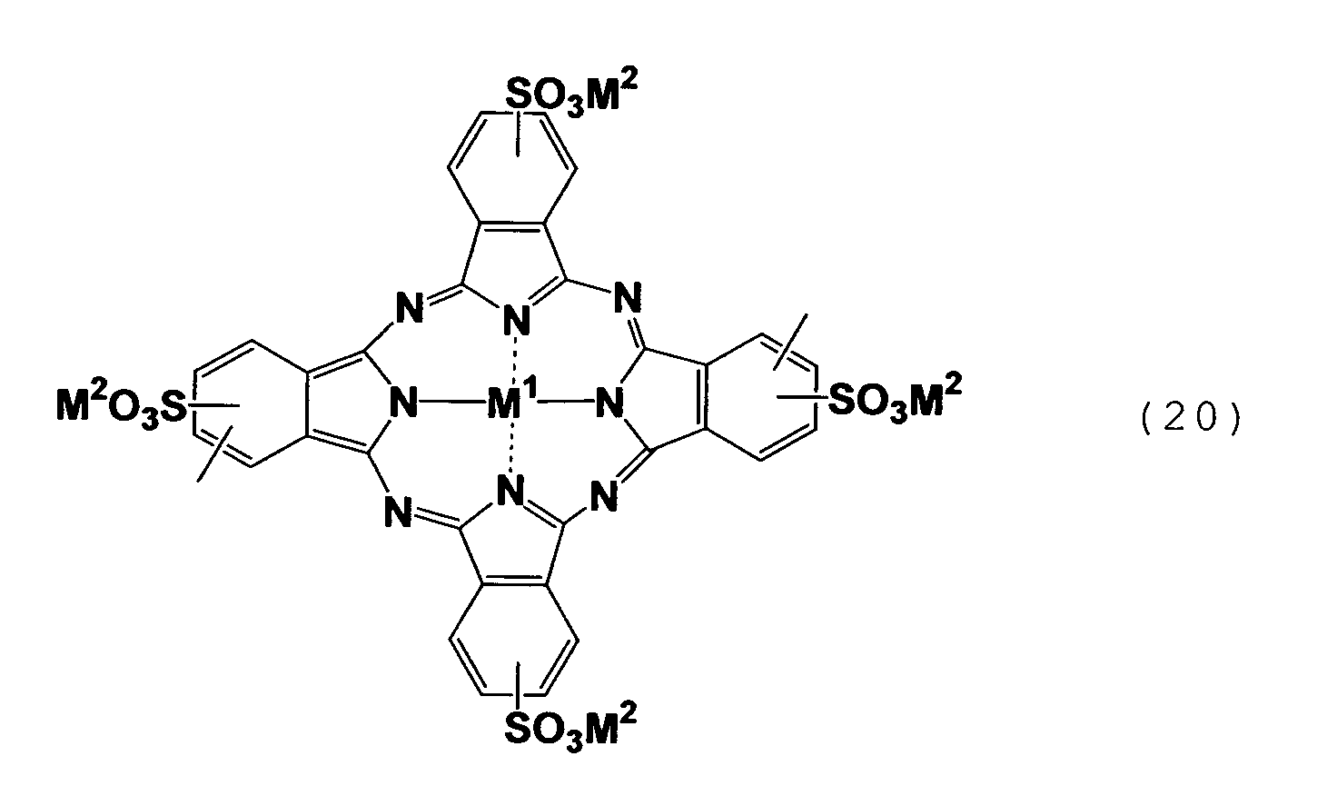
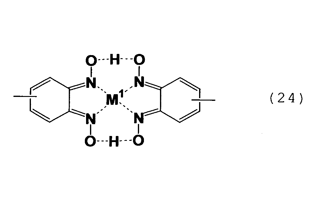
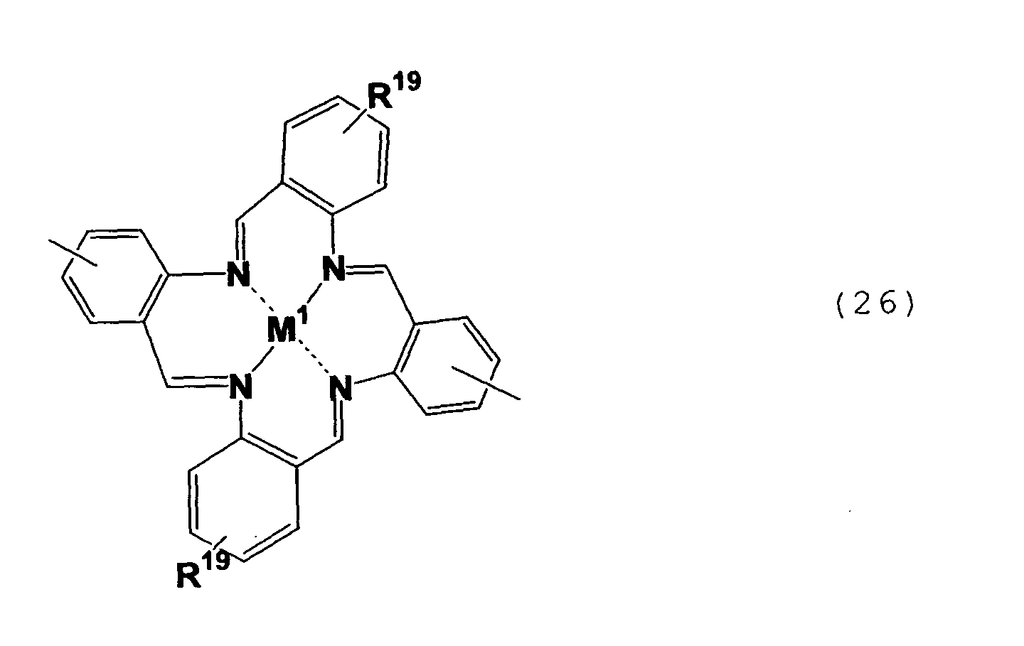
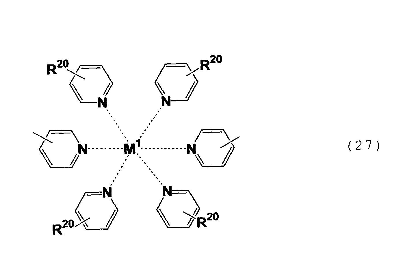
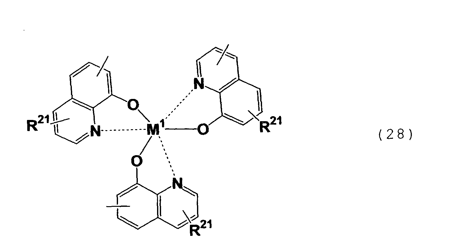
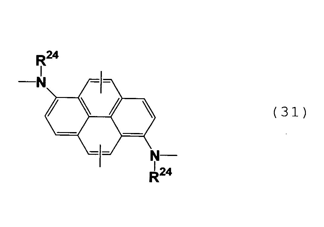
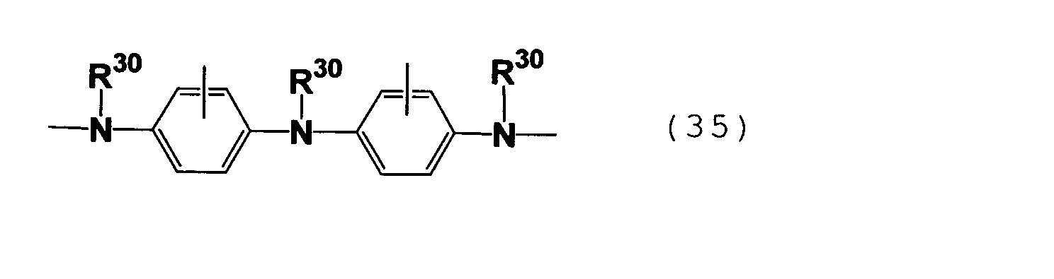
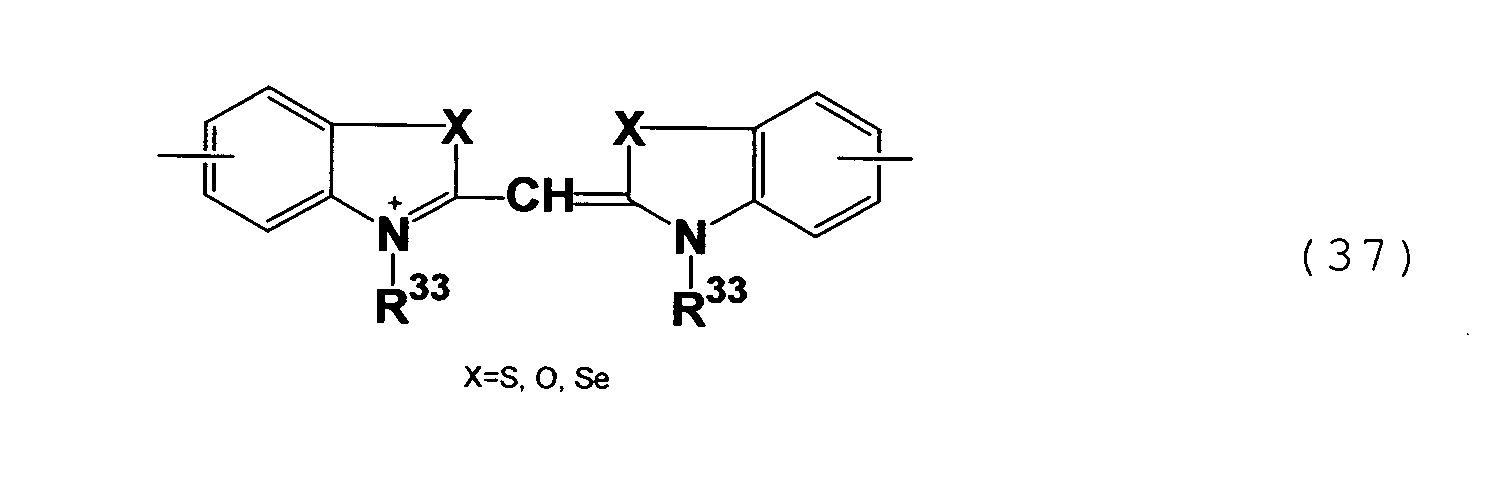
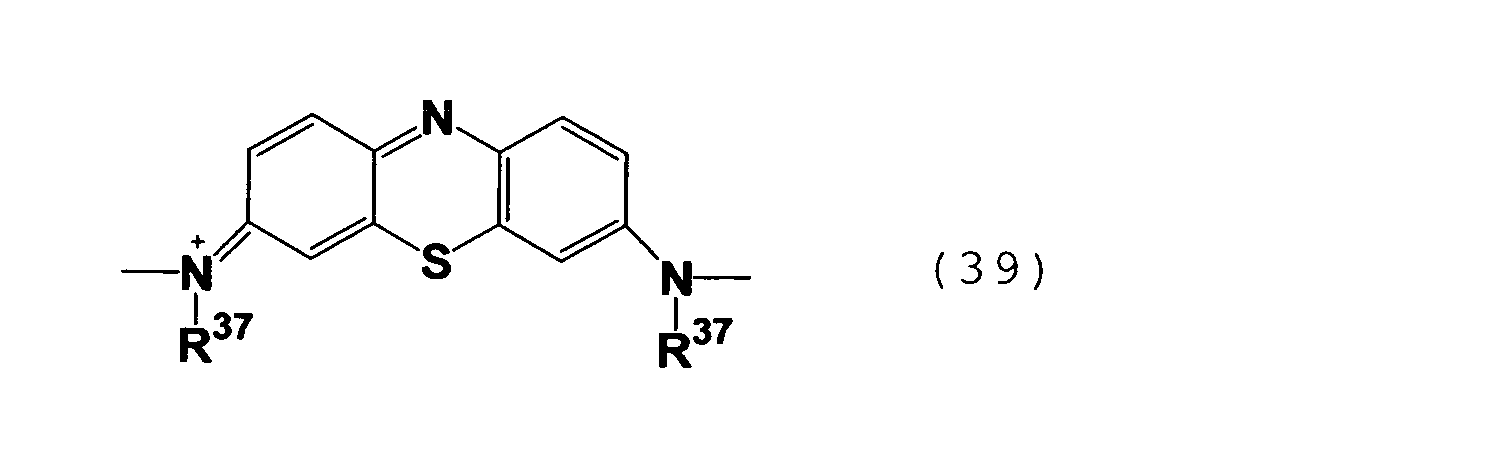
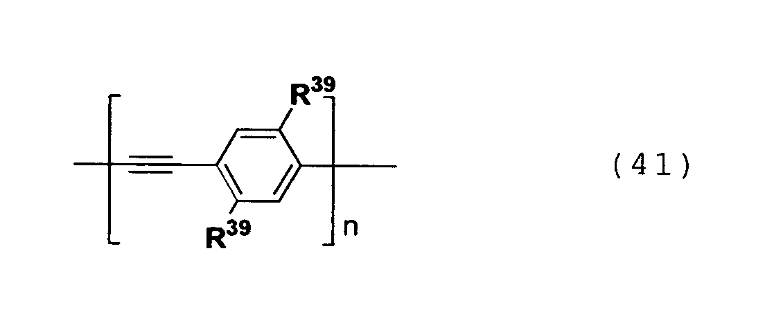
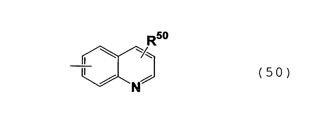
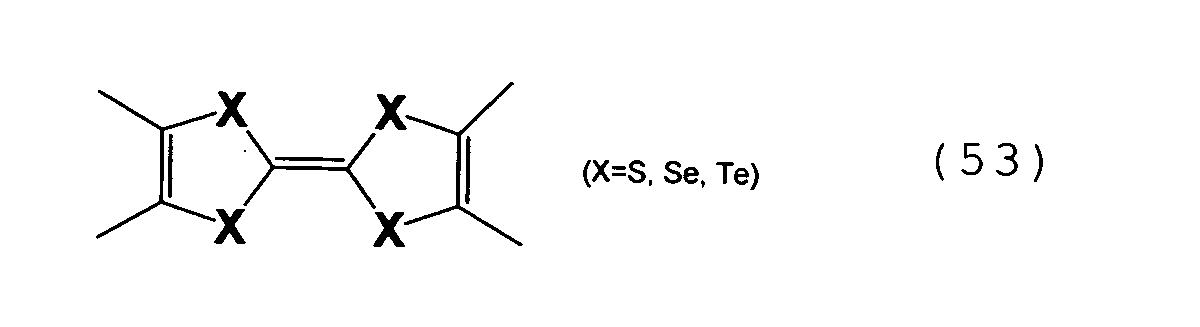
- molecular structures having electron-accepting properties include those represented by formulas (1) to (18) below, while specific examples of the molecular structures having electron-donating properties include those represented by formulas (19) to (61) below:
- R 6 to R 60 may be the same or different from each other and are each independently hydrogen; a straight-chain or branched alkyl, alkenyl or alkoxyl group each having 1 to 10 carbon atoms; or an aryl, aralkyl, or aryloxy group having 6 to 12 carbon atoms.
- R 44 may bond to a cyclopentadienyl ring so as to form a ring or may form a group crosslinking cyclopentadienyl rings which are different from each other.
- R 10 and R 12 may the same or different from each other and are each independently hydrogen, halogen, a cyano, nitro, hydroxyl, amino, carboxyl, acetyl, or formyl group, a straight-chain or branched alkyl, alkenyl, alkoxyl, alkylthio or alkyloxycarbonyl group having 1 to 10 carbon atoms, or an aryl, aralkyl, or aryloxy group having 6 to 12 carbon atoms.
- R 6 to R 60 groups When a plurality of R 6 to R 60 groups exist in one of the formulas they may be the same or different from each other.
- a - and B - may be the same or different from each other and are each independently a counter anion selected from the group consisting of halogen anions, ClO 4 - , BF 4 - , PF 6 - , CH 3 COO - , and CH 3 (C 6 H 4 )SO 3 - .
- n and n are each independently an integer of 1 to 1,000, preferably 2 to 500, and k and 1 indicate the number of each cyclic hydrocarbon group which can be substituted and are each usually an integer of 0 to 4.
- M 1 is a metal atom such as Cu, Zn, Co, Fe, Ti, Mg, Ni, Mo, Os, and Ru.
- M 2 is an alkali metal or alkaline earth metal such as Li, Na, Mg, and Ca.
- M 3 is Cr, Co, Fe, Mg, Ni, Os, Ru, V, X-Hf-Y, X-Mo-Y, X-Nb-Y, X-Ti-Y, X-V-Y or X-Zr-Y wherein X and Y are each independently hydrogen, halogen or an alkyl group having 1 to 12 carbon atoms and may be the same or different from each other.
- alkyl group examples include methyl, ethyl, propyl, i-propyl, butyl, s-butyl, t-butyl, pentyl, isopentyl, neopentyl, t-pentyl, hexyl, isohexyl, heptyl, octyl, nonyl, and decyl groups.
- alkenyl group include vinyl, allyl, isopropenyl, butylenyl, pentylenyl, and hexenyl group.
- alkoxy group examples include methoxy, ethoxy, propoxy, i-propoxy, butoxy, s-butoxy, t-butoxy, pentoxy, isopentoxy, neopentyloxy, t-pentyloxy, hexyloxy, isohexyloxy, heptyloxy, octyloxy, nonyloxy, and decyloxy groups.
- aryl group include phenyl, xylyl, tolyl, cumenyl, and naphthyl groups.
- aralkyl group examples include benzyl and trimethyl.
- the aryloxy group include phenoxy and tolyloxy groups.
- the above-described electron-donating molecular structure and electron-accepting molecular structure chemically bond to each other via covalent bond or ion bond.
- the covalent bond include those by a hydrocarbon group having 1 to 20 and preferably 1 to 10 carbon atoms, specific examples of which include hydrocarbon groups such as alkylene groups, hydrocarbon groups containing an ester bond, hydrocarbon groups containing an ether bond, hydrocarbon groups containing an amide bond, hydrocarbon groups containing a thioether bond, hydrocarbon groups containing an amine bond, hydrocarbon groups containing a urethane bond, and hydrocarbon groups containing a silyl bond.
- Preferred combinations of the electron-accepting molecular structure and the electron-donating molecular structure are a fullerene derivative (formula (3)) and a poly(phenylenevinylene)derivative (formula (40)); a cyano group-containing poly(phenylenevinylene)derivative (formula (4)) and a poly(phenylenevinylene)derivative (formula (40)); a viologen derivative (formula (1)) and an amine derivative (formulas (29) to (35)); a viologen derivative (formula (1)) and a metallocene derivative (formula (46)); a viologen derivative (formula (1)) and a polythiophene derivative (formula (42)); a viologen derivative (formula (1)) and a polypyrrole derivative (formula (42)); a viologen derivative (formula (1)) and a poly(phenylenevinylene)derivative (formula (40));
- R 6 , R 9 , R 10 , R 12 to R 14 , R 16 , and R 38 may be the same or different from each other and are each independently a straight-chain or branched alkyl, alkenyl, or alkoxyl group each having 1 to 10 carbon atoms or an aryl, aralkyl, aryloxy, or aralkyl group each having 6 to 12 carbon atoms.
- R 15 is a divalent hydrocarbon group having 1 to 20 and preferably 1 to 10 carbon atoms.
- a - and B - may be the same or different from each other and are each independently a counter anion selected from the group consisting of halogen anions, ClO 4 - , BF 4 - , PF 6 - , CH 3 COO - , and CH 3 (C 6 H 4 )SO 3 - .
- m and n are each independently an integer of 1 to 1,000 and preferably 2 to 500
- k and 1 indicate the number of each cyclic hydrocarbon group which can be substituted and are each usually an integer of 0 to 4.
- R 15 in formulas (62) to (66) include hydrocarbon groups such as alkylene groups, hydrocarbon groups containing an ester bond, hydrocarbon groups containing an ether bond, hydrocarbon groups containing an amide bond, hydrocarbon groups containing a thioether bond, hydrocarbon groups containing an amine bond, hydrocarbon groups containing a urethane bond, and hydrocarbon groups containing a silyl bond.
- hydrocarbon groups such as alkylene groups, hydrocarbon groups containing an ester bond, hydrocarbon groups containing an ether bond, hydrocarbon groups containing an amide bond, hydrocarbon groups containing a thioether bond, hydrocarbon groups containing an amine bond, hydrocarbon groups containing a urethane bond, and hydrocarbon groups containing a silyl bond.
- hydrocarbon group containing an ester bond examples include those represented by the formulas "-R-COO-R' -" and “-R-OCO-R' -” wherein R and R' are each independently an alkylene group having 1 to 8 carbon atoms.
- hydrocarbon group containing an ether bond examples include those represented by the formula "-R-O-R'-” wherein R and R' are each independently an alkylene group having 1 to 10 carbon atoms.
- hydrocarbon group containing an amide bond examples include those represented by the formulas "-R-CONH-R'-" and "-R-NHCO-R'-” wherein R and R' are each independently an alkylene group having 1 to 8 carbon atoms.
- hydrocarbon group containing a thioether bond examples include those represented by the formula "-R-S-R'-" wherein R and R' are each independently an alkylene group having 1 to 10 carbon atoms.
- hydrocarbon group containing an amine bond examples include those represented by the formulas "-R-NH-R' -" wherein R and R' are each independently an alkylene group having 1 to 10 carbon atoms and "-R-NH-Ph-" wherein R is an alkylene group having 1 to 10 carbon atoms and Ph is an arylene group or substituted arylene group having 6 to 12 carbon atoms.
- hydrocarbon group containing a urethane bond examples include those represented by the formulas "-R-OCONH-R' -" and “-R-NHCOO-R' -” wherein R and R' are each independently an alkylene group having 1 to 8 carbon atoms.
- hydrocarbon group containing a silyl bond examples include those represented by the formula "-R-Si (R") 2 -R'-” wherein R and R' are each independently an alkylene group having 1 to 8 carbon atoms and R" is a methyl or ethyl group.
- R 1 to R 9 and R 13 to R 60 may be the same or different from each other and are each independently hydrogen; a straight-chain or branched alkyl, alkenyl or alkoxyl group each having 1 to 10 carbon atoms; or an aryl, aralkyl, or aryloxy group having 6 to 12 carbon atoms.
- R 44 may be bonded to a cyclopentadienyl ring so as to form a ring or may form a group crosslinking cyclopentadienyl rings which are different from each other.
- R 10 to R 12 may be the same or different from each other and are each independently hydrogen; halogen; cyano, nitro, hydroxyl, amino, carboxyl, acetyl or holmyl group; a straight-chain or branched alkyl, alkenyl, alkoxyl, alkylthio or alkyloxycarbonyl group having 1 to 10 carbon atoms; or an aryl, aralkyl, or aryloxy group having 6 to 12 carbon atoms.
- each R 1 to R 60 groups may be the same or different from each other.
- a - and B - may be the same or different from each other and are each independently a counter anion selected from the group consisting of halogen anions, ClO 4 - , BF 4 - , PF 6 - , CH 3 COO - , and CH 3 (C 6 H 4 )SO 3 - .
- n and n are each independently an integer of 1 to 1,000, preferably 2 to 500, and k and 1 indicate the number of each cyclic hydrocarbon group which can be substituted and are each usually an integer of 0 to 4.
- M 1 is a metal atom such as Cu, Zn, Co, Fe, Ti, Mg, Ni, Mo, Os, and Ru.
- M 2 is an alkali metal or alkaline earth metal such as Li, Na, Mg, and Ca.
- M 3 is Cr, Co, Fe, Mg, Ni, Os, Ru, V, X-Hf-Y, X-Mo-Y, X-Nb-Y, X-Ti-Y, X-V-Y or X-Zr-Y wherein X and Y are each independently hydrogen, halogen or an alkyl group having 1 to 12 carbon atoms and may be the same or different from each other.
- alkyl group examples include methyl, ethyl, propyl, i-propyl, butyl, s-butyl, t-butyl, pentyl, isopentyl, neopentyl, t-pentyl, hexyl, isohexyl, heptyl, octyl, nonyl, and decyl groups.
- alkenyl group include vinyl, allyl, isopropenyl, butylenyl, pentylenyl, and hexenyl group.
- alkoxy group examples include methoxy, ethoxy, propoxy, i-propoxy, butoxy, s-butoxy, t-butoxy, pentoxy, isopentoxy, neopentyloxy, t-pentyloxy, hexyloxy, isohexyloxy, heptyloxy, octyloxy, nonyloxy, and decyloxy groups.
- aryl group include phenyl, xylyl, tolyl, cumenyl, and naphthyl groups.
- aralkyl group examples include benzyl and trimethyl.
- the aryloxy group include phenoxy and tolyloxy groups.
- the compound having an electron-accepting molecular structure and the compound having an electron-donating molecular structure include polyacetylene, polypyrrole, polypyridine, poly-p-phenylene, poly-p-phenylenesulfide, polyphenylenevinylene, poly(2,5-dihexyloxy-1,4-phenylenevinylene), poly(2,5-dioctyloxy-1,4-phenylenevinylene), poly(2-methoxy-5-(2'-ethylhexyloxy)-1,4-phenylenevinylene), and compounds represented by formulas (69) to (131):
- Preferred combinations of an electron-accepting molecular structure and an electron-donating molecular structure are a fullerene derivative (formula (3')) and a poly(phenylenevinylene)derivative (formula (40')); a cyano group-containing poly(phenylenevinylene)derivative (formula (4')) and a poly(phenylenevinylene)derivative (formula (40')); a viologen derivative (formula (1')) and an amine derivative (formulas (29') to (35')); a viologen derivative (formula (1')) and a metallocene derivative (formula (46')); a viologen derivative (formula (1')) and a polythiophene derivative (formula (42')); a viologen derivative (formula (1')) and a polypyrrole derivative (formula (42')); a viologen derivative (formula (1'
- Compounds (A) having both an electron-donating molecular structure and an electron-accepting molecular structure, Compounds (B) having an electron-donating molecular structure and Compounds (C) having an electron-accepting molecular structure to be dispersed in the polymer forming the photoelectric converting layer preferably have electric conductivity. Whether or not these compounds have electric conductivity can be easily determined in a conventional manner. For example, whether or not these compounds have electric conductivity can be determined by measuring the electric conductivity in a conventional manner after the compound are doped.
- the compounds have an electric conductivity of generally 10 -6 to 10 6 S/cm and preferably 10 -4 to 10 5 S/cm.
- the present invention is characterized in that the compound (A) having both an electron-donating molecular structure and an electron-accepting molecular structure and/or the compound (B) having an electron-donating molecular structure and the compound (C) having an electron-accepting molecular structure are dispersed in the polymer forming the photoelectric converting layer.
- the compounds may be dispersed by any method using a homogenizer, a ball mill, a beads mill, a sand mill, a twin roll mill, or a triple roll mill.
- the compounds may be dispersed or dissolved using a suitable solvent to an extent that the present invention is not prevented from achieving the object.
- the polymer precursor may be polymerized so as to be a polymer.
- an electrically conductive substrate on which the photoelectric converting layer is formed is usually produced by laminating a transparent electrode layer on a transparent substrate.
- the material, thickness, size, and shape of the substrate can be properly selected depending on the purposes.
- the substrate may be selected from colored or colorless glasses, wire glasses, glass blocks, and colored or colorless transparent resins.
- polyesters such as polyethylene terephthalate, polyamides, polysulfones, polyethersulfones, polyether ether ketones, polyphenylene sulfides, polycarbonates, polyimides, polymethyl methacrylates, polystyrenes, cellulose triacetates, and polymethyl pentenes.
- transparent used herein denotes a transmissivity of 10 to 100 percent.
- the substrates used herein are those having a smooth surface at ordinary temperature, which surface may be flat or curved or deformed with stress.
- the layer may be a metal film of gold, silver, chromium, copper, or tungsten or an electrically conductive film made of a metal oxide.
- Preferred examples of the metal oxide include tin oxide, zinc oxide, and those obtained by doping thereto trace amounts of components such as Indium Tin Oxide (ITO (In 2 O 3 :Sn)), Fluorine doped Tin Oxide (FTO (SnO 2 :F)), and Aluminum doped Zinc Oxide (AZO (ZnO:Al)).
- the film thickness is usually from 100 to 5,000 nm and preferably from 500 to 3,000 nm.
- the surface resistance (resistivity) is properly selected depending on the use of the substrate in the present invention, but is usually from 0.5 to 500 ⁇ /sq and preferably from 2 to 50 ⁇ /sq.
- the method of forming the transparent electrode layer is properly selected from any conventional methods depending on the type of the above-described metal or metal oxide used as the electrode layer. In general, the method is selected from vacuum deposition, ion plating, CVD, and sputtering. In any of the methods, the transparent electrode layer is desirously formed at a substrate temperature of 20 to 700°C.
- a semiconductor layer may be provided between the electrically conductive substrate and the photoelectric converting layer.
- materials used for producing the semiconductor layer include Bi 2 S 3 , CdS, CdSe, CdTe, CuInS 2 , CuInSe 2 , Fe 2 O 3 , GaP, GaAs, InP, Nb 2 O 5 , PbS, Si, SnO 2 , TiO 2 , WO 3 , ZnO, and ZnS, among which preferred are CdS, CdSe, CuInS 2 , CuInSe 2 , Fe 2 O 3 , GaAs, InP, Nb 2 O 5 , PbS, SnO 2 , TiO 2 , WO 3 , and ZnO. These materials may be used in combination. Particularly preferred are TiO 2 , ZnO, SnO 2 , and Nb 2 O 5 , while most preferred are TiO 2 and ZnO.
- the semiconductor used in the present invention may be monocrystal or polycrystal.
- the crystal system may be selected from those of anatase, rutile, or brookite type among which preferred are those of anatase type.
- the semiconductor layer may be formed by any suitable conventional method.
- the semiconductor layer may be obtained by coating a nanoparticle dispersant or a sol solution, of the above-mentioned semiconductor on the substrate by any conventional method. No particular limitation is imposed on the coating method. Therefore, the coating may be conducted by a method wherein the semiconductor layer is obtained in the form of film by casting; spin-coating; dip-coating; bar-coating; and various printing methods such as screen-printing.
- the thickness of the semiconductor layer may be properly selected but is 0.5 ⁇ m or more and 50 ⁇ m or less and preferably 1 ⁇ m or more and 20 ⁇ m or less.
- the photoelectric converting device of the present invention may be provided with an electron blocking layer and/or a hole transport layer; a hole blocking layer and/or an electron transport layer; or a protection layer.
- the electron blocking layer and/or the hole transport layer are usually arranged between the positive pole and the photoelectric converting layer, while the hole blocking layer and/or the electron transport layer are usually arranged between the negative pole and the photoelectric converting layer.
- Fig. 2 shows an example of the layer structure.
- Materials for forming the electron blocking layer and the hole transport layer may be any materials as long as they have the function to block photogenerated electrons or the function to transport photogenerated holes.
- Specific examples of such materials include electrically conductive polymers such as carbazole derivatives, triazole derivatives, oxazole derivatives, oxadiazole derivatives, imidazole derivatives, polyarylalkane derivatives, pyrazoline derivatives, pyrazolone derivatives, phenylenediamine derivatives, arylamine derivatives, amino-substituted-chalcone derivatives, styrylanthracene derivatives, fluorenone derivatives, hydrazone derivatives, stilbene derivatives, silazane derivatives, aromatic tertiary amine compounds, styrylamine compounds, aromatic dimethylidene-based compounds, porphyrin-based compounds, polysilane-based compounds, poly(N-vinylcarbazole)derivatives, aniline-based copolymers
- the electron blocking layer and/or the hole transport layer may be of a single-layered structure composed of one or more of the materials exemplified above or a multi-layered structure composed of a plurality of layers each having the same or different composition.
- the electron blocking layer and/or the hole transport layer may be formed by a method such as vacuum-deposition, LB method, ink jet method, and a coating method wherein any of the above-mentioned materials is dissolved or dispersed in a solvent and then coated by spin-coating, casting, or dip-coating.
- a method such as vacuum-deposition, LB method, ink jet method, and a coating method wherein any of the above-mentioned materials is dissolved or dispersed in a solvent and then coated by spin-coating, casting, or dip-coating.
- a resin component When coating is used, a resin component may be dissolved or dispersed with any of the above materials thereby preparing a coating solution.
- Eligible resin components are polyvinyl chloride, polycarbonate, polystyrene, polymethylmethacrylate, polybutylmethacrylate, polyester, polysulfone, polyphenyleneoxide, polybutadiene, poly(N-vinylcarbazole), hydrocarbon resins, ketone resins, phenoxy resins, polyamide, ethyl cellulose, polyvinyl acetate, ABS resins, polyurethane, melamine resins, unsaturated polyester resins, alkyd resins, epoxy resins, and silicon resins.
- the thickness of the electron blocking layer and the hole transport layer is preferably from 1 nm to 5 ⁇ m, more preferably from 5 nm to 1 ⁇ m, and particularly preferably from 10 nm to 500 nm.
- Materials for forming the hole blocking layer and the electron transport layer may be any materials as long as they have the function to block photogenerated holes or the function to transport photogenerated electrons.
- Specific examples of such materials include triazole derivatives, oxazole derivatives, oxadiazole derivatives, fluorenone derivatives, anthraquinodimethane derivatives, anthrone derivatives, diphenylquinone derivatives, thiopyrandioxide derivatives, carbodiimide derivatives, fluorenylidene methane derivatives, distyrylpyrazine derivatives, heterocyclic tetracarboxylic anhydrides such as naphthaleneperylene, phthalocyanine derivatives, and metal complexes such as those of 8-quinolinol derivatives and those having metal phthalocyanine, benzoxazole or benzothiazole as a ligand.
- the hole blocking layer and/or the electron transport layer may be of a single-layered structure composed of one or more of the materials exemplified above or a multi-layered structure composed of a plurality of layers each having the same or different composition.
- the hole blocking layer and/or the electron transport layer may be formed by a method such as vacuum-deposition, LB method, ink jet method, and a coating method wherein any of the above-mentioned materials is dissolved or dispersed in a solvent and then coated by spin-coating, casting, or dip-coating.
- a method such as vacuum-deposition, LB method, ink jet method, and a coating method wherein any of the above-mentioned materials is dissolved or dispersed in a solvent and then coated by spin-coating, casting, or dip-coating.
- a resin component When coating is used, a resin component may be dissolved or dispersed with any of the above materials thereby preparing a coating solution.
- Eligible resin components are the same as those exemplified with respect to the electron blocking layer and/or the hole transport layer. No particular limitation is imposed on the thickness of the hole blocking layer and/or the electron transport layer. However, the thickness is preferably from 1 nm to 5 ⁇ m, more preferably from 5 nm to 1 ⁇ m, and particularly preferably from 10 nm to 500 nm.
- the protection layer has a function to prevent objects such as moisture and oxygen facilitating deterioration of the device from entering thereinto.
- Eligible materials for the protection layer are metals such as In, Sn, Pb, Au, Cu, Ag, Al, Ti, and Ni; metal oxides such as MgO, SiO, SiO 2 , Al 2 O 3 , GeO, NiO, CaO, BaO, Fe 2 O 3 , Y 2 O 3 , and TiO 2 ; metal fluorides such as MgF 2 , LiF, AlF 3 , and CaF 2 ; polyethylene; polypropylene, polymethylmethacrylate; polyimide; polyurea; polytetrafluoroethylene; polychlorotrifluoroethylene; polydichlorofluoroethylene; copolymers of chlorotrifluoroethylene and dichlorodifluoroethylene; copolymers obtained by copolymerizing a monomer mixture containing tetrafluoroethylene and at least one type of
- the protective layer may be formed by any method such as sputtering, reactive sputtering, MBE (molecular beam epitaxy), cluster ion beam, ion plating, plasma polymerization (high-frequency excitation ion plating), plasma CVD, laser CVD, thermal CVD, gas source CVD, coating, and ink jet.
- the electrically conductive film formed on the photoelectric converting layer may be formed from a metal such as aluminum, magnesium, gold, silver, platinum, indium, copper, and chromium, an alloy of magnesium and silver, an electrically conductive carbon, or a metal paste of silver, gold, or copper.
- a metal such as aluminum, magnesium, gold, silver, platinum, indium, copper, and chromium, an alloy of magnesium and silver, an electrically conductive carbon, or a metal paste of silver, gold, or copper.
- the method of forming the electrically conductive film is properly selected from conventional methods depending on the type of the above-exemplified materials.
- conventional methods include dry filming such as vacuum deposition, ion-plating, CVD, and sputtering; spin-coating; dip-coating; bar-coating; dispensing; and various printing methods such as screen-printing.
- the film thickness is usually from 100 to 5,000 ⁇ m, preferably from 500 to 3,000 ⁇ m.
- the surface resistance (resistivity) is properly selected depending on the use of the photoelectric converting device of the present invention but is usually from 0.5 to 500 ⁇ /sq and preferably from 2 to 50 ⁇ /sq.
- the photoelectric converting device of the present invention may be in the form of a laminate of a counter electrode substrate, the photoelectric converting layer comprising the compound (A) having both an electron donating molecular structure and an electron accepting molecular structure and/or the compound (B) having an electron donating molecular structure and the compound (C) having an electron accepting molecular structure dispersed in the polymer, and the electrically conductive substrate.
- Examples of the counter electrode substrates include supporting substrates having electric conductivity per se and those obtained by forming an electrically conductive film on supporting substrates.
- the supporting substrate may or may not have electrical conductivity and may be selected from metals such as gold and platinum, colored or colorless glasses, wire glasses, glass blocks, and colored or colorless transparent resins.
- Specific examples include polyesters such as polyethylene terephthalate, polyamides, polysulfones, polyethersulfones, polyether ether ketones, polyphenylene sulfides, polycarbonates, polyimides, polymethyl methacrylates, polystyrenes, cellulose triacetates, and polymethyl pentenes.
- the substrates used herein are those having a smooth surface at ordinary temperature, which surface may be flat or curved or deformed with stress.
- the counter electrode substrates can be obtained by forming a film of a metal such as gold or platinum, In 2 O 3 :Sn, SnO 2 :F, ZnO:Al by a conventional method such as vacuum-deposition, electron beam vacuum deposition, or sputtering.
- an electrolyte layer may be provided between the photoelectric converting layer and the counter electrode substrate.
- the electrolyte layer is an ion conductive material film containing at least one or more substances selected from (a) polymeric matrixes, (b) plasticizers, and (c) supporting electrolytes and exhibits reversible oxidation-reduction properties by (a) to (c) above or (d) redox agents.
- polymeric compounds exhibiting properties of the above-described polymeric matrix include homopolymers and copolymers of hexafluoropropylene, tetrafluoroethylene, trifluoroethylene, ethylene, propylene, acrylonitrile, vinylidene chloride, acrylic acid, methacrylic acid, methyl acrylate, ethyl acrylate, methyl methacrylate, and styrene polyfluorovinylidene. These polymers may be used individually or in combination.
- the plasticizer may be any plasticizers as long as they are solvents which are generally used for electrochemical cells or electric cells. Specific examples are acetic anhydride, methanol, ethanol, tetrahydrofuran, propylene carbonate, nitromethane, acetonitrile, dimethylformamide, dimethylsulfoxide, hexamethylphosphoamide, ethylene carbonate, dimethoxyethane, ⁇ -butyrolactone, ⁇ -valerolactone, sulfolane, propionnitrile, glutaronitrile, tetrahydrofuran, adiponitrile, methoxyacetonitrile, dimethylacetoamide, methylpyrrolidinone, dioxolane, trimethyl phosphate, triethyl phosphate, tripropyl phosphate, ethyldimethyl phosphate, tributyl phosphate, tripentyl phosphate, trihexyl phosphate, triheptyl
- Particularly preferred examples include propylene carbonate, ethylene carbonate, dimethylsulfoxide, dimethoxyethane, acetonitrile, ⁇ -butyrolactone, sulfolane, dioxolane, dimethylformamide, tetrahydrofuran, adiponitrile, methoxyacetonitrile, dimethylacetoamide, methylpyrrolidinone, trimethyl phosphate, and triethyl phosphate.
- plasticizers may be used alone or in combination.
- the supporting electrolyte may be salts, acids, alkalis, ordinary-temperature melting salts which are generally used in the field of electrochemistry or electric cells.
- the salts may be inorganic ion salts such as alkali metal salts and alkaline earth metal salts, quaternary ammonium salts, cyclic quaternary ammonium salts, and quaternary phosphonium salts. Particularly preferred are Li salts.
- the salts include Li, Na, and K salts having a counter anion selected from halogen ions, SCN - , ClO 4 - , BF 4 - , CF 3 SO 3 - , (CF 3 SO 2 ) 2 N - , (C 2 F 5 SO 2 ) 2 N - , PF 6 - , AsF 6 - , CH 3 COO - , CH 3 (C 6 H 4 )SO 3 - , and (C 2 F 5 SO 2 ) 3 C - .
- halogen ions SCN - , ClO 4 - , BF 4 - , CF 3 SO 3 - , (CF 3 SO 2 ) 2 N - , (C 2 F 5 SO 2 ) 2 N - , PF 6 - , AsF 6 - , CH 3 COO - , CH 3 (C 6 H 4 )SO 3 - , and (C 2 F 5 SO 2 ) 3 C - .
- the salts may be any of quaternary ammonium salts having a counter anion selected from halogen ions, SCN - , ClO 4 - , BF 4 - , CF 3 SO 3 - , (CF 3 SO 2 ) 2 N - , (C 2 F 5 SO 2 ) 2 N - , PF 6 - , AsF 6 - , CH 3 COO - , CH 3 (C 6 H 4 )SO 3 - , and (C 2 F 5 SO 2 ) 3 C - , more specifically (CH 3 ) 4 NBF 4 , (C 2 H 5 ) 4 NBF 4 , (n-C 4 H 9 ) 4 NBF 4 , (C 2 H 5 ) 4 NBr, (C 2 H 5 ) 4 NClO 4 , (n-C 4 H 9 ) 4 NClO 4 , CH 3 (C 2 H 5 ) 3 NBF 4 , (CH 3 ) 2 (C 2 H 5 ) 2 NBF
- the acids which, therefore, may be inorganic acids or organic acids.
- Specific examples of the acids are sulfuric acid, hydrochloric acid, phosphoric acids, sulfonic acids, and carboxylic acids.
- alkalis which, therefore, may be sodium hydroxide, potassium hydroxide, and lithium hydroxide.
- ordinary-temperature melting salt denotes a salt comprising only ion pairs without solvent components, in a melted state (liquid state) at ordinary temperature, more specifically a salt comprising ion pairs which has a melting point of 20°C or below and will be in a liquid state at a temperature exceeding 20°C .
- the ordinary-temperature melting salt may be used alone or in combination.
- Examples of the ordinary-temperature melting salt include those represented by the following formulas: wherein R is an alkyl group having 2 to 20, preferably 2 to 10 carbon atoms and X - is a counter anion selected from halogen ions, SCN - , ClO 4 - , BF 4 - , (CF 3 SO 2 ) 2 N - , (C 2 F 5 SO 2 ) 2 N - , PF 6 - , AsF 6 - , CH 3 COO - , CH 3 (C 6 H 4 )SO 3 - , and (C 2 F 5 SO 2 ) 3 C - ; wherein R1 and R2 are each independently an alkyl group having 1 to 10 carbon atoms, preferably methyl or ethyl or an aralkyl group having 7 to 20, preferably 7 to 13 carbon atoms, preferably benzyl and may be the same or different from each other and X - is a counter anion selected from halogen ions, SCN
- the supporting electrolyte may be contained in the electrolyte layer in an amount of usually 0.1 percent by mass or more, preferably 1 percent by mass or more, and more preferably 10 percent by mass or more and 70 percent by mass or less, preferably 60 percent by mass or less, and more preferably 50 percent by mass or less.
- the redox agents are those enabling a reversible electrochemical oxidation-reduction reaction and are not limited in type.
- the redox agent may be only either one of an oxidant or a reductant or a mixture thereof mixed at a suitable molar ratio.
- a respective oxidation-reduction pair of the polymeric matrix, plasticizer, or supporting electrolyte may be added such that the polymeric matrix, plasticizer, or supporting electrolyte exhibits an electrochemical response.
- the materials capable of making polymeric matrix, plasticizer, or supporting electrolyte exhibit such properties include metallocenium salts such as ferrocenium having a counter anion selected from halogen ions, SCN - , ClO 4 - , BF 4 - , CF 3 SO 3 - , (CF 3 SO 2 ) 2 N - , (C 2 F 5 SO 2 ) 2 N - , PF 6 - , AsF 6 - , CH 3 COO - , CH 3 (C 6 H 4 )SO 3 - , and (C 2 F 5 SO 2 ) 3 C - and halogens such as iodine, bromine, and chlorine.
- the electrolyte layer used in the present invention may contain another component.
- the component include ultraviolet absorbing agents.
- typical examples of the ultraviolet absorbing agents include organic ultraviolet absorbing agents such as compounds having a benzotriazole molecule structure or a benzophenone molecule structure.
- R 81 is hydrogen, halogen or an alkyl group having 1 to 10, preferably 1 to 6 carbon atoms.
- the halogen are fluorine, chlorine, bromine, and iodine.
- the alkyl group include methyl, ethyl, propyl, i-propyl, butyl, t-butyl and cyclohexyl groups.
- R 81 is usually substituted at the 4- or 5-position of the benzotriazole ring but the halogen atom and the alkyl group are usually located at the 4-position.
- R 82 is hydrogen or an alkyl group having 1 to 10, preferably 1 to 6 carbon atoms.
- alkyl group examples include methyl, ethyl, propyl, i-propyl, butyl, t-butyl, and cyclohexyl groups.
- R 83 is an alkylene or alkylidene group having 1 to 10, preferably 1 to 3 carbon atoms. Examples of the alkylene group include methylene, ethylene, trimethylene, and propylene groups. Examples of the alkylidene group include ethylidene and propylidene groups.
- Specific examples of the compounds represented by formula (132) include 3-(5-chloro-2H-benzotriazole-2-yl)-5-(1,1-dimethylethyl)-4-hydroxy-benzene propanoic acid, 3-(2H-benzotriazole-2-yl)-5-(1,1-dimethylethyl)-4-hydroxy-benzene ethanoic acid, 3-(2H-benzotriazole-2-yl)-4-hydroxybenzene ethanoic acid, 3-(5-methyl-2H-benzotriazole-2-yl)-5-(1-methylethyl )-4-hydroxybenzene propanoic acid, 2-(2'-hydroxy-5'-methylphenyl)benzotriazole, 2- [2' -hydroxy-3',5'-bis ( ⁇ , ⁇ -dimethylbenzyl) phenyl] benzotriazole, 2-(2'-hydroxy-3', 5'-di-t-butylphenyl)benz
- R 92 , R 93 , R 95 , R 96 , R 98 , and R 99 may be the same or different from each other and are each independently a hydroxyl group or an alkyl or alkoxy group having 1 to 10, preferably 1 to 6 carbon atoms.
- alkyl group include methyl, ethyl, propyl, i-propyl, butyl, t-butyl, and cyclohexyl groups.
- Specific examples of the alkoxy group are methoxy, ethoxy, propoxy, i-propoxy, and butoxy groups.
- R 91 , R 94 , and R 97 are each independently an alkylene or alkylidene group having 1 to 10, preferably 1 to 3 carbon atoms.
- alkylene group include methylene, ethylene, trimethylene, and propylene groups.
- alkylidene group include ethylidene and propylidene groups.
- p1, p2, p3, q1, q2, and q3 are each independently an integer of 0 to 3.
- Preferred examples of the compounds having a benzophenone molecule structure include 2-hydroxy-4-methoxybenzophenone-5-carboxylic acid, 2,2'-dihydroxy-4-methoxybenzophenone-5-carboxylic acid, 4-(2-hydroxybenzoyl)-3-hydroxybenzen propanoic acid, 2,4-dihydroxybenzophenone, 2-hydroxy-4-methoxybenzophenone, 2-hydroxy-4-methoxybenzophenone-5-sulfonic acid, 2-hydroxy-4-n-octoxybenzophenone, 2,2'-dihydroxy-4,4'-dimethoxybenzophenone, 2,2',4,4'-tetrahydroxybenzophenone, and 2-hydroxy-4-methoxy-2'-carboxybenzophenone.
- ultraviolet absorbing agents may be used in combination.
- the use of the ultraviolet absorbing agent is optional. No particular limitation is imposed on the amount of the ultraviolet absorbing agent to be used. However, if the agent is used, it may be contained in the electrolyte layer in an amount of 0.1 percent by mass or more and preferably 1 percent by mass or more, and 20 percent by mass or less and preferably 10 percent by mass or less.
- the electrolyte layer used in the present invention may be produced as an electrolyte film.
- the method of producing the electrolyte film will be described as follows.
- the electrolyte film used in the present invention can be produced by forming a mixture obtained by blending any of arbitrary components such as a plasticizer, a supporting electrolyte, a redox agent, or an ultraviolet absorbing agent in a polymeric matrix component, into a film in a conventional manner. No particular limitation is imposed on the forming method.
- the film may be formed by extrusion, casting, or spin- or dip-coating.
- Extrusion may be conducted in a conventional manner wherein a polymeric matrix is mixed with any of arbitrary components such as a plasticizer, a supporting electrolyte, a redox agent, an ultraviolet absorbing agent and formed into a film after being heat-melted.
- Casting is conducted by mixing a polymeric matrix with any of arbitrary components such as a plasticizer, a supporting electrolyte, a redox agent, an ultraviolet absorbing agent, adjusting the viscosity of the mixture by adding a suitable diluent, and coating and drying the diluted mixture with a conventional coater normally used for casting thereby forming the mixture into a film.
- a conventional coater normally used for casting thereby forming the mixture into a film.
- the coater include doctor coaters, blade coaters, rod coaters, knife coaters, reverse roll coaters, gravure coaters, spray coaters, and curtain coaters among which a suitable one is selected depending on the viscosity and film thickness.
- Spin coating is conducted by mixing a polymeric matrix with any of arbitrary components such as a plasticizer, a supporting electrolyte, a redox agent, an ultraviolet absorbing agent, adjusting the viscosity of the mixture by adding a suitable diluent, and coating and drying the diluted mixture with a commercially available spin-coater thereby forming the mixture into a film.
- Dip coating is conducted by mixing a polymeric matrix with any of arbitrary components such as a plasticizer, a supporting electrolyte, a redox agent, an ultraviolet absorbing agent, adjusting the viscosity of the mixture by adding a suitable diluent so as to obtain a solution of the mixture, dipping and lifting a suitable substrate therein, and drying the solution thereby forming the mixture into a film.
- the electrolyte film obtained by any of the above-described methods exhibits an ionic conductivity of generally 1 x 10 -7 S/cm or higher, preferably 1 x 10 -6 S/cm or higher, and more preferably 1 x 10 -5 S/cm or higher, at room temperature.
- the ionic conductivity can be determined by a conventional method such as complex impedance method.
- the lower limit is usually 1 ⁇ m or more, preferably 10 ⁇ m or more, while the upper limit is usually 3 mm or less, preferably 1 mm or less.
- the photoelectric converting device of the present invention is suppressed from the phase separation of the photoelectric converting layer and excellent in charge separation efficiency thereby enhancing the light utilizing efficiency and making possible highly efficient solar electric power generation.
- the photoelectric converting device of the present invention can be relatively easily produced and is less in burden to the environment upon production or disposition.
- a 5 cm square ITO glass (a transparent electrically conductive glass obtained by forming an Sn-doped In 2 O 3 film on a glass substrate) with a surface resistance of 10 ⁇ /sq was cleaned by alkali-washing and plasma-ozone washing.
- the coating solution was spin-coated on the ITO glass and dried sufficiently thereby obtaining a photoelectric converting layer.
- the thickness of the layer was about 4.5 ⁇ m. It was confirmed through an observation made on the surface of the layer that the film was uniform and clear.
- the photoelectric converting layer was left standing at a temperature of 80°C for 20 hours, but no particular change was observed.
- a light of a 100 W tungsten lump, uniformed through a diffuser was illuminated from the glass substrate side to the device, and the electric current thereof when the device was short-circuited was measured thereby confirming that a current of 4 ⁇ A was obtained and the device exhibited excellent photoelectric converting properties.
- a 5 cm square ITO glass (a transparent electrically conductive glass obtained by forming an Sn-doped In 2 O 3 film on a glass substrate) with a surface resistance of 10 ⁇ /sq was cleaned by alkali-washing and plasma-ozone washing.
- the coating solution was spin-coated on the ITO glass and dried sufficiently thereby obtaining a photoelectric converting layer.
- the thickness of the layer was about 5 ⁇ m. It was confirmed through an observation made on the surface of the layer that the film was uniform and clear.
- the photoelectric converting layer was left standing at a temperature of 80°C for 20 hours, but no particular change was observed.
- a light of a 100 W tungsten lump, uniformed through a diffuser was illuminated from the glass substrate side to the device, and the electric current thereof when the device was short-circuited was measured thereby confirming that a current of 2.1 ⁇ A was obtained and the device exhibited excellent photoelectric converting properties.
- Polystyrene sulfonate dispersant (manufactured by Bayer Ltd under the name of "Baytron P", solid content : 1.3 %) was spin-coated on a 5 cm square ITO glass (a transparent electrically conductive glass obtained by forming an Sn-doped In 2 O 3 film on a glass substrate) with a surface resistance of 10 ⁇ /sq having been cleaned by alkali-washing and plasma-ozone washing and vacuum-dried at a temperature of 150°C for 2 hours thereby forming a coating layer with a thickness of 100 nm.
- ITO glass a transparent electrically conductive glass obtained by forming an Sn-doped In 2 O 3 film on a glass substrate
- a coating solution obtained by dispersing 200 mg of C 60 as a compound having an electron-accepting molecular structure and 100 mg of Compound (a) used in Example 2 as a compound having an electron-donating molecular structure in a solution obtained by dissolving 500 mg of polymetylmethacrylate (manufactured by FLUKA Ltd., Mw about 200, 000) in 10 g of chloroform.
- the coating solution was dried sufficiently thereby obtaining a photoelectric converting layer.
- the thickness of the layer was about 5 ⁇ m. It was confirmed through an observation made on the surface of the layer that the film was uniform and clear.
- the photoelectric converting layer was left standing at a temperature of 80°C for 20 hours, but no particular change was observed.
- a light of a 100 W tungsten lump, uniformed through a diffuser was illuminated from the glass substrate side to the device, and the electric current thereof when the device was short-circuited was measured thereby confirming that a current of 3.5 ⁇ A was obtained and the device exhibited excellent photoelectric converting properties.
- Polystyrene sulfonate dispersant (manufactured by Bayer Ltd under the name of "Baytron P", solid content : 1.3 %) was spin-coated on a 5 cm square ITO glass (a transparent electrically conductive glass obtained by forming an Sn-doped In 2 O 3 film on a glass substrate) with a surface resistance of 10 ⁇ /sq having been cleaned by alkali-washing and plasma-ozone washing and vacuum-dried at a temperature of 150°C for 2 hours thereby forming a coating layer with a thickness of 100 nm.
- ITO glass a transparent electrically conductive glass obtained by forming an Sn-doped In 2 O 3 film on a glass substrate
- the coating solution was dried sufficiently thereby obtaining a photoelectric converting layer.
- the thickness of the layer was about 5 ⁇ m. It was confirmed through an observation made on the surface of the layer that the film was uniform and clear.
- the photoelectric converting layer was left standing at a temperature of 80°C for 20 hours, but no particular change was observed.
- a light of a 100 W tungsten lump, uniformed through a diffuser was illuminated from the glass substrate side to the device, and the electric current thereof when the device was short-circuited was measured thereby confirming that a current of 4.2 ⁇ A was obtained and the device exhibited excellent photoelectric converting properties.
- Polystyrene sulfonate dispersant (manufactured by Bayer Ltd under the name of "Baytron P", solid content : 1.3 %) was spin-coated on a 5 cm square ITO glass (a transparent electrically conductive glass obtained by forming an Sn-doped In 2 O 3 film on a glass substrate) with a surface resistance of 10 ⁇ /sq having been cleaned by alkali-washing and plasma-ozone washing and vacuum-dried at a temperature of 150°C for 2 hours thereby forming a coating layer with a thickness of 100 nm.
- ITO glass a transparent electrically conductive glass obtained by forming an Sn-doped In 2 O 3 film on a glass substrate
- the coating solution was dried sufficiently thereby obtaining a photoelectric converting layer.
- the thickness of the layer was about 5 ⁇ m. It was confirmed through an observation made on the surface of the layer that the film was uniform and clear.
- the photoelectric converting layer was left standing at a temperature of 80°C for 20 hours, but no particular change was observed.
- a light of a 100 W tungsten lump, uniformed through a diffuser was illuminated from the glass substrate side to the device, and the electric current thereof when the device was short-circuited was measured thereby confirming that a current of 4.5 ⁇ A was obtained and the device exhibited excellent photoelectric converting properties.
Landscapes
- Engineering & Computer Science (AREA)
- Chemical & Material Sciences (AREA)
- Materials Engineering (AREA)
- Nanotechnology (AREA)
- Theoretical Computer Science (AREA)
- Crystallography & Structural Chemistry (AREA)
- Physics & Mathematics (AREA)
- Mathematical Physics (AREA)
- Power Engineering (AREA)
- Chemical Kinetics & Catalysis (AREA)
- Electrochemistry (AREA)
- Microelectronics & Electronic Packaging (AREA)
- Hybrid Cells (AREA)
- Photovoltaic Devices (AREA)
- Electroluminescent Light Sources (AREA)
Abstract
Photoelectric converting devices used for
photovoltaic power generation or a photovoltaic power
generating system have a photoelectric converting
layer comprising an organic compound (A) having both
an electron donating molecular structure and an
electron accepting molecular structure dispersed in
the polymer and/or an organic compound (B) having an
electron donating molecular structure and an organic
compound (C) having an electron accepting molecular
structure, dispersed in a polymer. The photoelectric
converting devices are suppressed in the phase
separation of the photoelectric converting layer and
thus is enhanced in light utilizing efficiency.
Description
The present invention relates to photoelectric
converting devices useful for photovoltaic generators
or photovoltaic generating systems.
In recent years, due to an increased awareness of
environmental issues, attention has been attracted to
solar energy which is an inexpensive and clean energy
source as an alternative for fossil fuels causing
carbon dioxide emission having an affect on the global
warming. Conversion of solar energy to other energies
such as electric energy is important for the effective
use of solar energy. In this connection, inorganic
semiconductor-type photoelectric generators, such as
silicon have been developed and put to practical use.
However, since such photoelectric generators are
enormous in energy consumption for the production
thereof, it has been desired to develop a photoelectric
converting device which can be produced with a low
energy and cost consumption.
Organic compounds are inexpensive and give less
affect to the environment even though being disposed
by incineration after use. With this background in
view, development of a photoelectric converting device
using organic photoelectric converting substances is
one of the most important energy measures.
Interests to the photoelectric converting device
using organic substances have been increased since the
Tang's converting device exhibited about 1 percent
efficiency in 1986 (C. W. Tang. Appl. Phys. Lett., Vol.
48, pages 183-185, January 13, 1986). Thereafter, the
photoelectric converting efficiency has been improved
year by year. For enhancing the efficiency of the
organic photoelectric converting device, it is
necessary to establish a combination of an
electron-donating organic semiconductor (donor) and an
electron-accepting organic semiconductor (acceptor),
a so-called heterojunction structure. An effective
charge separation occurs in the proximity of the
interface between the donor and the acceptor. Based
on such an idea, for example, U. S. Patent Nos. 5,454,880
and 5, 331, 183 proposed a so-called bulk heterojunction
wherein an electric conductive polymer as a donor and
a fullerene derivative as an acceptor are mixed,
thereby developing a photoelectric converting device
with a higher density donor/acceptor interface,
resulting in an enhanced photoelectric converting
efficiency. Therefore, the key factor in development
of an organic photoelectric converting device in recent
years is how the charge separation interface between
the donor and the acceptor is designed.
For developing a photoelectric converting device
with an enhanced photoelectric converting efficiency,
it is also important to transport efficiently carriers
(electrons, holes) generated after charge separation.
Friend et al. succeeded in establishing a structure
with a high carrier mobility efficiency by using an
electron-donating benzocoronen and an
electron-accepting perylene dye, stacking by
self-organization (Science, Vol. 293, pages 1119-1122,
August 10, 2001). Stacking of π conjugated systems
exhibits a large carrier mobility with respect to the
lamination direction.
However, a strong tendency that molecules are
self-organized causes the molecules of donors and
acceptors to gather with the same ones, respectively
upon production of a photoelectric converting device,
resulting in the possibility of phase separation. When
the separation occurs, a rugged surface is formed on
the photoelectric converting layer, leading to a
reduction of the photoelectric converting efficiency.
The present invention was made in view of the
above-described circumstances and thus relates to a
photoelectric converting material enabling a
production of a photoelectric converting layer
excellent in a capability to suppress the phase
separation and also to a photoelectric converting
device using the photoelectric converting material.
As a result of the studies by the inventors of the
present invention, the present invention was achieved
based on the finding that an photoelectric converting
device with excellent properties that it is suppressed
in the phase separation of the photoelectric converting
layer and thus enhanced in the light utilizing
efficiency can be produced by dispersing a specific
compound in a polymer forming the photoelectric
converting layer.
That is, the present invention relates to a
photoelectric converting device which has a
photoelectric converting layer comprising an organic
compound (A) having both an electron donating molecular
structure and an electron accepting molecular
structure dispersed in a polymer.
The present invention also relates to a
photoelectric converting device which has a
photoelectric converting layer comprising an organic
compound (B) having an electron donating molecular
structure and an organic compound (C) having an
electron accepting molecular structure, dispersed in
a polymer.
The present invention will be described below in
more detail.
First of all, described will be a polymer
constituting the photoelectric converting layer of the
photoelectric converting device of the present
invention. No particular limitation is imposed on the
polymer as long as it can disperse an organic compound
(A) having both an electron donating molecular
structure and an electron accepting molecular
structure (hereinafter referred to as Compound (A))or
both an organic compound (B) having an electron
donating molecular structure (hereinafter referred to
as Compound (B)) and an organic compound (C) having an
electron accepting molecular structure (hereinafter
referred to as Compound (C)). Examples of the polymer
include acrylic polymers such as
polymethylmethacrylate and polyethylacrylate;
polyethers such as polyethylene oxide and
polypropylene oxide; polyesters such as polyethylene
terephthalate; electrically conductive polymer
compounds such as polyphenylene vinylene,
polyacetylene, polythiophene, and polypyrrole. More
preferred among these compounds are electrically
conductive polymer compounds. Preferred electrically
conductive polymer compounds are those having an
electric conductivity of generally 10-6 to 106 S/cm and
more preferably 10-4 to 105 S/cm, at a temperature of
20°C.
No particular limitation is imposed on the
molecular weight of the polymer as long as it can
disperse Compound (A) or Compounds (B) and (C) and can
form a photoelectric converting layer, and thus the
molecular weight is suitably selected. Therefore, the
polymer may be any of those having a molecular weight
of usually 1,000 to 5,000,000, preferably 10,000 to
1,000,000 and more preferably 50,000 to 500,000.
No particular limitation is imposed on the content
of Compound (A) having both an electron donating
molecular structure and an electron accepting
molecular structure as long as the present invention
is not prevented from achieving the object thereof.
However, the content of Compound (A) is usually from
5 to 300 parts by mass, preferably 10 to 100 parts by
mass and more preferably 20 to 80 parts by mass, based
on 100 parts by mass of the polymer.
No particular limitation is imposed on the content
of Compound (B) having an electron donating molecular
structure or Compound (C) having an electron accepting
molecular structure as long as the present invention
is not prevented from achieving the object thereof.
The content of Compound (B) having an electron donating
molecular structure is usually from 5 to 300 parts by
mass, preferably 10 to 100 parts by mass and more
preferably 20 to 80 parts by mass, based on 100 parts
by mass of the polymer while the content of Compound
(C) having an electron accepting molecular structure
is usually from 5 to 300 parts by mass, preferably 10
to 100 parts by mass and more preferably 20 to 80 parts
by mass, based on 100 parts by mass of the polymer. No
particular limitation is imposed on the ratio of
Compound (B) having an electron donating molecular
structure to Compound (C) having an electron accepting
molecular structure. However, the mass ratio between
Compounds (B) and (C) is usually from 10/90 to 90/10
and preferably 20/80 to 80/20.
The term "electron-donating molecular structure"
used herein denotes a structure exhibiting properties
that the molecules are small in ionization potential
and likely to become positive ions per se by supplying
electrons to other molecules, while the term
"electron-accepting molecular structure" denotes a
structure exhibiting properties that the molecules are
large in electron affinity and likely to become
negative ions per se by accepting electrons from other
molecules.
When a compound (A) having both an
electron-donating molecular structure and an
electron-accepting molecular structure is used in the
present invention, the above-described
electron-donating and electron-accepting properties
are determined automatically depending on the relative
relationship between their structures having such
properties in the compound (A). Therefore,
combinations of such structures that fulfill these
properties are arbitrarily selected.
When a compound (B) having an electron-donating
molecular structure is used in combination with a
compound (C) having an electron-accepting molecular
structure, the above-described electron-donating and
electron-accepting properties are determined
automatically depending on the relative relationship
between the compounds to be used. Therefore,
combinations of such compounds that fulfill these
properties are arbitrarily selected.
No particular limitation is imposed on the
molecular structure having electron-donating
properties as long as it has electron-donating
properties in the molecular structure portion.
Examples of the structure include amine, metallocene,
polyarylene vinylene, polyanyline, polythiophene,
polypyrrole and polyamine structures.
No particular limitation is imposed on the
molecular structure having electron-accepting
properties as long as it has electron-accepting
properties in the molecular structure portion.
Examples of the structure include viologen, perylene
and fullerene structures.
Specific examples of the molecular structures
having electron-accepting properties include those
represented by formulas (1) to (18) below, while
specific examples of the molecular structures having
electron-donating properties include those
represented by formulas (19) to (61) below:

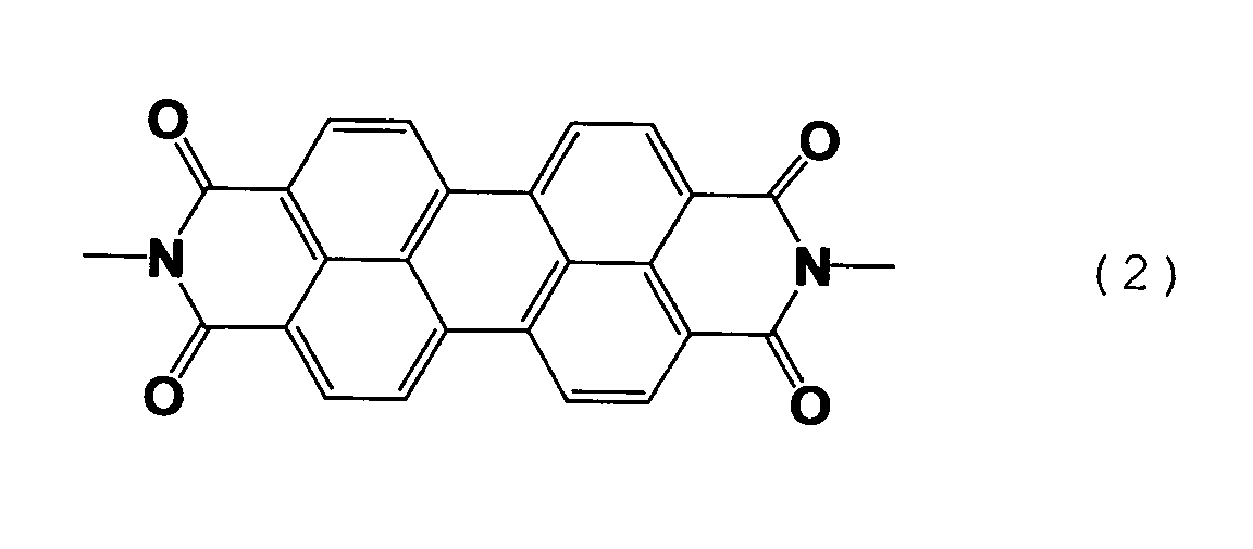
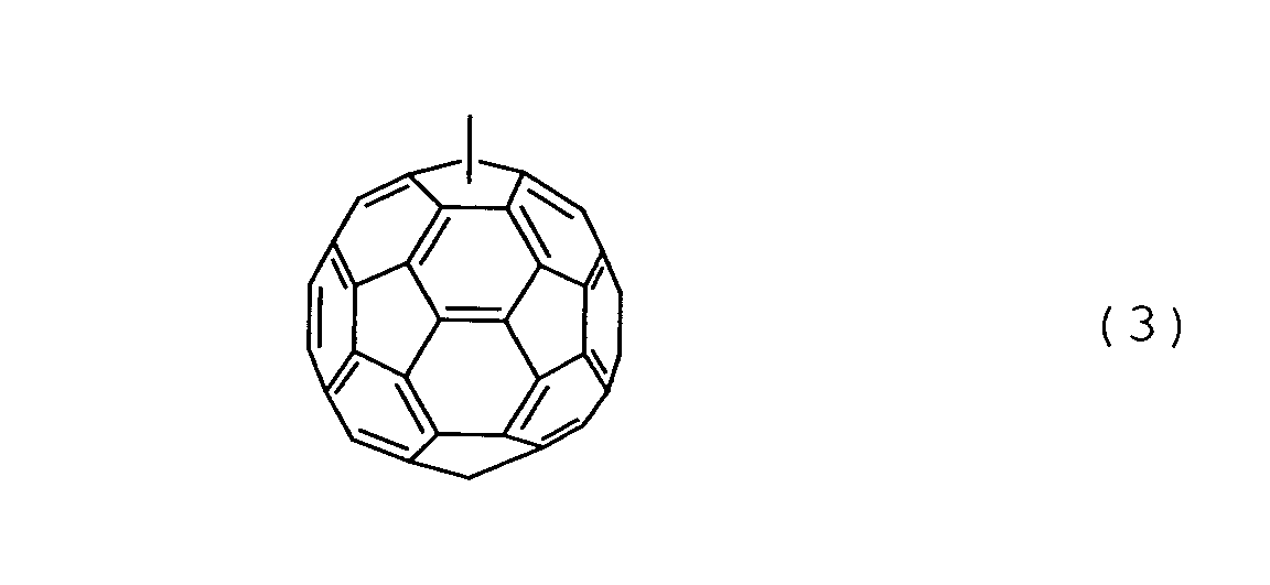


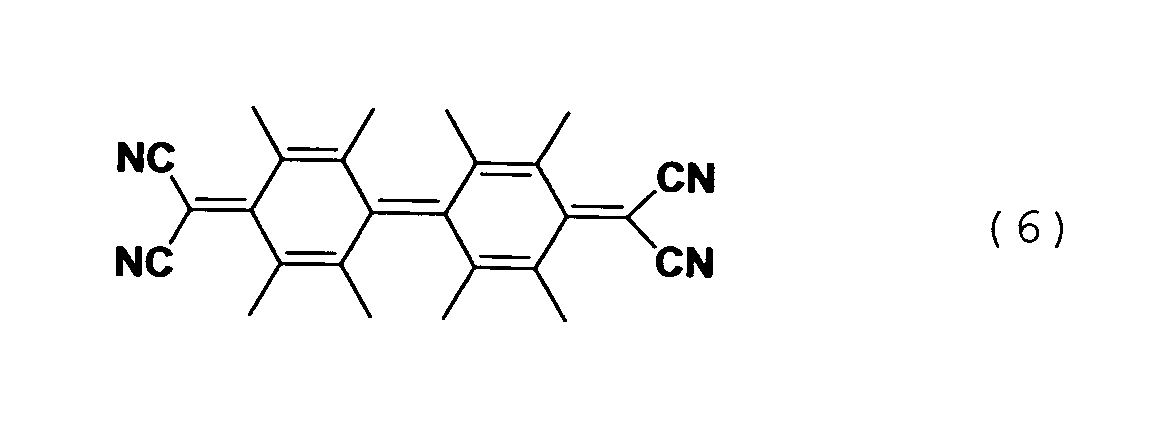


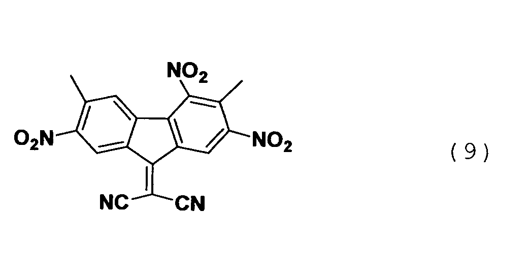




















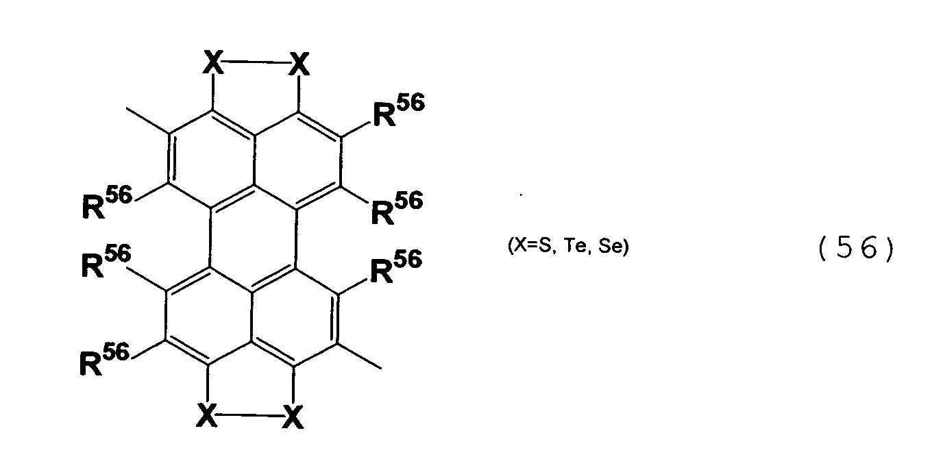


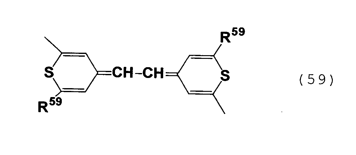
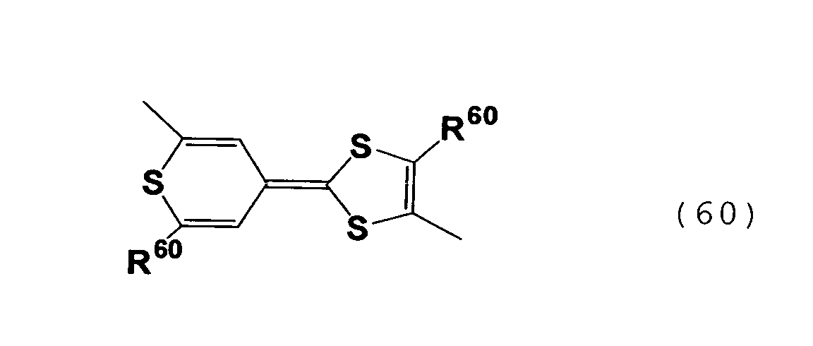

In formulas (1) to (61), R6 to R60 (excluding R10
and R12) may be the same or different from each other
and are each independently hydrogen; a straight-chain
or branched alkyl, alkenyl or alkoxyl group each having
1 to 10 carbon atoms; or an aryl, aralkyl, or aryloxy
group having 6 to 12 carbon atoms. R44 may bond to a
cyclopentadienyl ring so as to form a ring or may form
a group crosslinking cyclopentadienyl rings which are
different from each other.
R10 and R12 may the same or different from each other
and are each independently hydrogen, halogen, a cyano,
nitro, hydroxyl, amino, carboxyl, acetyl, or formyl
group, a straight-chain or branched alkyl, alkenyl,
alkoxyl, alkylthio or alkyloxycarbonyl group having 1
to 10 carbon atoms, or an aryl, aralkyl, or aryloxy group
having 6 to 12 carbon atoms.
When a plurality of R6 to R60 groups exist in one
of the formulas they may be the same or different from
each other.
A- and B- may be the same or different from each
other and are each independently a counter anion
selected from the group consisting of halogen anions,
ClO4 -, BF4 -, PF6 -, CH3COO-, and CH3(C6H4)SO3 -.
In the above formulas, m and n are each
independently an integer of 1 to 1,000, preferably 2
to 500, and k and 1 indicate the number of each cyclic
hydrocarbon group which can be substituted and are each
usually an integer of 0 to 4.
M1 is a metal atom such as Cu, Zn, Co, Fe, Ti, Mg,
Ni, Mo, Os, and Ru. M2 is an alkali metal or alkaline
earth metal such as Li, Na, Mg, and Ca. M3 is Cr, Co,
Fe, Mg, Ni, Os, Ru, V, X-Hf-Y, X-Mo-Y, X-Nb-Y, X-Ti-Y,
X-V-Y or X-Zr-Y wherein X and Y are each independently
hydrogen, halogen or an alkyl group having 1 to 12 carbon
atoms and may be the same or different from each other.
Examples of the alkyl group include methyl, ethyl,
propyl, i-propyl, butyl, s-butyl, t-butyl, pentyl,
isopentyl, neopentyl, t-pentyl, hexyl, isohexyl,
heptyl, octyl, nonyl, and decyl groups. Examples of
the alkenyl group include vinyl, allyl, isopropenyl,
butylenyl, pentylenyl, and hexenyl group. Examples of
the alkoxy group include methoxy, ethoxy, propoxy,
i-propoxy, butoxy, s-butoxy, t-butoxy, pentoxy,
isopentoxy, neopentyloxy, t-pentyloxy, hexyloxy,
isohexyloxy, heptyloxy, octyloxy, nonyloxy, and
decyloxy groups. Examples of the aryl group include
phenyl, xylyl, tolyl, cumenyl, and naphthyl groups.
Examples of the aralkyl group include benzyl and
trimethyl. Examples of the aryloxy group include
phenoxy and tolyloxy groups.
In the compound having both an electron-donating
molecular structure and an electron-accepting
molecular structure, the above-described
electron-donating molecular structure and
electron-accepting molecular structure chemically
bond to each other via covalent bond or ion bond.
Examples of the covalent bond include those by a
hydrocarbon group having 1 to 20 and preferably 1 to
10 carbon atoms, specific examples of which include
hydrocarbon groups such as alkylene groups,
hydrocarbon groups containing an ester bond,
hydrocarbon groups containing an ether bond,
hydrocarbon groups containing an amide bond,
hydrocarbon groups containing a thioether bond,
hydrocarbon groups containing an amine bond,
hydrocarbon groups containing a urethane bond, and
hydrocarbon groups containing a silyl bond.
Preferred combinations of the electron-accepting
molecular structure and the electron-donating
molecular structure are a fullerene derivative
(formula (3)) and a poly(phenylenevinylene)derivative
(formula (40)); a cyano group-containing
poly(phenylenevinylene)derivative (formula (4)) and a
poly(phenylenevinylene)derivative (formula (40)); a
viologen derivative (formula (1)) and an amine
derivative (formulas (29) to (35)); a viologen
derivative (formula (1)) and a metallocene derivative
(formula (46)); a viologen derivative (formula (1)) and
a polythiophene derivative (formula (42)); a viologen
derivative (formula (1)) and a polypyrrole derivative
(formula (42)); a viologen derivative (formula (1)) and
a poly(phenylenevinylene)derivative (formula (40)); a
perylene derivative (formula (2)) and a copper
phthalocyanine derivative (formulas (20) to (22)); a
perylene derivative (formula (2)) and a phthalocyanine
derivative (formula (19)); a perylene derivative
(formula (2)) and an amine derivative (formulas (29)
to (35)); a perylene derivative (formula (2)) and a
poly(phenylenevinylene)derivative (formula (40)); a
perylene derivative (formula (2)) and a polythiophene
derivative (formula (42)); a perylene derivative
(formula (2)) and a polypyrrole derivative (formula
(42)); a perylene derivative (formula (2)) and a
metallocene derivative (formula (46)); a fullerene
derivative (formula (3)) and a copper phthalocyanine
derivative (formulas (20) to (22)); a fullerene
derivative (formula (3)) and an amine derivative
(formulas (29) to (35)); a fullerene derivative
(formula (3)) and a polythiophene derivative (formula
(42)); a fullerene derivative (formula (3)) and a
polypyrrole derivative (formula (42)); a fullerene
derivative (formula (3)) and a metallocene derivative
(formula (46)); a cyano group-containing
poly(phenylenevinylene)derivative (formula (4)) and
an amine derivative (formulas (29) to (35)); a cyano
group-containing poly(phenylenevinylene)derivative
(formula (4)) and a copper phthalocyanine derivative
(formulas (20) to (22)); a cyano group-containing
poly(phenylenevinylene)derivative (formula (4)) and a
polythiophene derivative (formula (42)); a cyano
group-containing poly(phenylenevinylene)derivative
(formula (4)) and a polypyrrole derivative (formula
(42)); and a cyano group-containing
poly(phenylenevinylene)derivative (formula (4)) and a
metallocene group (formula (46)).
Examples of compounds containing such
combinations include those represented by formulas
(62) to (66) given below:


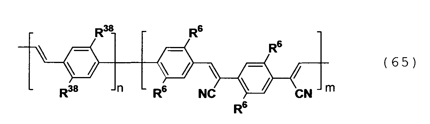
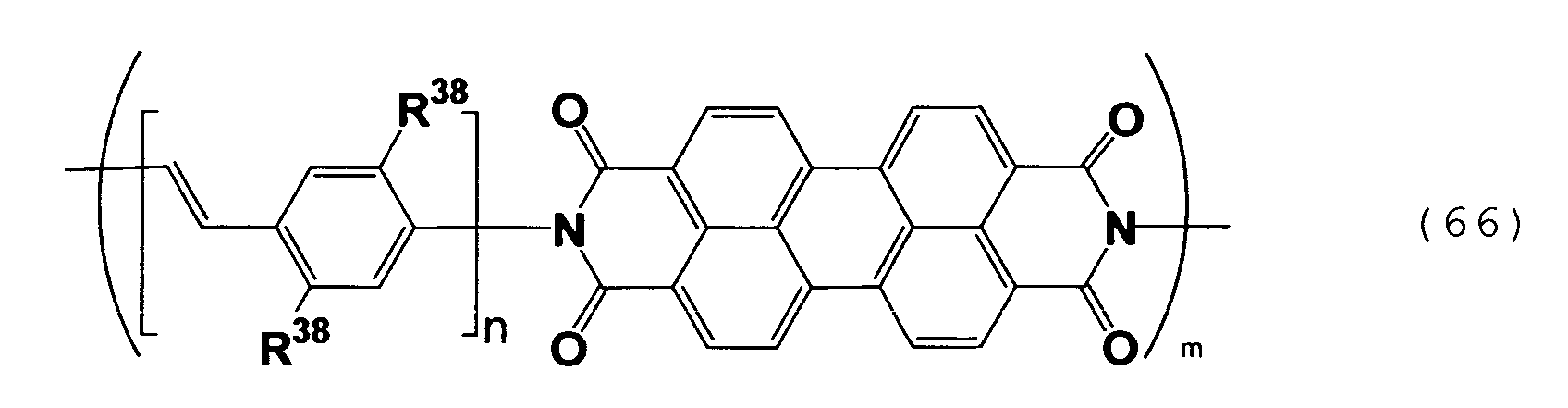
In formulas (62) to (66), R6, R9, R10, R12 to R14,
R16, and R38 may be the same or different from each other
and are each independently a straight-chain or branched
alkyl, alkenyl, or alkoxyl group each having 1 to 10
carbon atoms or an aryl, aralkyl, aryloxy, or aralkyl
group each having 6 to 12 carbon atoms. R15 is a
divalent hydrocarbon group having 1 to 20 and
preferably 1 to 10 carbon atoms. A- and B- may be the
same or different from each other and are each
independently a counter anion selected from the group
consisting of halogen anions, ClO4 -, BF4 -, PF6 -, CH3COO-,
and CH3(C6H4)SO3 -. In the above formulas, m and n are
each independently an integer of 1 to 1,000 and
preferably 2 to 500, and k and 1 indicate the number
of each cyclic hydrocarbon group which can be
substituted and are each usually an integer of 0 to 4.
Specific preferred examples of R15 in formulas
(62) to (66) include hydrocarbon groups such as
alkylene groups, hydrocarbon groups containing an
ester bond, hydrocarbon groups containing an ether bond,
hydrocarbon groups containing an amide bond,
hydrocarbon groups containing a thioether bond,
hydrocarbon groups containing an amine bond,
hydrocarbon groups containing a urethane bond, and
hydrocarbon groups containing a silyl bond.
Examples of the hydrocarbon group containing an
ester bond include those represented by the formulas
"-R-COO-R' -" and "-R-OCO-R' -" wherein R and R' are each
independently an alkylene group having 1 to 8 carbon
atoms. Examples of the hydrocarbon group containing
an ether bond include those represented by the formula
"-R-O-R'-" wherein R and R' are each independently an
alkylene group having 1 to 10 carbon atoms. Examples
of the hydrocarbon group containing an amide bond
include those represented by the formulas
"-R-CONH-R'-" and "-R-NHCO-R'-" wherein R and R' are
each independently an alkylene group having 1 to 8
carbon atoms. Examples of the hydrocarbon group
containing a thioether bond include those represented
by the formula "-R-S-R'-" wherein R and R' are each
independently an alkylene group having 1 to 10 carbon
atoms. Examples of the hydrocarbon group containing
an amine bond include those represented by the formulas
"-R-NH-R' -" wherein R and R' are each independently an
alkylene group having 1 to 10 carbon atoms and
"-R-NH-Ph-" wherein R is an alkylene group having 1 to
10 carbon atoms and Ph is an arylene group or substituted
arylene group having 6 to 12 carbon atoms. Examples
of the hydrocarbon group containing a urethane bond
include those represented by the formulas
"-R-OCONH-R' -" and "-R-NHCOO-R' -" wherein R and R' are
each independently an alkylene group having 1 to 8
carbon atoms. Examples of the hydrocarbon group
containing a silyl bond include those represented by
the formula "-R-Si (R")2-R'-" wherein R and R' are each
independently an alkylene group having 1 to 8 carbon
atoms and R" is a methyl or ethyl group.
Specific preferred examples of these compounds
include those represented by the following formulas:
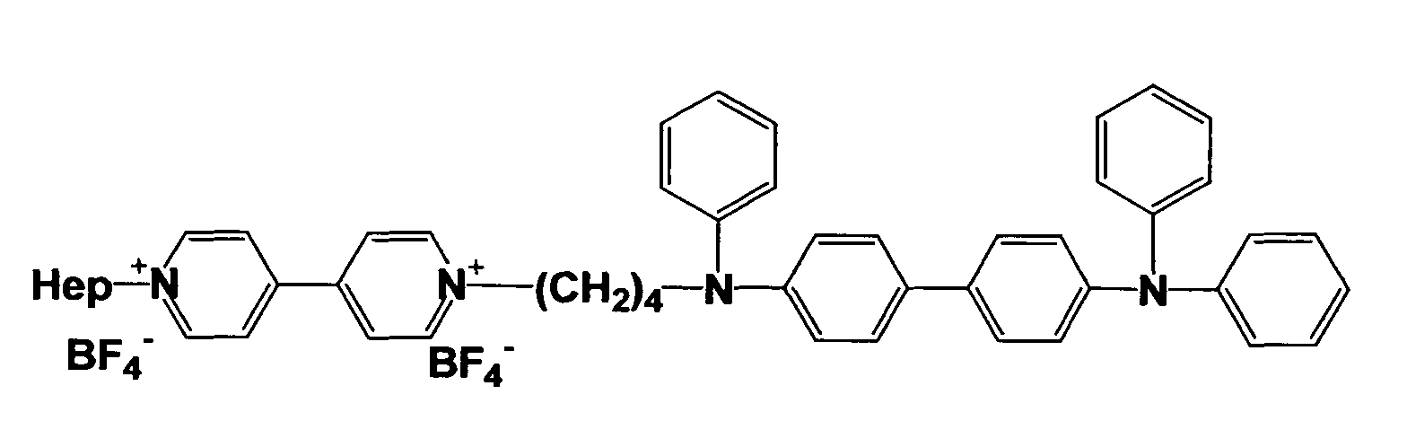

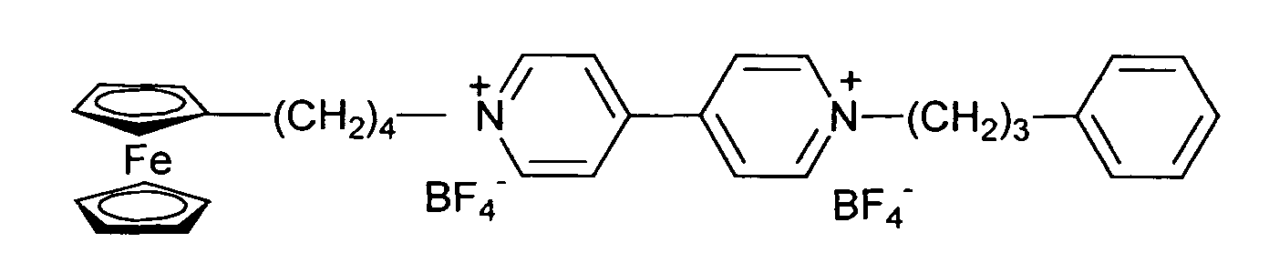
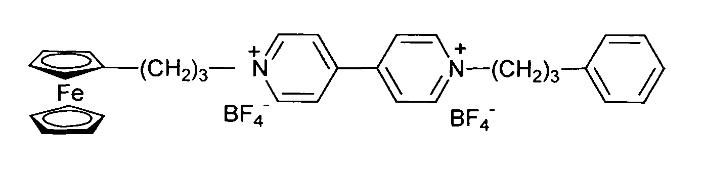


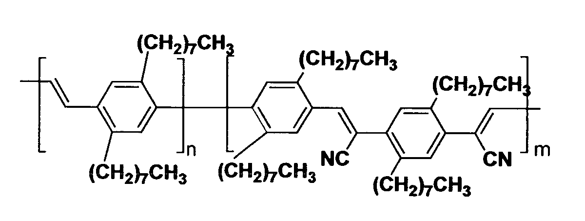
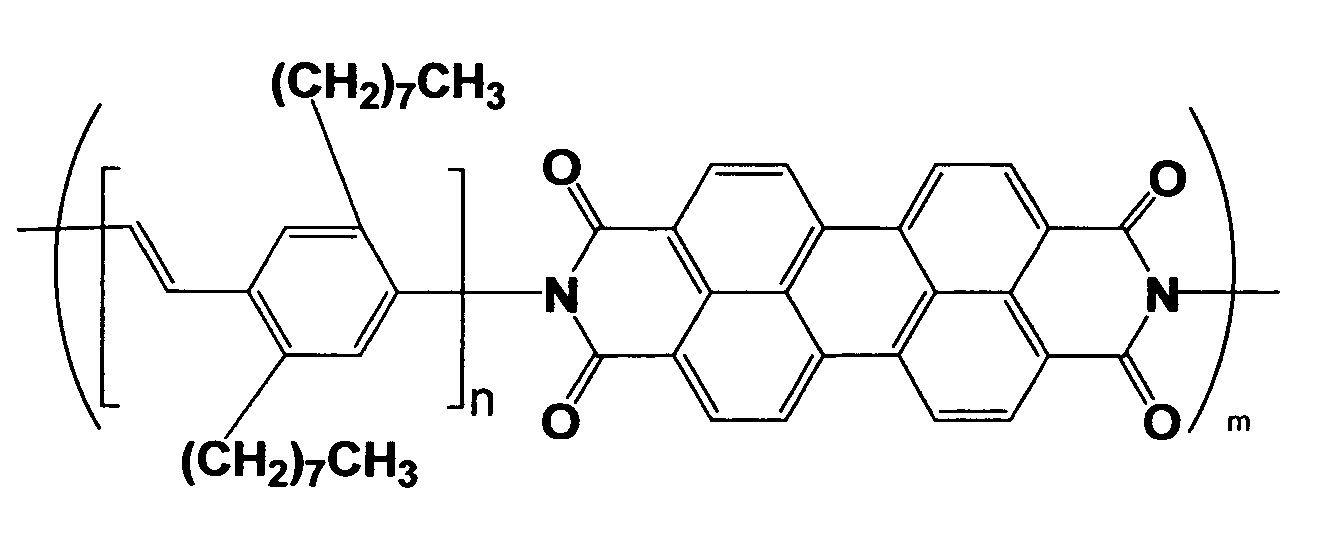
Specific examples of compounds having an
electron-accepting molecular structure include those
represented by formulas (1') to (18') below, while
specific examples of compounds having an
electron-donating molecular structure include those
represented by formulas (19') to (61'):


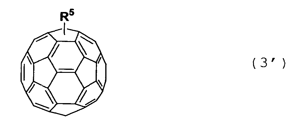
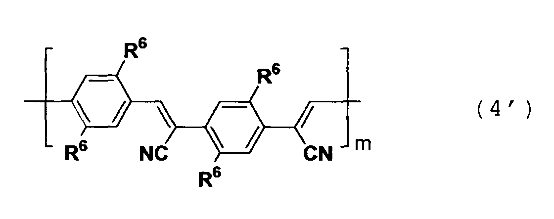


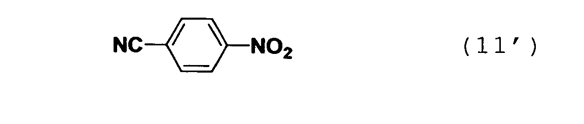

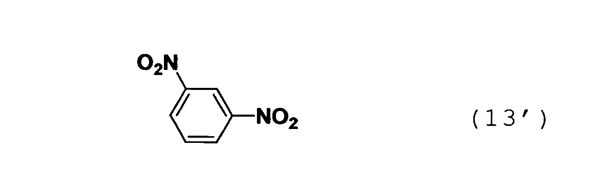

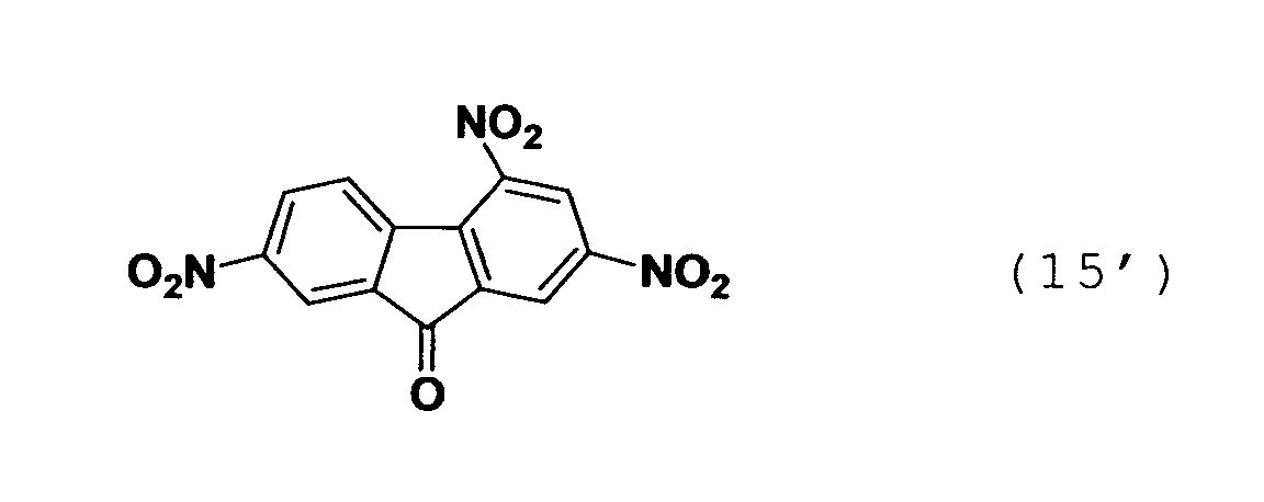


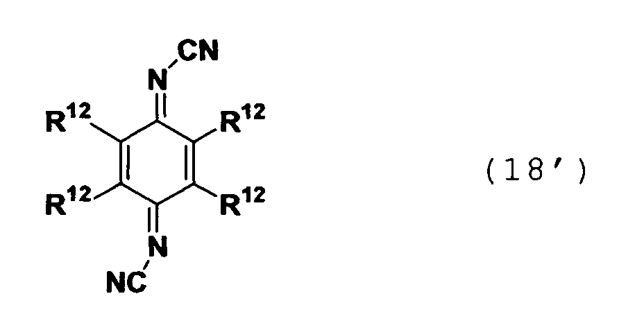
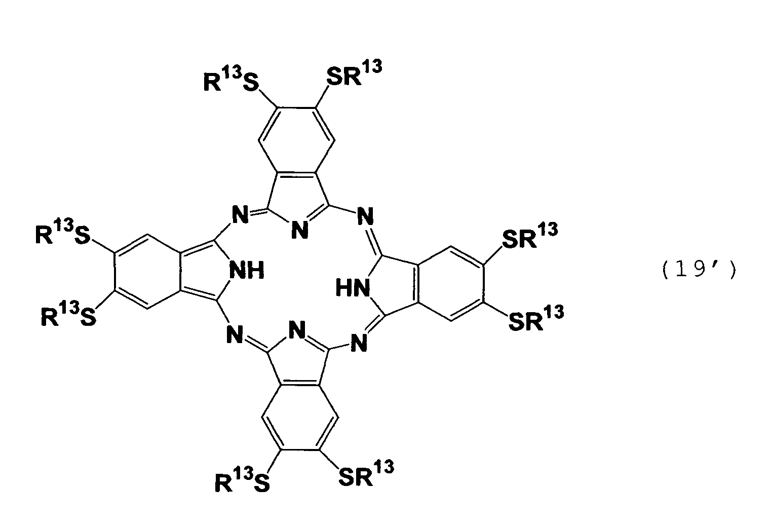

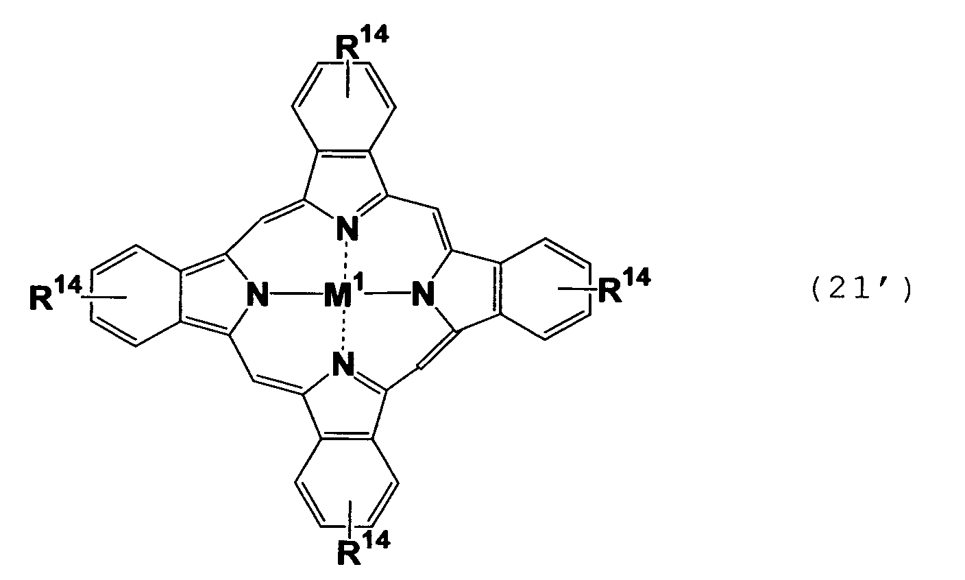
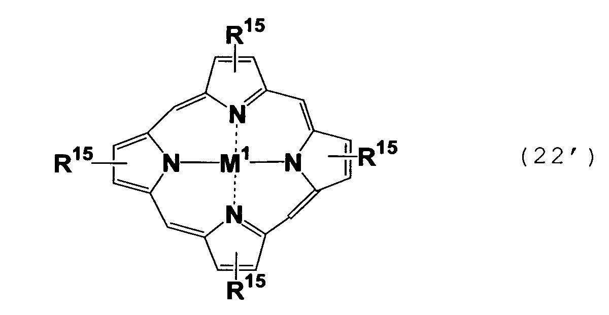
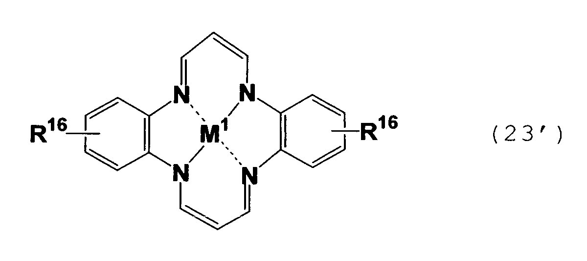
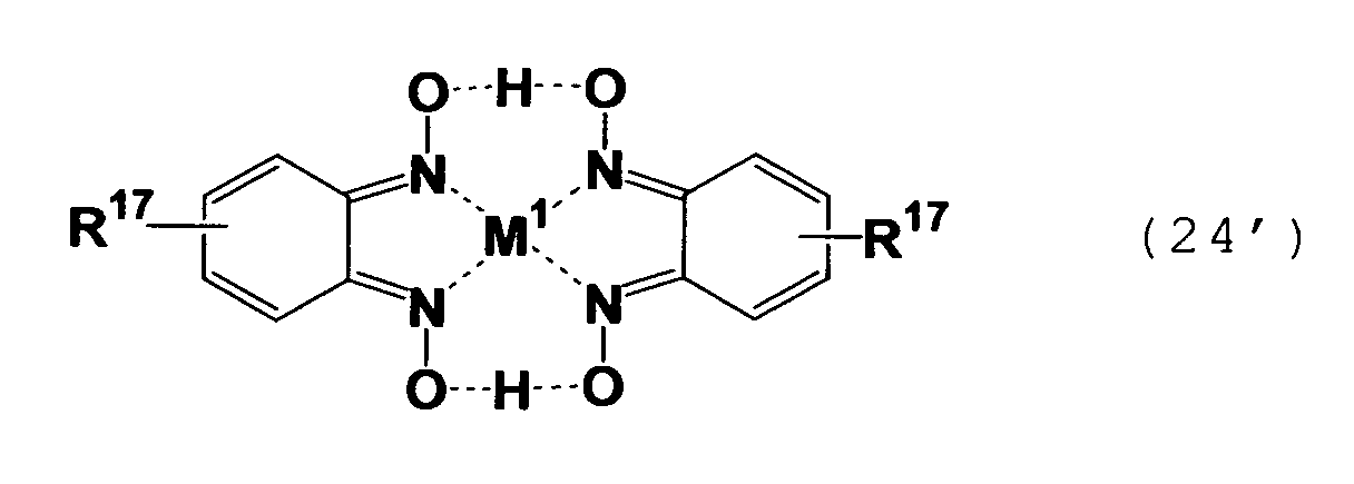
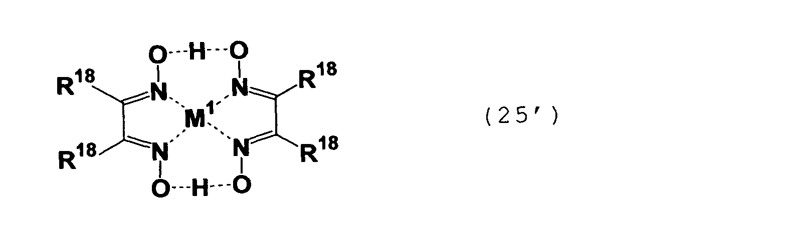
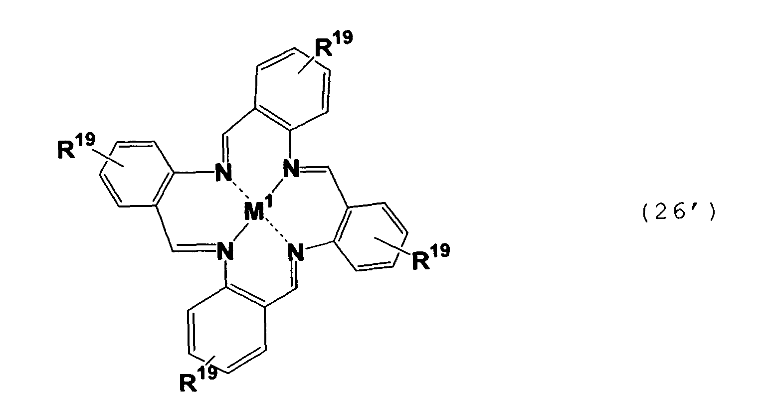

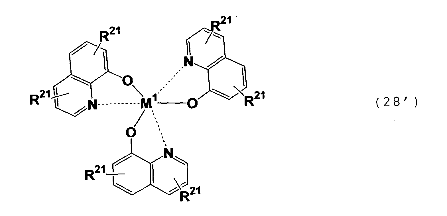


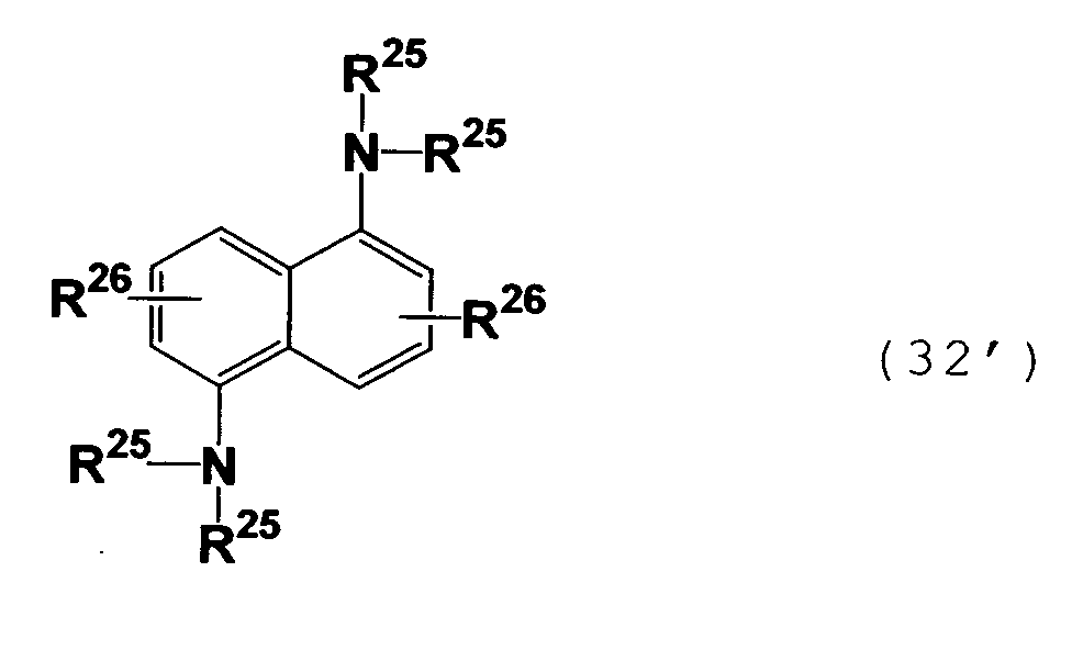

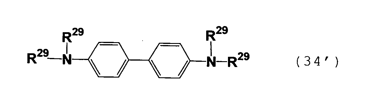
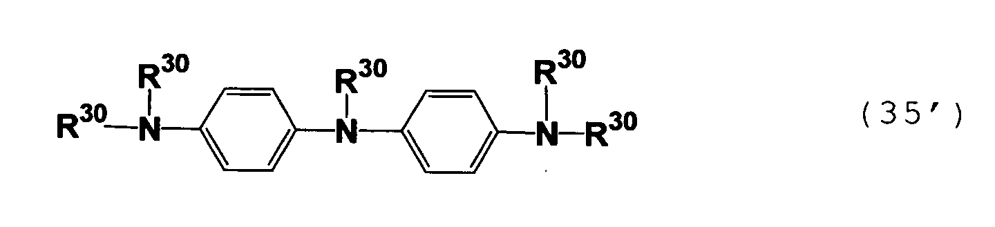
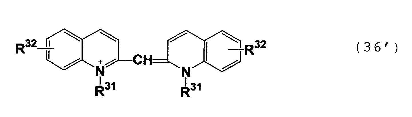

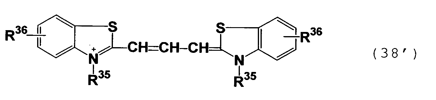

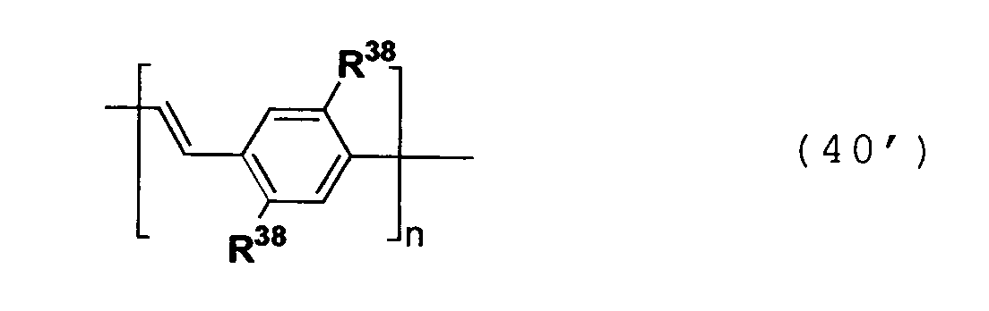


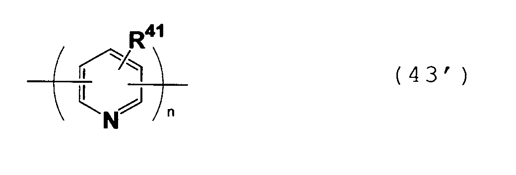

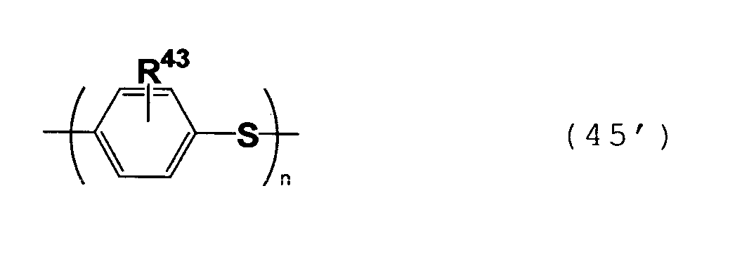


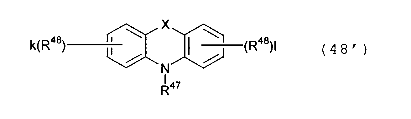


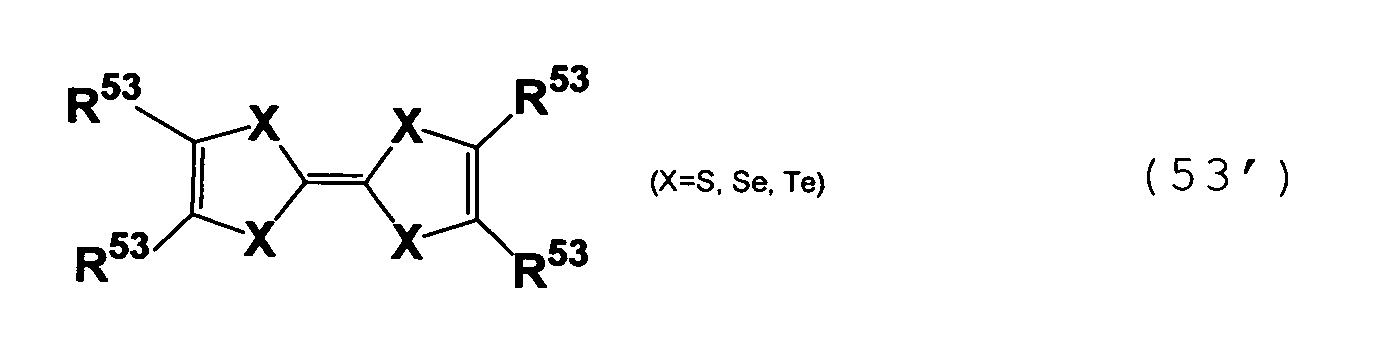


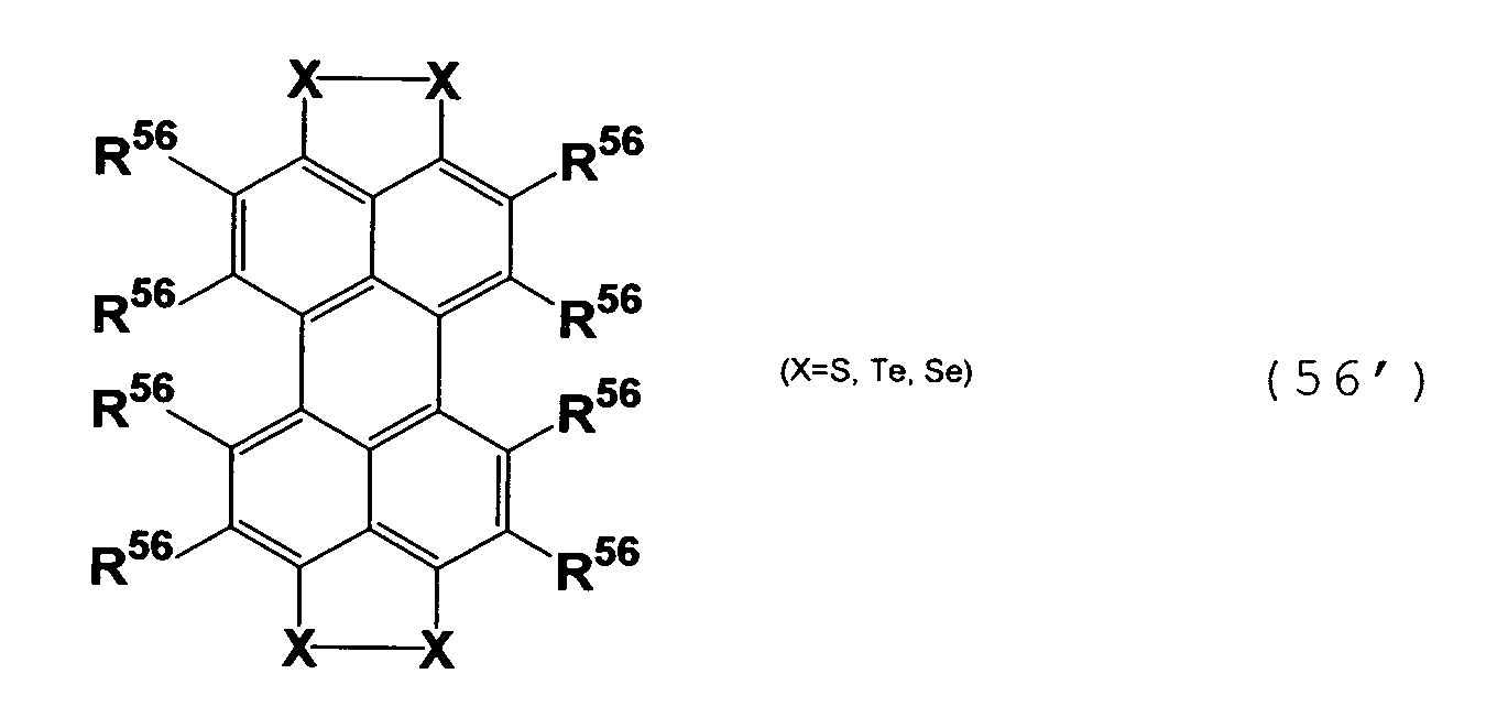

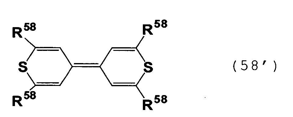

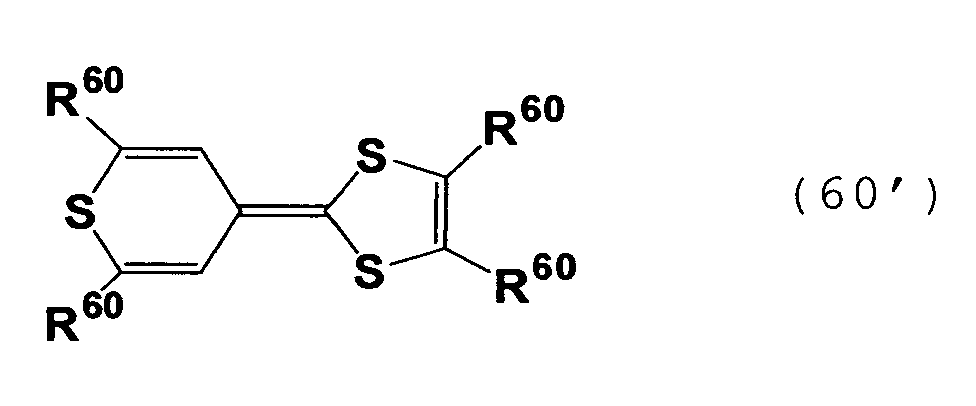
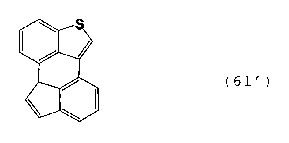
In formulas (1') to (61'), R1 to R9 and R13 to R60
may be the same or different from each other and are
each independently hydrogen; a straight-chain or
branched alkyl, alkenyl or alkoxyl group each having
1 to 10 carbon atoms; or an aryl, aralkyl, or aryloxy
group having 6 to 12 carbon atoms. R44 may be bonded
to a cyclopentadienyl ring so as to form a ring or may
form a group crosslinking cyclopentadienyl rings which
are different from each other.
R10 to R12 may be the same or different from each
other and are each independently hydrogen; halogen;
cyano, nitro, hydroxyl, amino, carboxyl, acetyl or
holmyl group; a straight-chain or branched alkyl,
alkenyl, alkoxyl, alkylthio or alkyloxycarbonyl group
having 1 to 10 carbon atoms; or an aryl, aralkyl, or
aryloxy group having 6 to 12 carbon atoms.
When a plurality of each R1 to R60 groups exist in
one of the formulas, they may be the same or different
from each other.
A- and B- may be the same or different from each
other and are each independently a counter anion
selected from the group consisting of halogen anions,
ClO4 -, BF4 -, PF6 -, CH3COO-, and CH3(C6H4)SO3 -.
In the above formulas, m and n are each
independently an integer of 1 to 1,000, preferably 2
to 500, and k and 1 indicate the number of each cyclic
hydrocarbon group which can be substituted and are each
usually an integer of 0 to 4.
M1 is a metal atom such as Cu, Zn, Co, Fe, Ti, Mg,
Ni, Mo, Os, and Ru. M2 is an alkali metal or alkaline
earth metal such as Li, Na, Mg, and Ca. M3 is Cr, Co,
Fe, Mg, Ni, Os, Ru, V, X-Hf-Y, X-Mo-Y, X-Nb-Y, X-Ti-Y,
X-V-Y or X-Zr-Y wherein X and Y are each independently
hydrogen, halogen or an alkyl group having 1 to 12 carbon
atoms and may be the same or different from each other.
Examples of the alkyl group include methyl, ethyl,
propyl, i-propyl, butyl, s-butyl, t-butyl, pentyl,
isopentyl, neopentyl, t-pentyl, hexyl, isohexyl,
heptyl, octyl, nonyl, and decyl groups. Examples of
the alkenyl group include vinyl, allyl, isopropenyl,
butylenyl, pentylenyl, and hexenyl group. Examples of
the alkoxy group include methoxy, ethoxy, propoxy,
i-propoxy, butoxy, s-butoxy, t-butoxy, pentoxy,
isopentoxy, neopentyloxy, t-pentyloxy, hexyloxy,
isohexyloxy, heptyloxy, octyloxy, nonyloxy, and
decyloxy groups. Examples of the aryl group include
phenyl, xylyl, tolyl, cumenyl, and naphthyl groups.
Examples of the aralkyl group include benzyl and
trimethyl. Examples of the aryloxy group include
phenoxy and tolyloxy groups.
Specific preferred examples of the compound
having an electron-accepting molecular structure and
the compound having an electron-donating molecular
structure include polyacetylene, polypyrrole,
polypyridine, poly-p-phenylene,
poly-p-phenylenesulfide, polyphenylenevinylene,
poly(2,5-dihexyloxy-1,4-phenylenevinylene),
poly(2,5-dioctyloxy-1,4-phenylenevinylene),
poly(2-methoxy-5-(2'-ethylhexyloxy)-1,4-phenylenevinylene),
and compounds represented by
formulas (69) to (131):


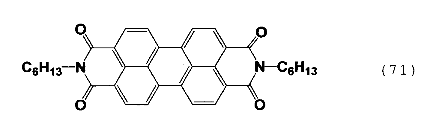
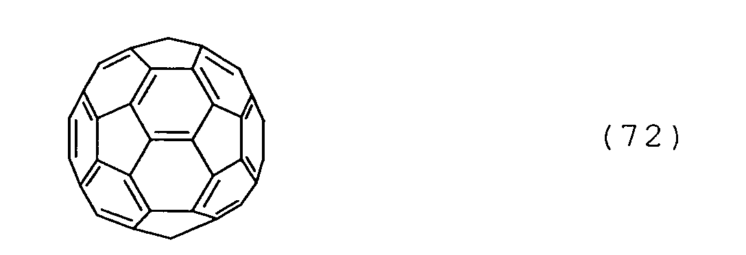

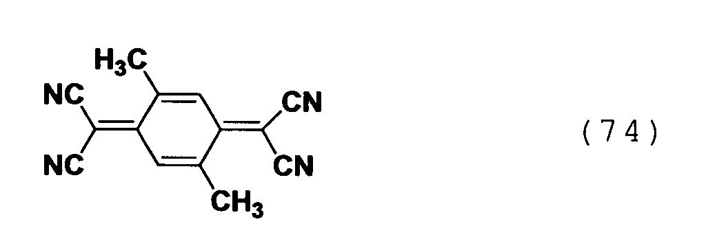


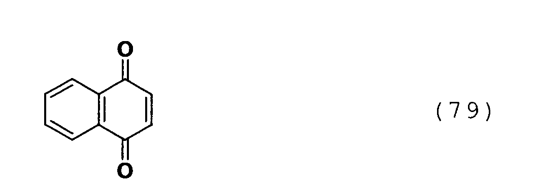
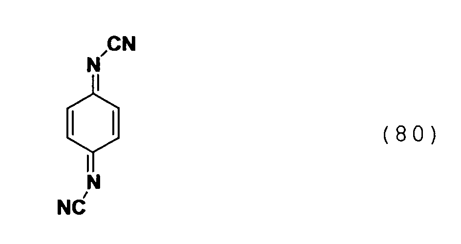


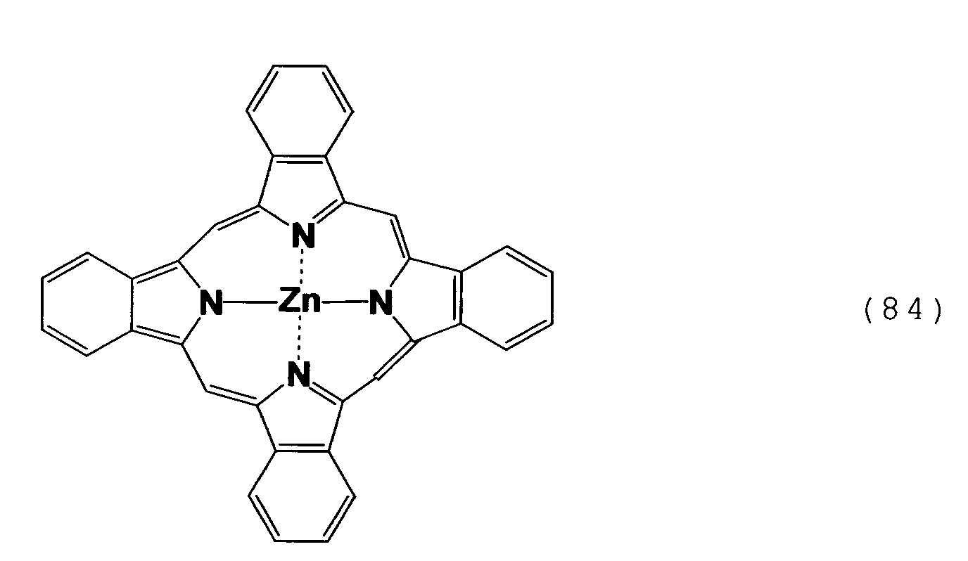


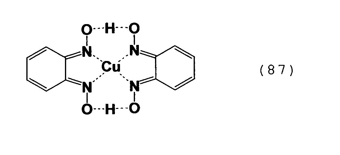
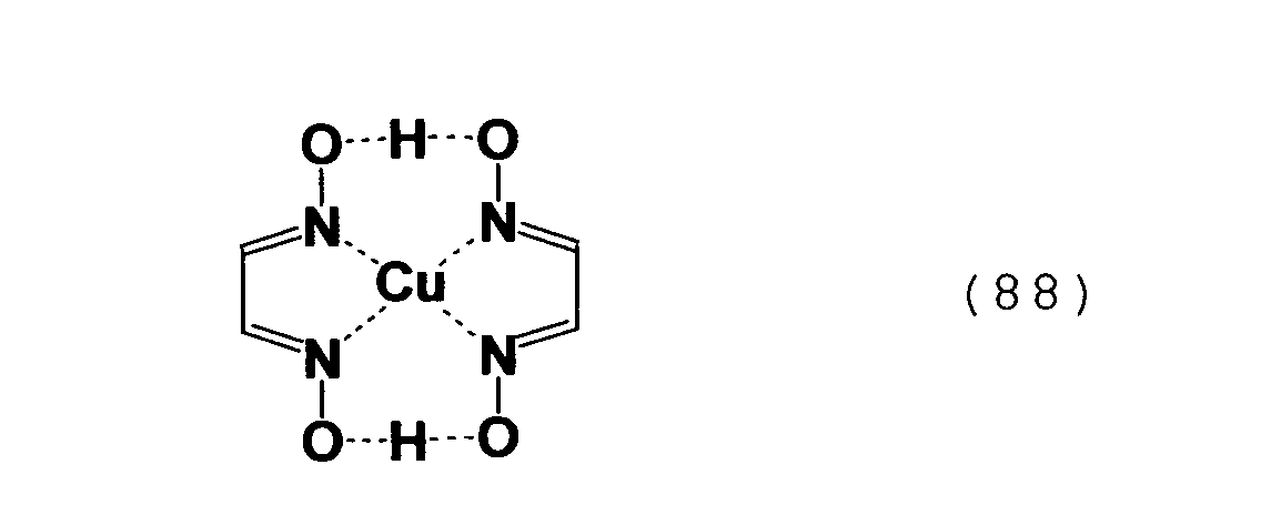
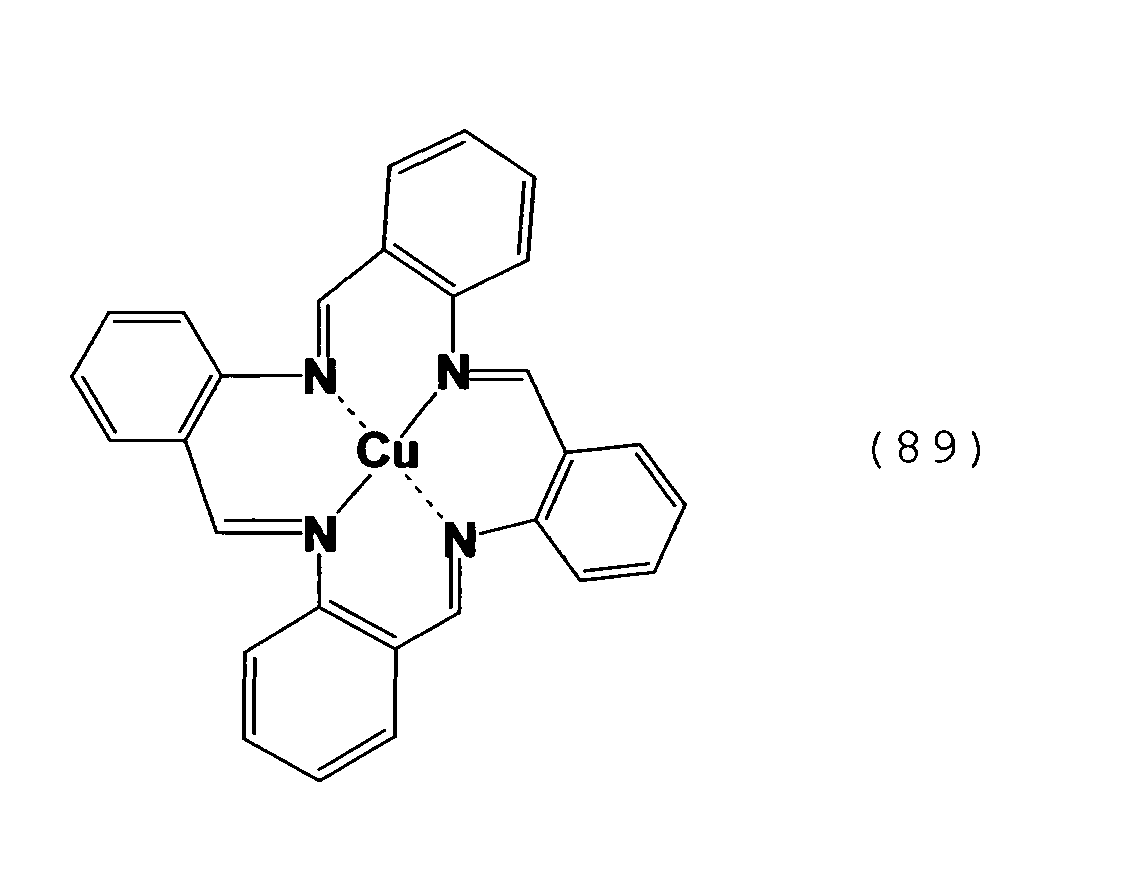
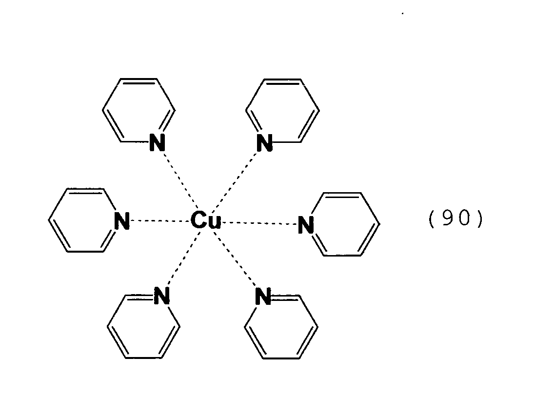
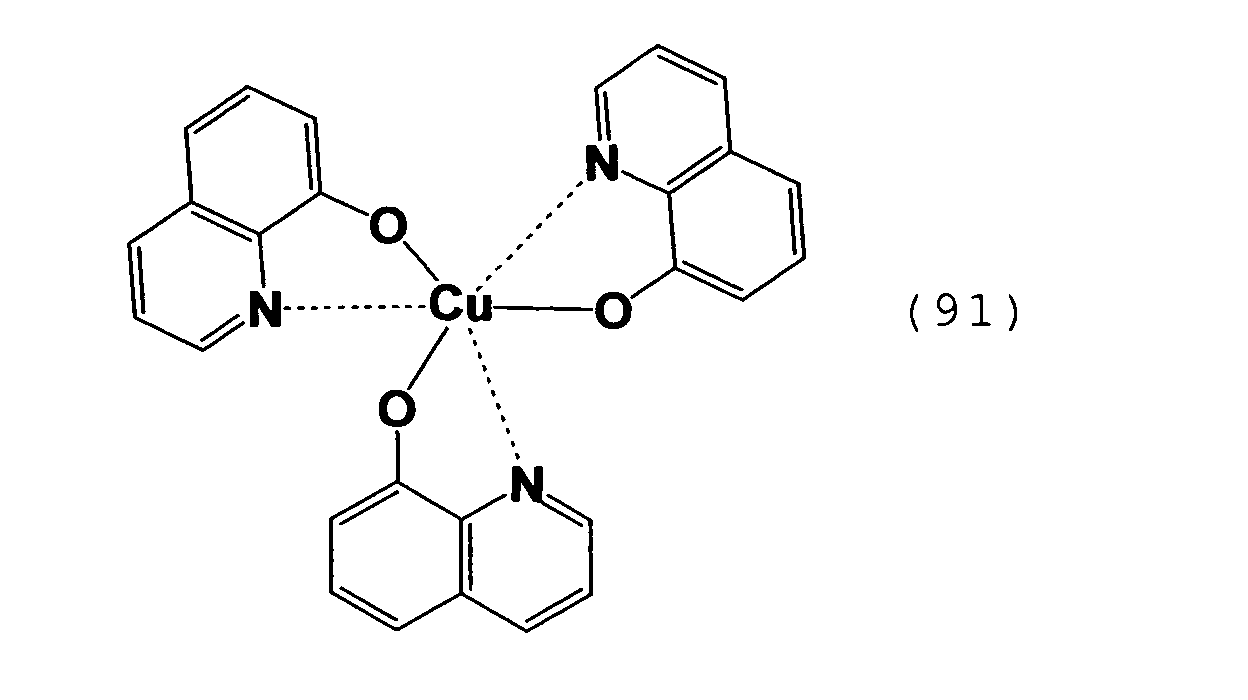
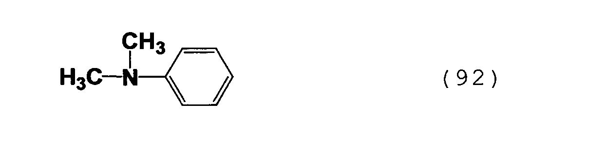


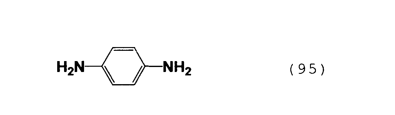

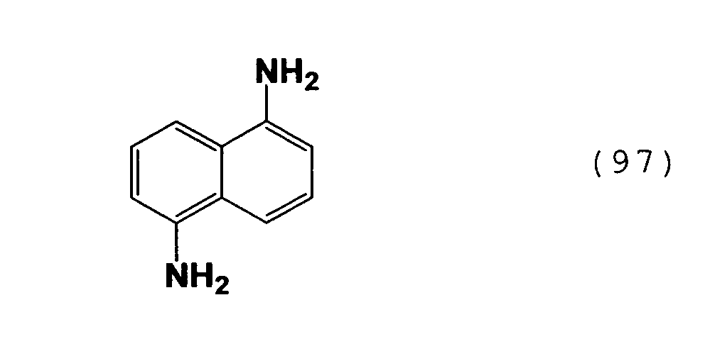
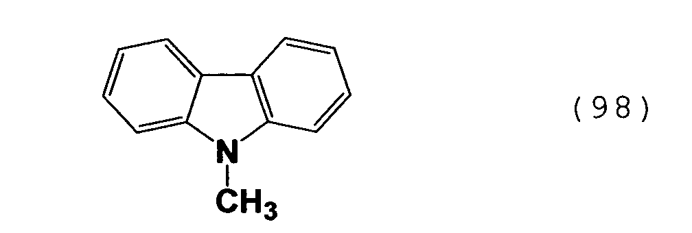


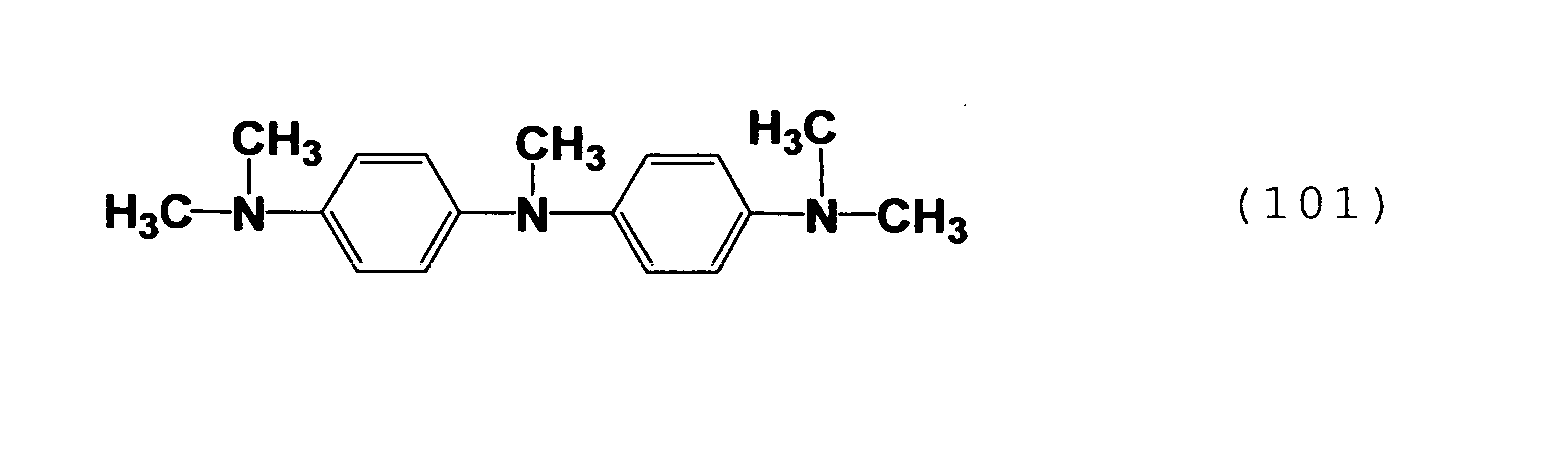


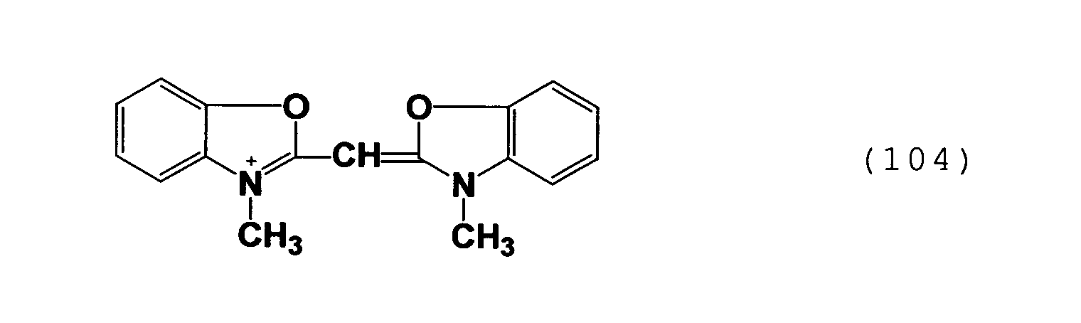

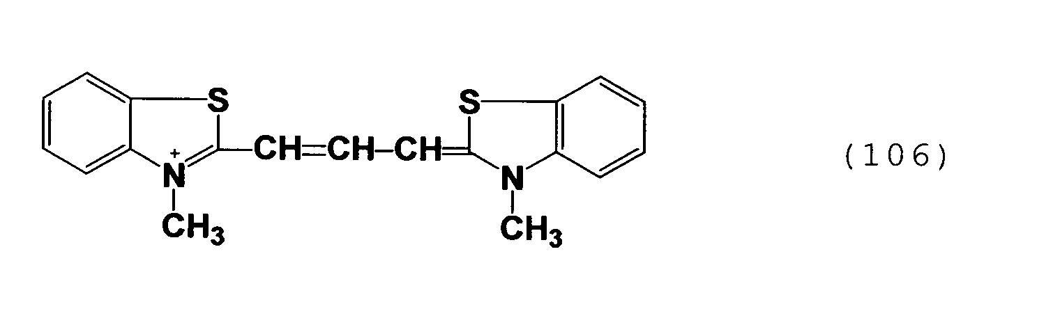
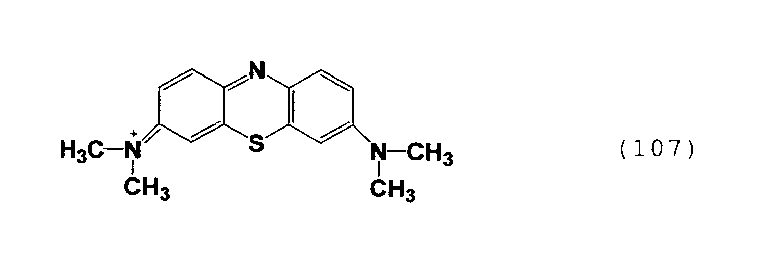
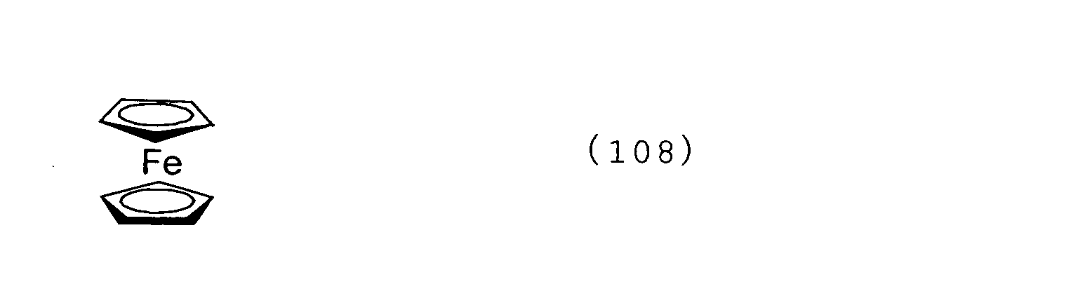


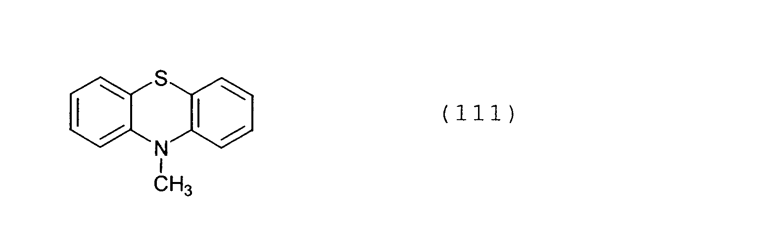





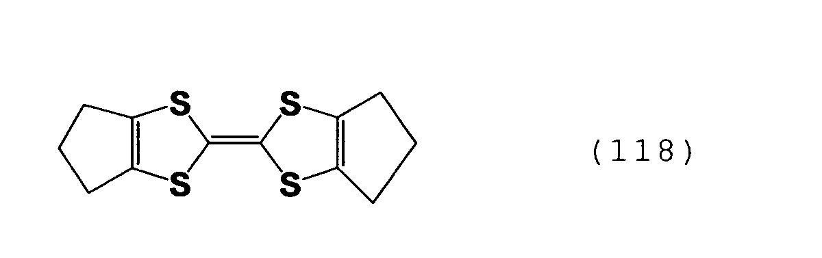

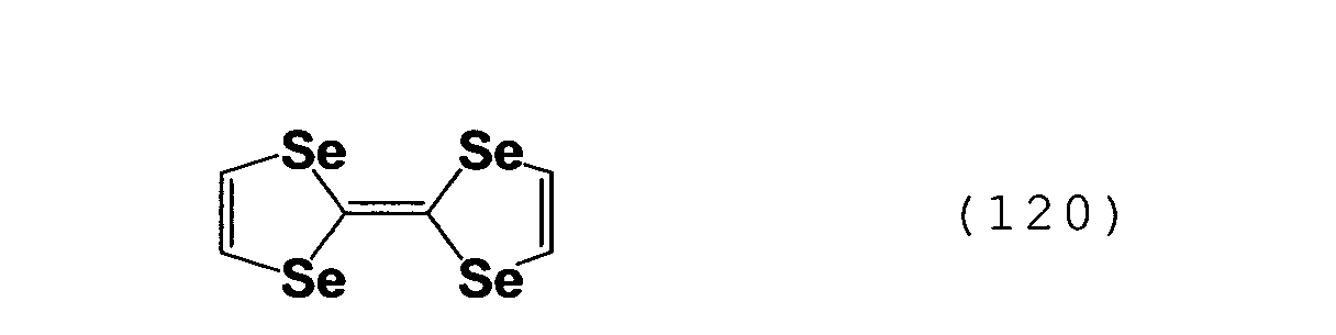
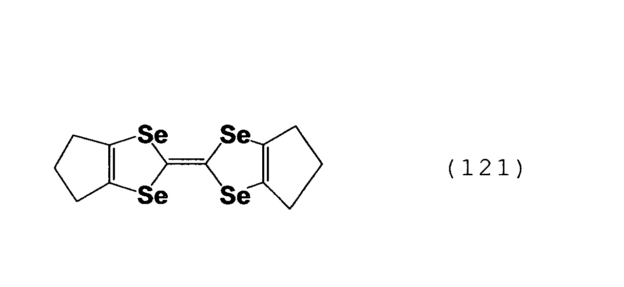


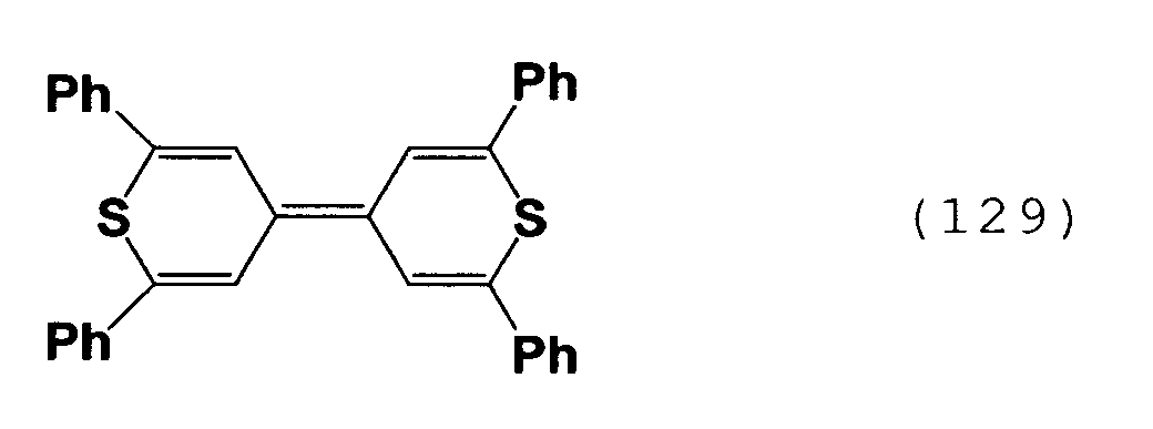
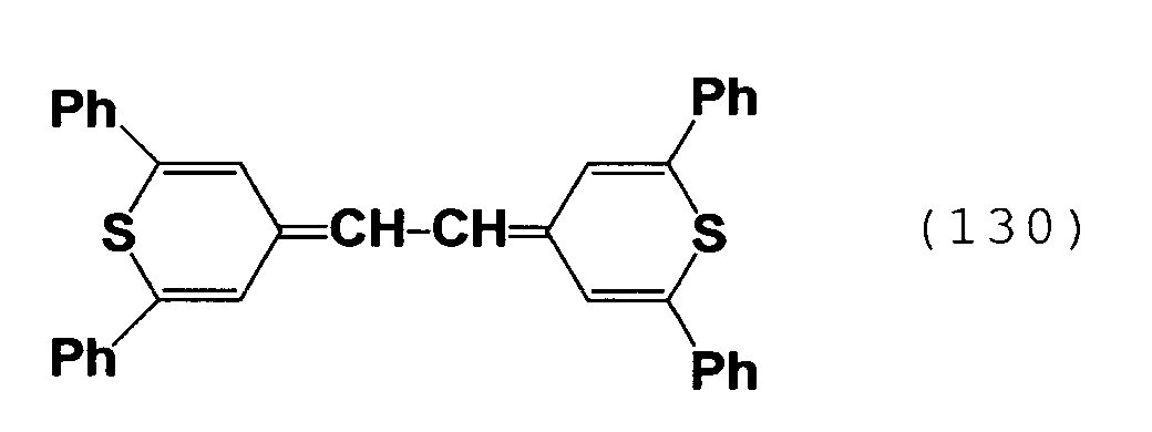

Preferred combinations of an electron-accepting
molecular structure and an electron-donating molecular
structure are a fullerene derivative (formula (3')) and
a poly(phenylenevinylene)derivative (formula (40'));
a cyano group-containing
poly(phenylenevinylene)derivative (formula (4')) and
a poly(phenylenevinylene)derivative (formula (40'));
a viologen derivative (formula (1')) and an amine
derivative (formulas (29') to (35')); a viologen
derivative (formula (1')) and a metallocene derivative
(formula (46')); a viologen derivative (formula (1'))
and a polythiophene derivative (formula (42')); a
viologen derivative (formula (1')) and a polypyrrole
derivative (formula (42')); a viologen derivative
(formula (1')) and a
poly(phenylenevinylene)derivative (formula (40')); a
perylene derivative (formula (2')) and a copper
phthalocyanine derivative (formulas (20') to (22'));
a perylene derivative (formula (2')) and a
phthalocyanine derivative (formula (19))); a perylene
derivative (formula (2')) and an amine derivative
(formulas (29') to (35')); a perylene derivative
(formula (2')) and a
poly(phenylenevinylene)derivative (formula (40')); a
perylene derivative (formula (2')) and a polythiophene
derivative (formula (42')); a perylene derivative
(formula (2')) and a polypyrrole derivative (formula
(42')); a perylene derivative (formula (2')) and a
metallocene derivative (formula (46')); a fullerene
derivative (formula (3')) and a copper phthalocyanine
derivative (formulas (20') to (22')); a fullerene
derivative (formula (3')) and an amine derivative
(formulas (29') to (35')); a fullerene derivative
(formula (3')) and a polythiophene derivative (formula
(42')); a fullerene derivative (formula (3')) and a
polypyrrole derivative (formula (42')); a fullerene
derivative (formula (3')) and a metallocene derivative
(formula (46')); a cyano group-containing
poly(phenylenevinylene)derivative (formula (4')) and
an amine derivative (formulas (29') to (35')); a cyano
group-containing poly(phenylenevinylene)derivative
(formula (4')) and a copper phthalocyanine derivative
(formulas (20') to (22')); a cyano group-containing
poly(phenylenevinylene)derivative (formula (4')) and
a polythiophene derivative (formula (42')); a cyano
group-containing poly(phenylenevinylene)derivative
(formula (4')) and a polypyrrole derivative (formula
(42')); and a cyano group-containing
poly(phenylenevinylene)derivative (formula (4')) and
a metallocene group (formula (46')).
Compounds (A) having both an electron-donating
molecular structure and an electron-accepting
molecular structure, Compounds (B) having an
electron-donating molecular structure and Compounds
(C) having an electron-accepting molecular structure
to be dispersed in the polymer forming the
photoelectric converting layer preferably have
electric conductivity. Whether or not these compounds
have electric conductivity can be easily determined in
a conventional manner. For example, whether or not
these compounds have electric conductivity can be
determined by measuring the electric conductivity in
a conventional manner after the compound are doped.
The compounds have an electric conductivity of
generally 10-6 to 106 S/cm and preferably 10-4 to 105
S/cm.
The present invention is characterized in that the
compound (A) having both an electron-donating
molecular structure and an electron-accepting
molecular structure and/or the compound (B) having an
electron-donating molecular structure and the compound
(C) having an electron-accepting molecular structure
are dispersed in the polymer forming the photoelectric
converting layer. No particular limitation is imposed
on the method of dispersing these compounds. Therefore,
the compounds may be dispersed by any method using a
homogenizer, a ball mill, a beads mill, a sand mill,
a twin roll mill, or a triple roll mill. Alternatively,
the compounds may be dispersed or dissolved using a
suitable solvent to an extent that the present
invention is not prevented from achieving the object.
Further alternatively, after a polymer precursor
and the compound (A) having both an electron-donating
molecular structure and an electron-accepting
molecular structure and/or the compound (B) having an
electron-donating molecular structure and the compound
(C) having an electron-accepting molecular structure
are dispersed, the polymer precursor may be polymerized
so as to be a polymer.
No particular limitation is imposed on an
electrically conductive substrate on which the
photoelectric converting layer is formed as long as it
can be provided with electric conductivity by a
suitable method. The electrically conductive
substrate is usually produced by laminating a
transparent electrode layer on a transparent substrate.
No particular limitation is imposed on the transparent
substrate. The material, thickness, size, and shape
of the substrate can be properly selected depending on
the purposes. For example, the substrate may be
selected from colored or colorless glasses, wire
glasses, glass blocks, and colored or colorless
transparent resins. Specific examples are polyesters
such as polyethylene terephthalate, polyamides,
polysulfones, polyethersulfones, polyether ether
ketones, polyphenylene sulfides, polycarbonates,
polyimides, polymethyl methacrylates, polystyrenes,
cellulose triacetates, and polymethyl pentenes. The
term "transparent" used herein denotes a
transmissivity of 10 to 100 percent. The substrates
used herein are those having a smooth surface at
ordinary temperature, which surface may be flat or
curved or deformed with stress.
No particular limitation is imposed on the
transparent electrode layer as long as it can achieve
the purposes of the present invention. For example,
the layer may be a metal film of gold, silver, chromium,
copper, or tungsten or an electrically conductive film
made of a metal oxide. Preferred examples of the metal
oxide include tin oxide, zinc oxide, and those obtained
by doping thereto trace amounts of components such as
Indium Tin Oxide (ITO (In2O3:Sn)), Fluorine doped Tin
Oxide (FTO (SnO2:F)), and Aluminum doped Zinc Oxide (AZO
(ZnO:Al)). The film thickness is usually from 100 to
5,000 nm and preferably from 500 to 3,000 nm. The
surface resistance (resistivity) is properly selected
depending on the use of the substrate in the present
invention, but is usually from 0.5 to 500 Ω/sq and
preferably from 2 to 50 Ω/sq.
No particular limitation is imposed on the method
of forming the transparent electrode layer. The method
is properly selected from any conventional methods
depending on the type of the above-described metal or
metal oxide used as the electrode layer. In general,
the method is selected from vacuum deposition, ion
plating, CVD, and sputtering. In any of the methods,
the transparent electrode layer is desirously formed
at a substrate temperature of 20 to 700°C.
If necessary, a semiconductor layer may be
provided between the electrically conductive substrate
and the photoelectric converting layer. Examples of
materials used for producing the semiconductor layer
include Bi2S3, CdS, CdSe, CdTe, CuInS2, CuInSe2, Fe2O3,
GaP, GaAs, InP, Nb2O5, PbS, Si, SnO2, TiO2, WO3, ZnO,
and ZnS, among which preferred are CdS, CdSe, CuInS2,
CuInSe2, Fe2O3, GaAs, InP, Nb2O5, PbS, SnO2, TiO2, WO3,
and ZnO. These materials may be used in combination.
Particularly preferred are TiO2, ZnO, SnO2, and Nb2O5,
while most preferred are TiO2 and ZnO.
The semiconductor used in the present invention
may be monocrystal or polycrystal. The crystal system
may be selected from those of anatase, rutile, or
brookite type among which preferred are those of
anatase type. The semiconductor layer may be formed
by any suitable conventional method.
The semiconductor layer may be obtained by coating
a nanoparticle dispersant or a sol solution, of the
above-mentioned semiconductor on the substrate by any
conventional method. No particular limitation is
imposed on the coating method. Therefore, the coating
may be conducted by a method wherein the semiconductor
layer is obtained in the form of film by casting;
spin-coating; dip-coating; bar-coating; and various
printing methods such as screen-printing.
The thickness of the semiconductor layer may be
properly selected but is 0.5 µm or more and 50 µm or
less and preferably 1 µm or more and 20 µm or less.
If necessary, the photoelectric converting device
of the present invention may be provided with an
electron blocking layer and/or a hole transport layer;
a hole blocking layer and/or an electron transport
layer; or a protection layer. The electron blocking
layer and/or the hole transport layer are usually
arranged between the positive pole and the
photoelectric converting layer, while the hole
blocking layer and/or the electron transport layer are
usually arranged between the negative pole and the
photoelectric converting layer. Fig. 2 shows an
example of the layer structure.
Materials for forming the electron blocking layer
and the hole transport layer may be any materials as
long as they have the function to block photogenerated
electrons or the function to transport photogenerated
holes. Specific examples of such materials include
electrically conductive polymers such as carbazole
derivatives, triazole derivatives, oxazole
derivatives, oxadiazole derivatives, imidazole
derivatives, polyarylalkane derivatives, pyrazoline
derivatives, pyrazolone derivatives, phenylenediamine
derivatives, arylamine derivatives,
amino-substituted-chalcone derivatives,
styrylanthracene derivatives, fluorenone derivatives,
hydrazone derivatives, stilbene derivatives, silazane
derivatives, aromatic tertiary amine compounds,
styrylamine compounds, aromatic dimethylidene-based
compounds, porphyrin-based compounds,
polysilane-based compounds,
poly(N-vinylcarbazole)derivatives, aniline-based
copolymers, thiophene oligomers and polythiophene.
The electron blocking layer and/or the hole
transport layer may be of a single-layered structure
composed of one or more of the materials exemplified
above or a multi-layered structure composed of a
plurality of layers each having the same or different
composition.
The electron blocking layer and/or the hole
transport layer may be formed by a method such as
vacuum-deposition, LB method, ink jet method, and a
coating method wherein any of the above-mentioned
materials is dissolved or dispersed in a solvent and
then coated by spin-coating, casting, or dip-coating.
When coating is used, a resin component may be
dissolved or dispersed with any of the above materials
thereby preparing a coating solution. Eligible resin
components are polyvinyl chloride, polycarbonate,
polystyrene, polymethylmethacrylate,
polybutylmethacrylate, polyester, polysulfone,
polyphenyleneoxide, polybutadiene,
poly(N-vinylcarbazole), hydrocarbon resins, ketone
resins, phenoxy resins, polyamide, ethyl cellulose,
polyvinyl acetate, ABS resins, polyurethane, melamine
resins, unsaturated polyester resins, alkyd resins,
epoxy resins, and silicon resins. No particular
limitation is imposed on the thickness of the electron
blocking layer and the hole transport layer. However,
the thickness is preferably from 1 nm to 5 µm, more
preferably from 5 nm to 1 µm, and particularly
preferably from 10 nm to 500 nm.
Materials for forming the hole blocking layer and
the electron transport layer may be any materials as
long as they have the function to block photogenerated
holes or the function to transport photogenerated
electrons. Specific examples of such materials
include triazole derivatives, oxazole derivatives,
oxadiazole derivatives, fluorenone derivatives,
anthraquinodimethane derivatives, anthrone
derivatives, diphenylquinone derivatives,
thiopyrandioxide derivatives, carbodiimide
derivatives, fluorenylidene methane derivatives,
distyrylpyrazine derivatives, heterocyclic
tetracarboxylic anhydrides such as
naphthaleneperylene, phthalocyanine derivatives, and
metal complexes such as those of 8-quinolinol
derivatives and those having metal phthalocyanine,
benzoxazole or benzothiazole as a ligand.
The hole blocking layer and/or the electron
transport layer may be of a single-layered structure
composed of one or more of the materials exemplified
above or a multi-layered structure composed of a
plurality of layers each having the same or different
composition.
The hole blocking layer and/or the electron
transport layer may be formed by a method such as
vacuum-deposition, LB method, ink jet method, and a
coating method wherein any of the above-mentioned
materials is dissolved or dispersed in a solvent and
then coated by spin-coating, casting, or dip-coating.
When coating is used, a resin component may be
dissolved or dispersed with any of the above materials
thereby preparing a coating solution. Eligible resin
components are the same as those exemplified with
respect to the electron blocking layer and/or the hole
transport layer. No particular limitation is imposed
on the thickness of the hole blocking layer and/or the
electron transport layer. However, the thickness is
preferably from 1 nm to 5 µm, more preferably from 5
nm to 1 µm, and particularly preferably from 10 nm to
500 nm.
The protection layer has a function to prevent
objects such as moisture and oxygen facilitating
deterioration of the device from entering thereinto.
Eligible materials for the protection layer are metals
such as In, Sn, Pb, Au, Cu, Ag, Al, Ti, and Ni; metal
oxides such as MgO, SiO, SiO2, Al2O3, GeO, NiO, CaO, BaO,
Fe2O3, Y2O3, and TiO2; metal fluorides such as MgF2, LiF,
AlF3, and CaF2; polyethylene; polypropylene,
polymethylmethacrylate; polyimide; polyurea;
polytetrafluoroethylene;
polychlorotrifluoroethylene;
polydichlorofluoroethylene; copolymers of
chlorotrifluoroethylene and
dichlorodifluoroethylene; copolymers obtained by
copolymerizing a monomer mixture containing
tetrafluoroethylene and at least one type of comonomer;
fluorine-containing copolymers having a cyclic
structure in the copolymer main chain; water-absorbing
substances with an absorptivity of 1 percent or more;
and moisture-proof substances with an absorptivity of
0.1 percent or less.
No particular limitation is imposed on the method
of forming the protective layer. Therefore, the
protective layer may be formed by any method such as
sputtering, reactive sputtering, MBE (molecular beam
epitaxy), cluster ion beam, ion plating, plasma
polymerization (high-frequency excitation ion
plating), plasma CVD, laser CVD, thermal CVD, gas
source CVD, coating, and ink jet.
The electrically conductive film formed on the
photoelectric converting layer may be formed from a
metal such as aluminum, magnesium, gold, silver,
platinum, indium, copper, and chromium, an alloy of
magnesium and silver, an electrically conductive
carbon, or a metal paste of silver, gold, or copper.
The method of forming the electrically conductive
film is properly selected from conventional methods
depending on the type of the above-exemplified
materials. Examples of conventional methods include
dry filming such as vacuum deposition, ion-plating, CVD,
and sputtering; spin-coating; dip-coating;
bar-coating; dispensing; and various printing methods
such as screen-printing.
The film thickness is usually from 100 to 5,000
µm, preferably from 500 to 3,000 µm. The surface
resistance (resistivity) is properly selected
depending on the use of the photoelectric converting
device of the present invention but is usually from 0.5
to 500 Ω/sq and preferably from 2 to 50 Ω/sq.
Alternatively, the photoelectric converting
device of the present invention may be in the form of
a laminate of a counter electrode substrate, the
photoelectric converting layer comprising the compound
(A) having both an electron donating molecular
structure and an electron accepting molecular
structure and/or the compound (B) having an electron
donating molecular structure and the compound (C)
having an electron accepting molecular structure
dispersed in the polymer, and the electrically
conductive substrate.
Examples of the counter electrode substrates
include supporting substrates having electric
conductivity per se and those obtained by forming an
electrically conductive film on supporting substrates.
No particular limitation is imposed on the
supporting substrate. The material, thickness, size,
and shape of the substrate can be properly selected
depending on the purposes. The supporting substrate
may or may not have electrical conductivity and may be
selected from metals such as gold and platinum, colored
or colorless glasses, wire glasses, glass blocks, and
colored or colorless transparent resins. Specific
examples include polyesters such as polyethylene
terephthalate, polyamides, polysulfones,
polyethersulfones, polyether ether ketones,
polyphenylene sulfides, polycarbonates, polyimides,
polymethyl methacrylates, polystyrenes, cellulose
triacetates, and polymethyl pentenes.
The substrates used herein are those having a
smooth surface at ordinary temperature, which surface
may be flat or curved or deformed with stress. The
counter electrode substrates can be obtained by forming
a film of a metal such as gold or platinum, In2O3:Sn,
SnO2:F, ZnO:Al by a conventional method such as
vacuum-deposition, electron beam vacuum deposition, or
sputtering.
When the counter electrode substrates are used,
an electrolyte layer may be provided between the
photoelectric converting layer and the counter
electrode substrate. The electrolyte layer is an ion
conductive material film containing at least one or
more substances selected from (a) polymeric matrixes,
(b) plasticizers, and (c) supporting electrolytes and
exhibits reversible oxidation-reduction properties by
(a) to (c) above or (d) redox agents.
No particular limitation is imposed on materials
usable for the polymeric matrix as long as they can be
formed in a solid or gelatinized state by itself or by
addition of a plasticizer or a supporting electrolyte
or a combination thereof. Polymeric compounds which
have been conventionally used can be used.
Examples of such polymeric compounds exhibiting
properties of the above-described polymeric matrix
include homopolymers and copolymers of
hexafluoropropylene, tetrafluoroethylene,
trifluoroethylene, ethylene, propylene, acrylonitrile,
vinylidene chloride, acrylic acid, methacrylic acid,
methyl acrylate, ethyl acrylate, methyl methacrylate,
and styrene polyfluorovinylidene. These polymers may
be used individually or in combination.
The plasticizer may be any plasticizers as long
as they are solvents which are generally used for
electrochemical cells or electric cells. Specific
examples are acetic anhydride, methanol, ethanol,
tetrahydrofuran, propylene carbonate, nitromethane,
acetonitrile, dimethylformamide, dimethylsulfoxide,
hexamethylphosphoamide, ethylene carbonate,
dimethoxyethane, γ-butyrolactone, γ-valerolactone,
sulfolane, propionnitrile, glutaronitrile,
tetrahydrofuran, adiponitrile, methoxyacetonitrile,
dimethylacetoamide, methylpyrrolidinone, dioxolane,
trimethyl phosphate, triethyl phosphate, tripropyl
phosphate, ethyldimethyl phosphate, tributyl
phosphate, tripentyl phosphate, trihexyl phosphate,
triheptyl phosphate, trioctyl phosphate, trinonyl
phosphate, tridecyl phosphate,
tris(trifluoromethyl)phosphate,
tris(pentafluoroethyl)phosphate,
triphenylpolyethylene glycol phosphate, and
polyethylene glycol. Particularly preferred examples
include propylene carbonate, ethylene carbonate,
dimethylsulfoxide, dimethoxyethane, acetonitrile, γ
-butyrolactone, sulfolane, dioxolane,
dimethylformamide, tetrahydrofuran, adiponitrile,
methoxyacetonitrile, dimethylacetoamide,
methylpyrrolidinone, trimethyl phosphate, and
triethyl phosphate. These plasticizers may be used
alone or in combination.
The supporting electrolyte may be salts, acids,
alkalis, ordinary-temperature melting salts which are
generally used in the field of electrochemistry or
electric cells.
No particular limitation is imposed on the salts.
For example, the salts may be inorganic ion salts such
as alkali metal salts and alkaline earth metal salts,
quaternary ammonium salts, cyclic quaternary ammonium
salts, and quaternary phosphonium salts.
Particularly preferred are Li salts.
Particularly preferred are Li salts.
Specific examples of the salts include Li, Na, and
K salts having a counter anion selected from halogen
ions, SCN-, ClO4 -, BF4 -, CF3SO3 -, (CF3SO2)2N-, (C2F5SO2)2N-,
PF6 -, AsF6 -, CH3COO-, CH3(C6H4)SO3 -, and (C2F5SO2)3C-.
The salts may be any of quaternary ammonium salts
having a counter anion selected from halogen ions, SCN-,
ClO4 -, BF4 -, CF3SO3 -, (CF3SO2)2N-, (C2F5SO2)2N-, PF6 -, AsF6 -,
CH3COO-, CH3(C6H4)SO3 -, and (C2F5SO2)3C-, more
specifically (CH3)4NBF4, (C2H5)4NBF4, (n-C4H9)4NBF4,
(C2H5)4NBr, (C2H5)4NClO4, (n-C4H9)4NClO4, CH3(C2H5)3NBF4,
(CH3)2(C2H5)2NBF4, (CH3)4NSO3CF3, (C2H5)4NSO3CF3,
(n-C4H9)4NSO3CF3, and those represented by the following
formulas:

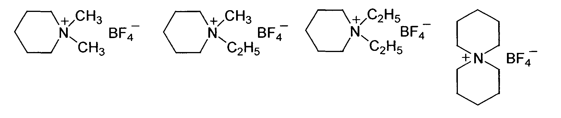

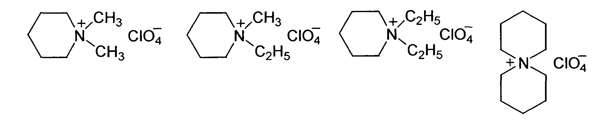 Furthermore, the salts may be any of phosphonium salts
having a counter anion selected from halogen ions, SCN-,
ClO4 -, BF4 -, CF3SO3 -, (CF3SO2)2N-, (C2F5SO2)2N-, PF6 -, AsF6 -,
CH3COO-, CH3(C6H4)SO3 -, and (C2F5SO2)3C-, more
specifically (CH3)4PBF4, (C2H5)4PBF4, (C3H7)4PBF4, and
(C4H9)4PBF4.
Furthermore, the salts may be any of phosphonium salts
having a counter anion selected from halogen ions, SCN-,
ClO4 -, BF4 -, CF3SO3 -, (CF3SO2)2N-, (C2F5SO2)2N-, PF6 -, AsF6 -,
CH3COO-, CH3(C6H4)SO3 -, and (C2F5SO2)3C-, more
specifically (CH3)4PBF4, (C2H5)4PBF4, (C3H7)4PBF4, and
(C4H9)4PBF4.
Mixtures of these salts may also be used.
No particular limitation is imposed on the acids,
which, therefore, may be inorganic acids or organic
acids. Specific examples of the acids are sulfuric
acid, hydrochloric acid, phosphoric acids, sulfonic
acids, and carboxylic acids.
No particular limitation is imposed on the alkalis
which, therefore, may be sodium hydroxide, potassium
hydroxide, and lithium hydroxide.
No particular limitation is imposed on the
ordinary-temperature melting salts. The term
"ordinary-temperature melting salt" used herein
denotes a salt comprising only ion pairs without
solvent components, in a melted state (liquid state)
at ordinary temperature, more specifically a salt
comprising ion pairs which has a melting point of 20°C
or below and will be in a liquid state at a temperature
exceeding 20°C .
The ordinary-temperature melting salt may be used
alone or in combination.
Examples of the ordinary-temperature melting salt
include those represented by the following formulas:
 wherein R is an alkyl group having 2 to 20, preferably
2 to 10 carbon atoms and X- is a counter anion selected
from halogen ions, SCN-, ClO4 -, BF4 -, (CF3SO2)2N-,
(C2F5SO2)2N-, PF6 -, AsF6 -, CH3COO-, CH3(C6H4)SO3 -, and
(C2F5SO2)3C-;
wherein R is an alkyl group having 2 to 20, preferably
2 to 10 carbon atoms and X- is a counter anion selected
from halogen ions, SCN-, ClO4 -, BF4 -, (CF3SO2)2N-,
(C2F5SO2)2N-, PF6 -, AsF6 -, CH3COO-, CH3(C6H4)SO3 -, and
(C2F5SO2)3C-;
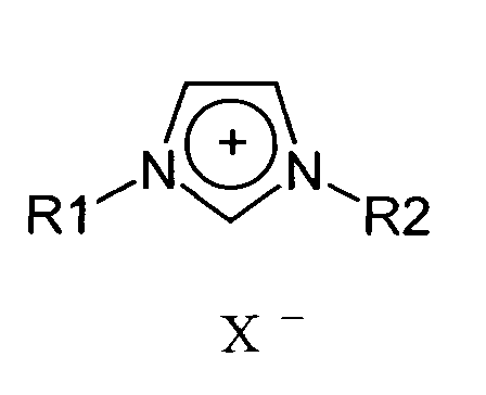 wherein R1 and R2 are each independently an alkyl group
having 1 to 10 carbon atoms, preferably methyl or ethyl
or an aralkyl group having 7 to 20, preferably 7 to 13
carbon atoms, preferably benzyl and may be the same or
different from each other and X- is a counter anion
selected from halogen ions, SCN-, ClO4 -, BF4 -,
(CF3SO2)2N-, (C2F5SO2)2N-, PF6 -, AsF6 -, CH3COO-,
CH3(C6H4)SO3 -, and (C2F5SO2)3C-; and
wherein R1 and R2 are each independently an alkyl group
having 1 to 10 carbon atoms, preferably methyl or ethyl
or an aralkyl group having 7 to 20, preferably 7 to 13
carbon atoms, preferably benzyl and may be the same or
different from each other and X- is a counter anion
selected from halogen ions, SCN-, ClO4 -, BF4 -,
(CF3SO2)2N-, (C2F5SO2)2N-, PF6 -, AsF6 -, CH3COO-,
CH3(C6H4)SO3 -, and (C2F5SO2)3C-; and
 wherein R3, R4, R5, and R6 are each independently an alkyl
group having one or more carbon atoms, preferably 1 to
6 carbon atoms, an aryl group having 6 to 12 carbon atoms
such as phenyl, or a methoxymethyl group and may be the
same or different from each other and X- is a counter
anion selected from halogen ions, SCN-, ClO4 -, BF4 -,
(CF3SO2)2N-, (C2F5SO2)2N-, PF6 -, AsF6 -, CH3COO-,
CH3(C6H4)SO3 -, and (C2F5SO2)3C-.
wherein R3, R4, R5, and R6 are each independently an alkyl
group having one or more carbon atoms, preferably 1 to
6 carbon atoms, an aryl group having 6 to 12 carbon atoms
such as phenyl, or a methoxymethyl group and may be the
same or different from each other and X- is a counter
anion selected from halogen ions, SCN-, ClO4 -, BF4 -,
(CF3SO2)2N-, (C2F5SO2)2N-, PF6 -, AsF6 -, CH3COO-,
CH3(C6H4)SO3 -, and (C2F5SO2)3C-.
No particular limitation is imposed on the amount
of the supporting electrolyte to be used. The
supporting electrolyte may be contained in the
electrolyte layer in an amount of usually 0.1 percent
by mass or more, preferably 1 percent by mass or more,
and more preferably 10 percent by mass or more and 70
percent by mass or less, preferably 60 percent by mass
or less, and more preferably 50 percent by mass or less.
The redox agents used in the present invention
will be described next.
The redox agents are those enabling a reversible
electrochemical oxidation-reduction reaction and are
not limited in type. The redox agent may be only either
one of an oxidant or a reductant or a mixture thereof
mixed at a suitable molar ratio.
Alternatively, a respective oxidation-reduction
pair of the polymeric matrix, plasticizer, or
supporting electrolyte may be added such that the
polymeric matrix, plasticizer, or supporting
electrolyte exhibits an electrochemical response.
Examples of the materials capable of making polymeric
matrix, plasticizer, or supporting electrolyte exhibit
such properties include metallocenium salts such as
ferrocenium having a counter anion selected from
halogen ions, SCN-, ClO4 -, BF4 -, CF3SO3 -, (CF3SO2)2N-,
(C2F5SO2)2N-, PF6 -, AsF6 -, CH3COO-, CH3(C6H4)SO3 -, and
(C2F5SO2)3C- and halogens such as iodine, bromine, and
chlorine.
The electrolyte layer used in the present
invention may contain another component. Examples of
the component include ultraviolet absorbing agents.
Although not restricted, typical examples of the
ultraviolet absorbing agents include organic
ultraviolet absorbing agents such as compounds having
a benzotriazole molecule structure or a benzophenone
molecule structure.
Examples of the compound having a benzotriazole
molecule structure include those represented by
formula (132) below:

In formula (132), R81 is hydrogen, halogen or an
alkyl group having 1 to 10, preferably 1 to 6 carbon
atoms. Specific examples of the halogen are fluorine,
chlorine, bromine, and iodine. Specific examples of
the alkyl group include methyl, ethyl, propyl, i-propyl,
butyl, t-butyl and cyclohexyl groups. R81 is usually
substituted at the 4- or 5-position of the
benzotriazole ring but the halogen atom and the alkyl
group are usually located at the 4-position. R82 is
hydrogen or an alkyl group having 1 to 10, preferably
1 to 6 carbon atoms. Examples of the alkyl group
include methyl, ethyl, propyl, i-propyl, butyl,
t-butyl, and cyclohexyl groups. R83 is an alkylene or
alkylidene group having 1 to 10, preferably 1 to 3 carbon
atoms. Examples of the alkylene group include
methylene, ethylene, trimethylene, and propylene
groups. Examples of the alkylidene group include
ethylidene and propylidene groups.
Specific examples of the compounds represented by
formula (132) include
3-(5-chloro-2H-benzotriazole-2-yl)-5-(1,1-dimethylethyl)-4-hydroxy-benzene propanoic acid,
3-(2H-benzotriazole-2-yl)-5-(1,1-dimethylethyl)-4-hydroxy-benzene ethanoic acid,
3-(2H-benzotriazole-2-yl)-4-hydroxybenzene ethanoic acid,
3-(5-methyl-2H-benzotriazole-2-yl)-5-(1-methylethyl )-4-hydroxybenzene propanoic acid,
2-(2'-hydroxy-5'-methylphenyl)benzotriazole,
2- [2' -hydroxy-3',5'-bis (α,α-dimethylbenzyl) phenyl] benzotriazole, 2-(2'-hydroxy-3',
5'-di-t-butylphenyl)benzotriazol,
2-(2'-hydroxy-3'-t-butyl-5'-methylphenyl)-5-chloro benzotriazole, and
3-(5-chloro-2H-benzotriazole-2-yl)-5-(1,1-dimethyl ethyl)-4-hydroxy-benzene propanoic acid octylester.
3-(5-chloro-2H-benzotriazole-2-yl)-5-(1,1-dimethylethyl)-4-hydroxy-benzene propanoic acid,
3-(2H-benzotriazole-2-yl)-5-(1,1-dimethylethyl)-4-hydroxy-benzene ethanoic acid,
3-(2H-benzotriazole-2-yl)-4-hydroxybenzene ethanoic acid,
3-(5-methyl-2H-benzotriazole-2-yl)-5-(1-methylethyl )-4-hydroxybenzene propanoic acid,
2-(2'-hydroxy-5'-methylphenyl)benzotriazole,
2- [2' -hydroxy-3',5'-bis (α,α-dimethylbenzyl) phenyl] benzotriazole, 2-(2'-hydroxy-3',
5'-di-t-butylphenyl)benzotriazol,
2-(2'-hydroxy-3'-t-butyl-5'-methylphenyl)-5-chloro benzotriazole, and
3-(5-chloro-2H-benzotriazole-2-yl)-5-(1,1-dimethyl ethyl)-4-hydroxy-benzene propanoic acid octylester.
Specific examples of the compound having a
benzophenone molecule structure include those
represented by the following formulas:


In formulas (133) to (135), R92, R93, R95, R96, R98,
and R99 may be the same or different from each other
and are each independently a hydroxyl group or an alkyl
or alkoxy group having 1 to 10, preferably 1 to 6 carbon
atoms. Examples of the alkyl group include methyl,
ethyl, propyl, i-propyl, butyl, t-butyl, and
cyclohexyl groups. Specific examples of the alkoxy
group are methoxy, ethoxy, propoxy, i-propoxy, and
butoxy groups.
R91, R94, and R97 are each independently an alkylene
or alkylidene group having 1 to 10, preferably 1 to 3
carbon atoms. Examples of the alkylene group include
methylene, ethylene, trimethylene, and propylene
groups. Examples of the alkylidene group include
ethylidene and propylidene groups.
In the above formulas, p1, p2, p3, q1, q2, and q3
are each independently an integer of 0 to 3.
Preferred examples of the compounds having a
benzophenone molecule structure, represented by
formulas (133) to (135) include
2-hydroxy-4-methoxybenzophenone-5-carboxylic acid,
2,2'-dihydroxy-4-methoxybenzophenone-5-carboxylic acid, 4-(2-hydroxybenzoyl)-3-hydroxybenzen propanoic acid, 2,4-dihydroxybenzophenone,
2-hydroxy-4-methoxybenzophenone,
2-hydroxy-4-methoxybenzophenone-5-sulfonic acid,
2-hydroxy-4-n-octoxybenzophenone,
2,2'-dihydroxy-4,4'-dimethoxybenzophenone,
2,2',4,4'-tetrahydroxybenzophenone, and
2-hydroxy-4-methoxy-2'-carboxybenzophenone.
2-hydroxy-4-methoxybenzophenone-5-carboxylic acid,
2,2'-dihydroxy-4-methoxybenzophenone-5-carboxylic acid, 4-(2-hydroxybenzoyl)-3-hydroxybenzen propanoic acid, 2,4-dihydroxybenzophenone,
2-hydroxy-4-methoxybenzophenone,
2-hydroxy-4-methoxybenzophenone-5-sulfonic acid,
2-hydroxy-4-n-octoxybenzophenone,
2,2'-dihydroxy-4,4'-dimethoxybenzophenone,
2,2',4,4'-tetrahydroxybenzophenone, and
2-hydroxy-4-methoxy-2'-carboxybenzophenone.
Needless to mention, two or more of these
ultraviolet absorbing agents may be used in
combination.
The use of the ultraviolet absorbing agent is
optional. No particular limitation is imposed on the
amount of the ultraviolet absorbing agent to be used.
However, if the agent is used, it may be contained in
the electrolyte layer in an amount of 0.1 percent by
mass or more and preferably 1 percent by mass or more,
and 20 percent by mass or less and preferably 10
percent by mass or less.
The electrolyte layer used in the present
invention may be produced as an electrolyte film. The
method of producing the electrolyte film will be
described as follows.
The electrolyte film used in the present invention
can be produced by forming a mixture obtained by
blending any of arbitrary components such as a
plasticizer, a supporting electrolyte, a redox agent,
or an ultraviolet absorbing agent in a polymeric matrix
component, into a film in a conventional manner. No
particular limitation is imposed on the forming method.
The film may be formed by extrusion, casting, or spin-
or dip-coating.
Extrusion may be conducted in a conventional
manner wherein a polymeric matrix is mixed with any of
arbitrary components such as a plasticizer, a
supporting electrolyte, a redox agent, an ultraviolet
absorbing agent and formed into a film after being
heat-melted.
Casting is conducted by mixing a polymeric matrix
with any of arbitrary components such as a plasticizer,
a supporting electrolyte, a redox agent, an ultraviolet
absorbing agent, adjusting the viscosity of the mixture
by adding a suitable diluent, and coating and drying
the diluted mixture with a conventional coater normally
used for casting thereby forming the mixture into a film.
Examples of the coater include doctor coaters, blade
coaters, rod coaters, knife coaters, reverse roll
coaters, gravure coaters, spray coaters, and curtain
coaters among which a suitable one is selected
depending on the viscosity and film thickness.
Spin coating is conducted by mixing a polymeric
matrix with any of arbitrary components such as a
plasticizer, a supporting electrolyte, a redox agent,
an ultraviolet absorbing agent, adjusting the
viscosity of the mixture by adding a suitable diluent,
and coating and drying the diluted mixture with a
commercially available spin-coater thereby forming the
mixture into a film.
Dip coating is conducted by mixing a polymeric
matrix with any of arbitrary components such as a
plasticizer, a supporting electrolyte, a redox agent,
an ultraviolet absorbing agent, adjusting the
viscosity of the mixture by adding a suitable diluent
so as to obtain a solution of the mixture, dipping and
lifting a suitable substrate therein, and drying the
solution thereby forming the mixture into a film.
The electrolyte film obtained by any of the
above-described methods exhibits an ionic conductivity
of generally 1 x 10⁻⁷ S/cm or higher, preferably 1 x
10-6 S/cm or higher, and more preferably 1 x 10⁻⁵ S/cm
or higher, at room temperature. The ionic conductivity
can be determined by a conventional method such as
complex impedance method.
No particular limitation is imposed on the
thickness of the electrolyte film. The lower limit is
usually 1 µm or more, preferably 10 µm or more, while
the upper limit is usually 3 mm or less, preferably 1
mm or less.
The photoelectric converting device of the
present invention is suppressed from the phase
separation of the photoelectric converting layer and
excellent in charge separation efficiency thereby
enhancing the light utilizing efficiency and making
possible highly efficient solar electric power
generation.
Furthermore, the photoelectric converting device
of the present invention can be relatively easily
produced and is less in burden to the environment upon
production or disposition.
The present invention will be described in more
details with reference to the following examples but
is not limited thereto.
A 5 cm square ITO glass (a transparent
electrically conductive glass obtained by forming an
Sn-doped In2O3 film on a glass substrate) with a surface
resistance of 10 Ω/sq was cleaned by alkali-washing
and plasma-ozone washing. A coating solution was
obtained by dispersing 200 mg of a compound both having
an electron-accepting molecular structure and an
electron-donating molecular structure, represented by
the formula below in a solution obtained by dissolving
500 mg of polymethylmethacrylate (manufactured by
FLUKA Ltd., Mw = about 200,000) in 10 g of chloroform.
The coating solution was spin-coated on the ITO glass
and dried sufficiently thereby obtaining a
photoelectric converting layer. The thickness of the
layer was about 4.5 µm. It was confirmed through an
observation made on the surface of the layer that the
film was uniform and clear. The photoelectric
converting layer was left standing at a temperature of
80°C for 20 hours, but no particular change was
observed.
Thereafter, aluminum was laminated at a film
forming speed of 30 Å/s and a pressure of 1.33 x 10⁻³
Pa (1 x 10⁻⁵ Torr) over the photoelectric converting
layer so as to be about 100 nm in thickness thereby
obtaining a photoelectric converting device.
A light of a 100 W tungsten lump, uniformed through
a diffuser was illuminated from the glass substrate
side to the device, and the electric current thereof
when the device was short-circuited was measured
thereby confirming that a current of 4 µA was obtained
and the device exhibited excellent photoelectric
converting properties.
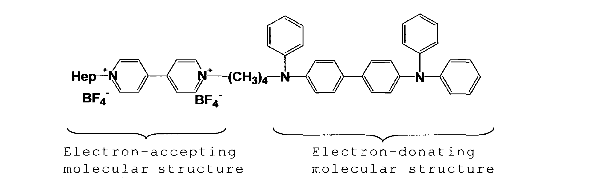
A 5 cm square ITO glass (a transparent
electrically conductive glass obtained by forming an
Sn-doped In2O3 film on a glass substrate) with a surface
resistance of 10 Ω/sq was cleaned by alkali-washing
and plasma-ozone washing. A coating solution was
obtained by dispersing 200 mg of fullerene (C60) as a
compound having an electron-accepting molecular
structure and 100 mg of Compound (a)
(poly(2,5-dihexyloxy-1,4-phenylenevinylene)
manufactured by ALDRICH Ltd.) indicated below as a
compound having an electron-donating molecular
structure in a solution obtained by dissolving 500 mg
of polymetylmethacrylate (manufactured by FLUKA Ltd.,
Mw = about 200,000) in 10 g of chloroform. The coating
solution was spin-coated on the ITO glass and dried
sufficiently thereby obtaining a photoelectric
converting layer. The thickness of the layer was about
5 µm. It was confirmed through an observation made on
the surface of the layer that the film was uniform and
clear. The photoelectric converting layer was left
standing at a temperature of 80°C for 20 hours, but no
particular change was observed.
Thereafter, aluminum was laminated at a film
forming speed of 30 Å/s and a pressure of 1.33 x 10⁻³
Pa (1 x 10⁻⁵ Torr) over the photoelectric converting
layer so as to be about 100 nm in thickness thereby
obtaining a photoelectric converting device.
A light of a 100 W tungsten lump, uniformed through
a diffuser was illuminated from the glass substrate
side to the device, and the electric current thereof
when the device was short-circuited was measured
thereby confirming that a current of 2.1 µA was
obtained and the device exhibited excellent
photoelectric converting properties.

Poly[(3,4-ethylenedioxy)-2,5-thiophene]·
polystyrene sulfonate dispersant (manufactured by
Bayer Ltd under the name of "Baytron P", solid content :
1.3 %) was spin-coated on a 5 cm square ITO glass (a
transparent electrically conductive glass obtained by
forming an Sn-doped In2O3 film on a glass substrate)
with a surface resistance of 10 Ω/sq having been
cleaned by alkali-washing and plasma-ozone washing and
vacuum-dried at a temperature of 150°C for 2 hours
thereby forming a coating layer with a thickness of 100
nm. On the coated layer was spin-coated a coating
solution obtained by dispersing 200 mg of C60 as a
compound having an electron-accepting molecular
structure and 100 mg of Compound (a) used in Example
2 as a compound having an electron-donating molecular
structure in a solution obtained by dissolving 500 mg
of polymetylmethacrylate (manufactured by FLUKA Ltd.,
Mw = about 200, 000) in 10 g of chloroform. The coating
solution was dried sufficiently thereby obtaining a
photoelectric converting layer. The thickness of the
layer was about 5 µm. It was confirmed through an
observation made on the surface of the layer that the
film was uniform and clear. The photoelectric
converting layer was left standing at a temperature of
80°C for 20 hours, but no particular change was
observed.
Thereafter, aluminum was laminated at a film
forming speed of 30 Å/s and a pressure of 1.33 x 10⁻³
Pa (1 x 10⁻⁵ Torr) over the photoelectric converting
layer so as to be about 100 nm in thickness thereby
obtaining a photoelectric converting device.
A light of a 100 W tungsten lump, uniformed through
a diffuser was illuminated from the glass substrate
side to the device, and the electric current thereof
when the device was short-circuited was measured
thereby confirming that a current of 3.5 µA was
obtained and the device exhibited excellent
photoelectric converting properties.
Poly[(3,4-ethylenedioxy)-2,5-thiophene]·
polystyrene sulfonate dispersant (manufactured by
Bayer Ltd under the name of "Baytron P", solid content :
1.3 %) was spin-coated on a 5 cm square ITO glass (a
transparent electrically conductive glass obtained by
forming an Sn-doped In2O3 film on a glass substrate)
with a surface resistance of 10 Ω/sq having been
cleaned by alkali-washing and plasma-ozone washing and
vacuum-dried at a temperature of 150°C for 2 hours
thereby forming a coating layer with a thickness of 100
nm. On the coated layer was spin-coated a coating
solution obtained by dispersing 200 mg of Compound (b)
having both an electron-accepting molecular structure
and an electron-donating molecular structure,
represented by the formula given below in a solution
obtained by dissolving 500 mg of
(poly(2,5-dihexyloxy-1,4-phenylenevinylene)
manufactured by ALDRICH Ltd.) in 10 g of chloroform.
The coating solution was dried sufficiently thereby
obtaining a photoelectric converting layer. The
thickness of the layer was about 5 µm. It was
confirmed through an observation made on the surface
of the layer that the film was uniform and clear. The
photoelectric converting layer was left standing at a
temperature of 80°C for 20 hours, but no particular
change was observed.
Thereafter, aluminum was laminated at a film
forming speed of 30 Å/s and a pressure of 1.33 x 10⁻³
Pa (1 x 10⁻⁵ Torr) over the photoelectric converting
layer so as to be about 100 nm in thickness thereby
obtaining a photoelectric converting device.
A light of a 100 W tungsten lump, uniformed through
a diffuser was illuminated from the glass substrate
side to the device, and the electric current thereof
when the device was short-circuited was measured
thereby confirming that a current of 4.2 µA was
obtained and the device exhibited excellent
photoelectric converting properties.

Poly[(3,4-ethylenedioxy)-2,5-thiophene]·
polystyrene sulfonate dispersant (manufactured by
Bayer Ltd under the name of "Baytron P", solid content :
1.3 %) was spin-coated on a 5 cm square ITO glass (a
transparent electrically conductive glass obtained by
forming an Sn-doped In2O3 film on a glass substrate)
with a surface resistance of 10 Ω/sq having been
cleaned by alkali-washing and plasma-ozone washing and
vacuum-dried at a temperature of 150°C for 2 hours
thereby forming a coating layer with a thickness of 100
nm. On the coated layer was spin-coated a coating
solution obtained by dispersing 200 mg of Compound (c)
having an electron-accepting molecular structure
represented by the formula given below and 100 mg of
Compound (d) having an electron-donating molecular
structure, represented by the formula given below in
a solution obtained by dissolving 500 mg of
(poly(2,5-dihexyloxy-1,4-phenylenevinylene)
manufactured by ALDRICH Ltd.) in 10 g of chloroform.
The coating solution was dried sufficiently thereby
obtaining a photoelectric converting layer. The
thickness of the layer was about 5 µm. It was
confirmed through an observation made on the surface
of the layer that the film was uniform and clear. The
photoelectric converting layer was left standing at a
temperature of 80°C for 20 hours, but no particular
change was observed.
Thereafter, aluminum was laminated at a film
forming speed of 30 Å/s and a pressure of 1.33 x 10⁻³
Pa (1 x 10⁻⁵ Torr) over the photoelectric converting
layer so as to be about 100 nm in thickness thereby
obtaining a photoelectric converting device.
A light of a 100 W tungsten lump, uniformed through
a diffuser was illuminated from the glass substrate
side to the device, and the electric current thereof
when the device was short-circuited was measured
thereby confirming that a current of 4.5 µA was
obtained and the device exhibited excellent
photoelectric converting properties.

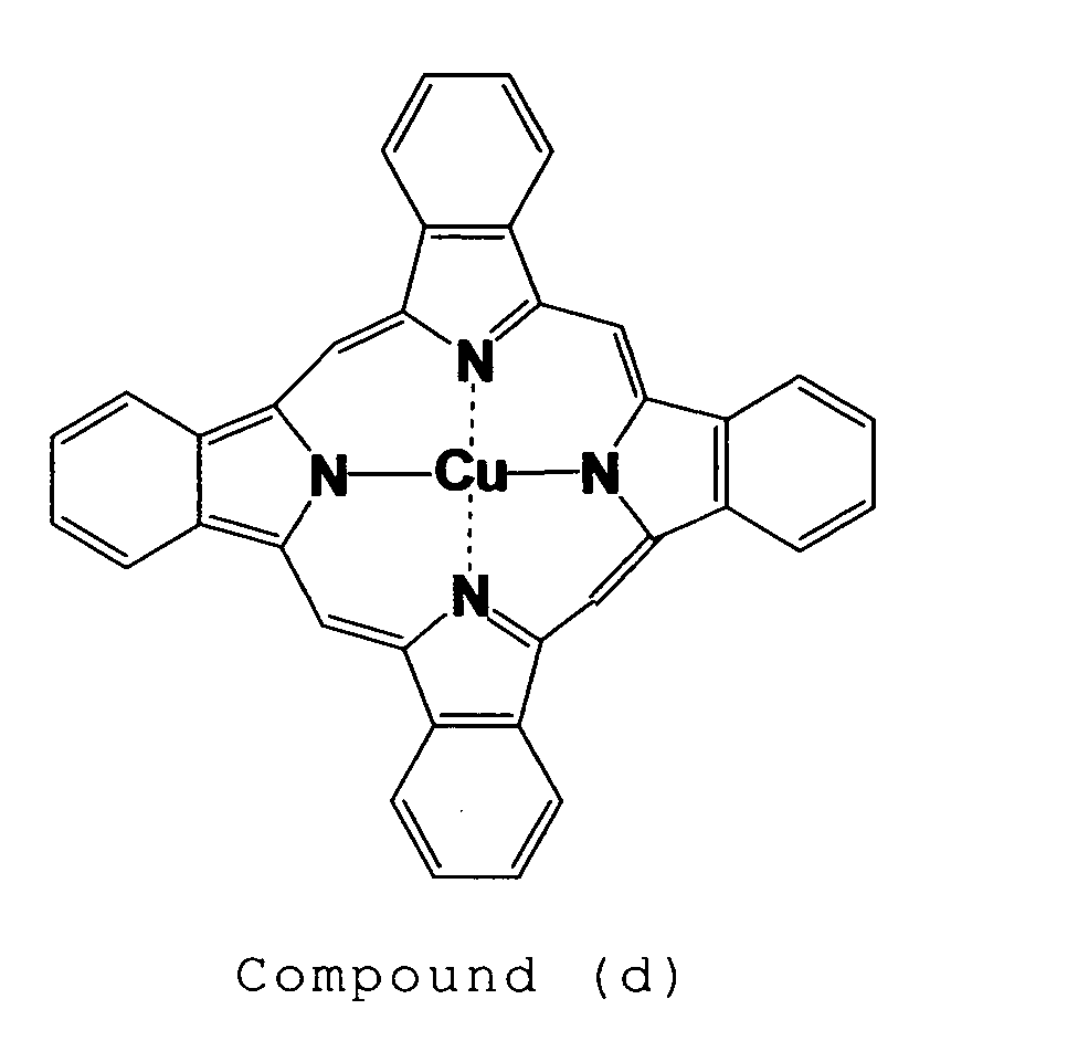
Claims (4)
- A photoelectric converting device which has a photoelectric converting layer comprising an organic compound (A) having both an electron donating molecular structure and an electron accepting molecular structure dispersed in a polymer.
- A photoelectric converting device which has a photoelectric converting layer comprising an organic compound (B) having an electron donating molecular structure and an organic compound (C) having an electron accepting molecular structure, dispersed in a polymer.
- The photoelectric converting device according to claim 1 wherein said polymer is an electrically conductive polymeric compound.
- The photoelectric converting device according to claim 2 wherein said polymer is an electrically conductive polymeric compound.
Applications Claiming Priority (5)
| Application Number | Priority Date | Filing Date | Title |
|---|---|---|---|
| JP2002346304 | 2002-11-28 | ||
| JP2002346304 | 2002-11-28 | ||
| JP2002367286 | 2002-12-18 | ||
| JP2002367286 | 2002-12-18 | ||
| PCT/JP2003/012963 WO2004049458A1 (en) | 2002-11-28 | 2003-10-09 | Photoelectric conversion element |
Publications (2)
| Publication Number | Publication Date |
|---|---|
| EP1566845A1 true EP1566845A1 (en) | 2005-08-24 |
| EP1566845A4 EP1566845A4 (en) | 2009-08-12 |
Family
ID=32396300
Family Applications (1)
| Application Number | Title | Priority Date | Filing Date |
|---|---|---|---|
| EP03751417A Withdrawn EP1566845A4 (en) | 2002-11-28 | 2003-10-09 | PHOTOELECTRIC CONVERSION ELEMENT |
Country Status (5)
| Country | Link |
|---|---|
| US (1) | US20050263183A1 (en) |
| EP (1) | EP1566845A4 (en) |
| JP (2) | JPWO2004049458A1 (en) |
| AU (1) | AU2003271146A1 (en) |
| WO (1) | WO2004049458A1 (en) |
Cited By (2)
| Publication number | Priority date | Publication date | Assignee | Title |
|---|---|---|---|---|
| WO2008018931A3 (en) * | 2006-06-13 | 2008-04-03 | Plextronics Inc | Organic photovoltaic devices comprising fullerenes and derivatives thereof |
| US8715606B2 (en) | 2007-12-21 | 2014-05-06 | Plextronics, Inc. | Organic photovoltaic devices comprising fullerenes and derivatives thereof and improved methods of making fullerene derivatives |
Families Citing this family (40)
| Publication number | Priority date | Publication date | Assignee | Title |
|---|---|---|---|---|
| WO2004049458A1 (en) * | 2002-11-28 | 2004-06-10 | Nippon Oil Corporation | Photoelectric conversion element |
| US20050150544A1 (en) * | 2003-12-05 | 2005-07-14 | Sharp Kabushiki Kaisha | Dye-sensitized solar cell |
| US7326955B2 (en) * | 2004-08-05 | 2008-02-05 | The Trustees Of Princeton University | Stacked organic photosensitive devices |
| US7196366B2 (en) * | 2004-08-05 | 2007-03-27 | The Trustees Of Princeton University | Stacked organic photosensitive devices |
| DE102005010978A1 (en) | 2005-03-04 | 2006-09-07 | Technische Universität Dresden | Photoactive component with organic layers |
| JP5023455B2 (en) * | 2005-03-28 | 2012-09-12 | 大日本印刷株式会社 | Organic thin film solar cell manufacturing method and organic thin film solar cell |
| JP4758684B2 (en) * | 2005-06-14 | 2011-08-31 | セイコーエプソン株式会社 | Photoelectric conversion element and electronic device |
| JP2007081137A (en) * | 2005-09-14 | 2007-03-29 | Fujifilm Corp | Photoelectric conversion device and solid-state imaging device |
| JP4857799B2 (en) | 2006-02-10 | 2012-01-18 | セイコーエプソン株式会社 | Photoelectric conversion element, method for manufacturing photoelectric conversion element, and electronic device |
| JP5369366B2 (en) * | 2006-02-16 | 2013-12-18 | ソニー株式会社 | Photoelectric conversion element, semiconductor device and electronic device |
| EP1999804A2 (en) * | 2006-03-20 | 2008-12-10 | General Electric Company | Opto-electronic devices exhibiting enhanced efficiency |
| WO2007121252A2 (en) * | 2006-04-11 | 2007-10-25 | Konarka Technologies, Inc. | Tandem photovoltaic cells |
| KR101165656B1 (en) * | 2006-05-02 | 2012-07-16 | 미쓰비시 가가꾸 가부시키가이샤 | Method for manufacturing organic photoelectric conversion element and organic photoelectric conversion element |
| ATE528803T1 (en) * | 2006-08-07 | 2011-10-15 | Univ Wake Forest | PRODUCTION OF ORGANIC COMPOSITE MATERIALS |
| JP2012019235A (en) * | 2006-08-14 | 2012-01-26 | Fujifilm Corp | Solid-state imaging device |
| JP2008072090A (en) * | 2006-08-14 | 2008-03-27 | Fujifilm Corp | Photoelectric conversion device and solid-state imaging device |
| JP5164018B2 (en) * | 2006-08-31 | 2013-03-13 | 株式会社豊田中央研究所 | Light energy conversion material |
| DE102006046210B4 (en) * | 2006-09-29 | 2013-03-28 | Siemens Aktiengesellschaft | Process for the preparation of an organic photodetector |
| DE102006059369A1 (en) * | 2006-12-15 | 2008-06-26 | Industrial Technology Research Institute, Chutung | photocell |
| US20090065053A1 (en) * | 2007-08-24 | 2009-03-12 | Julian Gulbinski | Photovoltaic device |
| JP4852497B2 (en) * | 2007-08-27 | 2012-01-11 | 富士フイルム株式会社 | Solid-state image sensor |
| JP5427349B2 (en) * | 2007-10-18 | 2014-02-26 | 富士フイルム株式会社 | Solid-state image sensor |
| JP2009158734A (en) * | 2007-12-27 | 2009-07-16 | Hitachi Ltd | Photoelectric conversion element |
| KR20090097463A (en) * | 2008-03-11 | 2009-09-16 | 삼성전자주식회사 | Organic photoelectric conversion film and photoelectric conversion element having same |
| US20100012175A1 (en) | 2008-07-16 | 2010-01-21 | Emcore Solar Power, Inc. | Ohmic n-contact formed at low temperature in inverted metamorphic multijunction solar cells |
| US9287438B1 (en) * | 2008-07-16 | 2016-03-15 | Solaero Technologies Corp. | Method for forming ohmic N-contacts at low temperature in inverted metamorphic multijunction solar cells with contaminant isolation |
| JP2012500500A (en) * | 2008-08-20 | 2012-01-05 | プレックストロニクス インコーポレーティッド | Improved solvent system for the manufacture of organic solar cells |
| EP2320513B1 (en) * | 2008-08-28 | 2015-08-19 | Panasonic Corporation | Photoelectric device |
| JP4604128B2 (en) * | 2008-10-15 | 2010-12-22 | 富士フイルム株式会社 | Photoelectric conversion element and imaging element |
| JP2010165721A (en) * | 2009-01-13 | 2010-07-29 | Honda Motor Co Ltd | Solar cell module |
| JP5488595B2 (en) * | 2009-05-22 | 2014-05-14 | コニカミノルタ株式会社 | Organic photoelectric conversion element |
| CN102804481B (en) * | 2009-06-19 | 2015-05-20 | 松下电器产业株式会社 | Photoelectric components |
| DE112010004173T5 (en) * | 2009-10-29 | 2012-11-29 | Sumitomo Chemical Company, Ltd. | Organic photovoltaic cell |
| US20110203632A1 (en) * | 2010-02-22 | 2011-08-25 | Rahul Sen | Photovoltaic devices using semiconducting nanotube layers |
| WO2011138888A1 (en) * | 2010-05-07 | 2011-11-10 | 住友化学株式会社 | Organic photoelectric conversion element |
| JP5692722B2 (en) * | 2011-03-02 | 2015-04-01 | 独立行政法人産業技術総合研究所 | Cell for organic thin film solar cell, method for producing the same, and organic thin film solar cell |
| KR20140024013A (en) * | 2011-05-09 | 2014-02-27 | 메르크 파텐트 게엠베하 | Tandem photovoltaic cells |
| US20150280019A1 (en) * | 2012-11-13 | 2015-10-01 | Sekisui Chemical Co., Ltd. | Solar cell |
| EP2846371A1 (en) * | 2013-09-10 | 2015-03-11 | Ecole Polytechnique Fédérale de Lausanne (EPFL) | Inverted solar cell and process for producing the same |
| KR102235223B1 (en) * | 2017-11-28 | 2021-04-02 | 주식회사 엘지화학 | Photoactive layer and organic solar cell comprising the same |
Family Cites Families (22)
| Publication number | Priority date | Publication date | Assignee | Title |
|---|---|---|---|---|
| JPS55140277A (en) * | 1979-04-19 | 1980-11-01 | Ricoh Co Ltd | Organic phtotovoltaic element |
| US4672149A (en) * | 1985-01-18 | 1987-06-09 | Ricoh Co., Ltd. | Photoelectric transducer element |
| FR2602065B1 (en) * | 1986-06-19 | 1990-01-05 | Canon Kk | PHOTOSENSITIVE ELECTROPHOTOGRAPHIC SUPPORT. |
| JPS6392065A (en) * | 1986-10-07 | 1988-04-22 | Seiko Epson Corp | organic photoconductor |
| JPH01215070A (en) * | 1988-02-24 | 1989-08-29 | Canon Inc | Organic solar battery |
| US5389481A (en) * | 1992-04-30 | 1995-02-14 | Mitsubishi Kasei Corporation | Electrophotographic photoreceptor |
| US5331183A (en) * | 1992-08-17 | 1994-07-19 | The Regents Of The University Of California | Conjugated polymer - acceptor heterojunctions; diodes, photodiodes, and photovoltaic cells |
| JP3146296B2 (en) * | 1992-12-14 | 2001-03-12 | 勝美 吉野 | Photoconductive composition |
| US5501930A (en) * | 1993-08-26 | 1996-03-26 | Sharp Kabushiki Kaisha | Electrophotographic photoreceptor containing enamine derivative |
| JP3269247B2 (en) * | 1994-02-25 | 2002-03-25 | 富士ゼロックス株式会社 | Organic solar cell and method of manufacturing the same |
| JP3939775B2 (en) * | 1994-10-31 | 2007-07-04 | 株式会社リコー | Electrophotographic photoreceptor |
| US5728500A (en) * | 1995-07-21 | 1998-03-17 | Hodogaya Chemical Co., Ltd. | Electrophotographic photoreceptor with acenaphthene compound |
| JPH1077461A (en) * | 1996-08-30 | 1998-03-24 | Tokyo Gas Co Ltd | Light energy conversion method and light energy conversion film |
| GB9806066D0 (en) * | 1998-03-20 | 1998-05-20 | Cambridge Display Tech Ltd | Multilayer photovoltaic or photoconductive devices |
| US6132911A (en) * | 1998-07-27 | 2000-10-17 | Ricoh Company, Ltd. | Method for manufacturing pigment, electrophotographic photoconductor using the pigment and electrophotographic image forming method and apparatus using the photoconductor |
| DE19837019C2 (en) * | 1998-08-14 | 2001-05-23 | Forschungszentrum Juelich Gmbh | Solar cell with stacked molecules, process for their production and for their operation |
| US6352777B1 (en) * | 1998-08-19 | 2002-03-05 | The Trustees Of Princeton University | Organic photosensitive optoelectronic devices with transparent electrodes |
| EP2312648A1 (en) * | 1998-08-19 | 2011-04-20 | The Trustees Of Princeton University | Organic photosensitive optoelectronic device |
| JP4026266B2 (en) * | 1999-02-19 | 2007-12-26 | 富士ゼロックス株式会社 | Semiconductor electrode and photovoltaic cell |
| US6558863B2 (en) * | 1999-12-13 | 2003-05-06 | Ricoh Company Limited | Electrophotographic photoreceptor, electrophotographic image forming method and apparatus using the photoreceptor |
| JP4291973B2 (en) * | 2001-02-08 | 2009-07-08 | 大阪瓦斯株式会社 | Photoelectric conversion material and photovoltaic cell |
| WO2004049458A1 (en) * | 2002-11-28 | 2004-06-10 | Nippon Oil Corporation | Photoelectric conversion element |
-
2003
- 2003-10-09 WO PCT/JP2003/012963 patent/WO2004049458A1/en not_active Ceased
- 2003-10-09 EP EP03751417A patent/EP1566845A4/en not_active Withdrawn
- 2003-10-09 AU AU2003271146A patent/AU2003271146A1/en not_active Abandoned
- 2003-10-09 JP JP2004554964A patent/JPWO2004049458A1/en active Pending
-
2005
- 2005-05-24 US US11/135,757 patent/US20050263183A1/en not_active Abandoned
-
2008
- 2008-06-02 JP JP2008144169A patent/JP2008235937A/en active Pending
Cited By (9)
| Publication number | Priority date | Publication date | Assignee | Title |
|---|---|---|---|---|
| WO2008018931A3 (en) * | 2006-06-13 | 2008-04-03 | Plextronics Inc | Organic photovoltaic devices comprising fullerenes and derivatives thereof |
| US8217260B2 (en) | 2006-06-13 | 2012-07-10 | Plextronics, Inc. | Organic photovoltaic devices comprising fullerenes and derivatives thereof |
| CN101529610B (en) * | 2006-06-13 | 2013-01-02 | 普雷克托尼克斯公司 | Organic photovoltaic devices containing fullerenes and their derivatives |
| CN103227289A (en) * | 2006-06-13 | 2013-07-31 | 普雷克托尼克斯公司 | Organic photovoltaic devices comprising fullerenes and derivatives thereof |
| US8697988B2 (en) | 2006-06-13 | 2014-04-15 | Plextronics, Inc. | Organic photovoltaic devices comprising fullerenes and derivatives thereof |
| US8815124B2 (en) | 2006-06-13 | 2014-08-26 | Solvay Usa, Inc. | Organic photovoltaic devices comprising fullerenes and derivatives thereof |
| US8894887B2 (en) | 2006-06-13 | 2014-11-25 | Solvay Usa, Inc. | Organic photovoltaic devices comprising fullerenes and derivatives thereof |
| US9472765B2 (en) | 2006-06-13 | 2016-10-18 | Solvay Usa Inc. | Organic photovoltaic devices comprising fullerenes and derivatives thereof |
| US8715606B2 (en) | 2007-12-21 | 2014-05-06 | Plextronics, Inc. | Organic photovoltaic devices comprising fullerenes and derivatives thereof and improved methods of making fullerene derivatives |
Also Published As
| Publication number | Publication date |
|---|---|
| JPWO2004049458A1 (en) | 2006-03-30 |
| JP2008235937A (en) | 2008-10-02 |
| US20050263183A1 (en) | 2005-12-01 |
| WO2004049458A1 (en) | 2004-06-10 |
| EP1566845A4 (en) | 2009-08-12 |
| AU2003271146A1 (en) | 2004-06-18 |
Similar Documents
| Publication | Publication Date | Title |
|---|---|---|
| US20050263183A1 (en) | Photoelectric converting device | |
| EP1696053B1 (en) | Nano-array electrode manufacturing method and photoelectric converter using same | |
| KR101464798B1 (en) | Mixtures for producing photoactive layers for organic solar cells and organic photodetectors | |
| US11329241B2 (en) | Exciton-blocking treatments for buffer layers in organic photovoltaics | |
| US8178779B2 (en) | Organic photovoltaic cells | |
| EP1064686B1 (en) | Multilayer photovoltaic or photoconductive devices | |
| US20100224252A1 (en) | Photovoltaic Cell Having Multiple Electron Donors | |
| JP2011513951A (en) | Tandem photovoltaic cell | |
| JP5949335B2 (en) | Tandem type photoelectric conversion element and solar cell using the same | |
| EP2348556A1 (en) | Organic thin-film solar cell | |
| US9029694B2 (en) | Photoelectric conversion element and solar cell | |
| CN102150293A (en) | Tandem solar cell | |
| EP1482565A1 (en) | Photoelectric converting device | |
| US7834266B2 (en) | Photovoltaic device | |
| JP5862189B2 (en) | Organic photoelectric conversion device and solar cell using the same | |
| KR102309628B1 (en) | Optoelectronic device having protection layer | |
| JPWO2003077323A1 (en) | Photoelectric conversion element | |
| JP6990219B2 (en) | Manufacturing method of semiconductor device | |
| Takahashi et al. | Efficiency increase by insertion of electrodeposited CuSCN layer into ITO/organic solid interface in bulk hetero-junction solar cells consisting of polythiophene and fullerene | |
| KR20110101993A (en) | Windows devices | |
| CN116998240A (en) | Photoelectric conversion components, photoelectric conversion modules, electronic equipment, and power modules | |
| JP7839501B2 (en) | Photoelectric conversion element, method for manufacturing a photoelectric conversion element, and composition of a photoelectric conversion layer | |
| US20150194607A1 (en) | Photovoltaic element | |
| CN115696938A (en) | Photoelectric conversion device, electronic device and power module |
Legal Events
| Date | Code | Title | Description |
|---|---|---|---|
| PUAI | Public reference made under article 153(3) epc to a published international application that has entered the european phase |
Free format text: ORIGINAL CODE: 0009012 |
|
| 17P | Request for examination filed |
Effective date: 20050528 |
|
| AK | Designated contracting states |
Kind code of ref document: A1 Designated state(s): AT BE BG CH CY CZ DE DK EE ES FI FR GB GR HU IE IT LI LU MC NL PT RO SE SI SK TR |
|
| A4 | Supplementary search report drawn up and despatched |
Effective date: 20090714 |
|
| 17Q | First examination report despatched |
Effective date: 20091111 |
|
| 18D | Application deemed to be withdrawn |
Effective date: 20150714 |
|
| STAA | Information on the status of an ep patent application or granted ep patent |
Free format text: STATUS: THE APPLICATION IS DEEMED TO BE WITHDRAWN |
|
| R18D | Application deemed to be withdrawn (corrected) |
Effective date: 20150408 |