EP1566840A1 - Röhrenlose abbildungseinrichtung und strahlungsabbildungssystem - Google Patents
Röhrenlose abbildungseinrichtung und strahlungsabbildungssystem Download PDFInfo
- Publication number
- EP1566840A1 EP1566840A1 EP03811935A EP03811935A EP1566840A1 EP 1566840 A1 EP1566840 A1 EP 1566840A1 EP 03811935 A EP03811935 A EP 03811935A EP 03811935 A EP03811935 A EP 03811935A EP 1566840 A1 EP1566840 A1 EP 1566840A1
- Authority
- EP
- European Patent Office
- Prior art keywords
- photoelectric converters
- imaging apparatus
- solid
- wires
- switch group
- Prior art date
- Legal status (The legal status is an assumption and is not a legal conclusion. Google has not performed a legal analysis and makes no representation as to the accuracy of the status listed.)
- Granted
Links
Images


Classifications
-
- H—ELECTRICITY
- H10—SEMICONDUCTOR DEVICES; ELECTRIC SOLID-STATE DEVICES NOT OTHERWISE PROVIDED FOR
- H10F—INORGANIC SEMICONDUCTOR DEVICES SENSITIVE TO INFRARED RADIATION, LIGHT, ELECTROMAGNETIC RADIATION OF SHORTER WAVELENGTH OR CORPUSCULAR RADIATION
- H10F39/00—Integrated devices, or assemblies of multiple devices, comprising at least one element covered by group H10F30/00, e.g. radiation detectors comprising photodiode arrays
- H10F39/80—Constructional details of image sensors
- H10F39/802—Geometry or disposition of elements in pixels, e.g. address-lines or gate electrodes
-
- H—ELECTRICITY
- H10—SEMICONDUCTOR DEVICES; ELECTRIC SOLID-STATE DEVICES NOT OTHERWISE PROVIDED FOR
- H10F—INORGANIC SEMICONDUCTOR DEVICES SENSITIVE TO INFRARED RADIATION, LIGHT, ELECTROMAGNETIC RADIATION OF SHORTER WAVELENGTH OR CORPUSCULAR RADIATION
- H10F39/00—Integrated devices, or assemblies of multiple devices, comprising at least one element covered by group H10F30/00, e.g. radiation detectors comprising photodiode arrays
- H10F39/10—Integrated devices
- H10F39/12—Image sensors
- H10F39/18—Complementary metal-oxide-semiconductor [CMOS] image sensors; Photodiode array image sensors
- H10F39/189—X-ray, gamma-ray or corpuscular radiation imagers
- H10F39/1898—Indirect radiation image sensors, e.g. using luminescent members
-
- H—ELECTRICITY
- H10—SEMICONDUCTOR DEVICES; ELECTRIC SOLID-STATE DEVICES NOT OTHERWISE PROVIDED FOR
- H10F—INORGANIC SEMICONDUCTOR DEVICES SENSITIVE TO INFRARED RADIATION, LIGHT, ELECTROMAGNETIC RADIATION OF SHORTER WAVELENGTH OR CORPUSCULAR RADIATION
- H10F39/00—Integrated devices, or assemblies of multiple devices, comprising at least one element covered by group H10F30/00, e.g. radiation detectors comprising photodiode arrays
- H10F39/80—Constructional details of image sensors
- H10F39/811—Interconnections
Definitions
- the present invention relates to a solid-state imaging apparatus and a radiographic imaging apparatus.
- An example of the known solid-state imaging apparatus of this type is one having a plurality of photoelectric converters arrayed in a matrix of M rows and N columns on a substrate, and signal readout lines (signal lines) for readout of signals from the respective photoelectric converters (e.g., reference is made to Patent Document 1).
- the signal readout lines are provided so as to extend along the direction of columns and between adjacent photoelectric converters.
- each signal readout line comes to have a capacitance (parasitic capacitance) with respect to an electrically conductive material located between adjacent photoelectric converters (e.g., a gate line connecting a control terminal of each gate switch connected to the signal line, to a vertical shift register; a metal wire for giving a predetermined potential (including the ground potential) to an isolation region formed between adjacent photoelectric converters).
- the parasitic capacitance poses a problem of noise generation. Particularly, in a case where an image detecting area has a large area, the length of the signal line itself becomes long, so as to increase the parasitic capacitance as well, so that noise becomes more likely to be generated.
- the present invention has been accomplished in view of the above point and an object of the invention is to provide a solid-state imaging apparatus and a radiographic imaging apparatus capable of reducing the parasitic capacitance of signal lines for readout of signal outputs from photoelectric converters and thereby suppressing generation of noise.
- the signal lines for readout of outputs from the photoelectric converters are located above the photoelectric converters, and thus are apart from portions between adjacent photoelectric converters. For this reason, the parasitic capacitance of the signal lines is reduced, so that the generation of noise can be suppressed.
- the signal lines are provided for respective columns of the photoelectric converters and extend along a direction of each column;
- the solid-state imaging apparatus further comprises a switch group consisting of a plurality of switches for controlling electrical connection and disconnection between each photoelectric converter and the signal line in each column of the photoelectric converters, and wires connected to control terminals of the respective switches constituting the switch group and arranged to supply to the control terminals a scan signal to turn each switch off or on in each row of the photoelectric converters; the wires are provided so as to extend along a direction of rows of the photoelectric converters and between the photoelectric converters adjacent to each other.
- Another solid-state imaging apparatus comprises: a plurality of photoelectric converters arrayed in a matrix of M rows and N columns; first wires provided for the respective columns; a first switch group consisting of a plurality of switches connecting between each photoelectric converter and the first wire in each column; a vertical shift register for outputting a vertical scan signal to open and close each switch forming the first switch group, in each row; second wires for connecting between a control terminal of each switch forming the first switch group, and the vertical shift register in each row; a second switch group consisting of a plurality of switches connecting between each first wire and a signal output line; and a horizontal shift register for outputting a horizontal scan signal to open and close each switch forming the second switch group, in each column, wherein the first wires are located above the photoelectric converters and provided so as to extend along a direction of the columns, and wherein the second wires are provided so as to extend along a direction of the rows and between the photoelectric converters adjacent to each other.
- the signal lines for readout of signal outputs from the photoelectric converters are located above the photoelectric converters, and thus are apart from portions between adjacent photoelectric converters. For this reason, the parasitic capacitance of the signal lines is reduced, so that the generation of noise can be suppressed.
- a radiographic imaging apparatus comprises the foregoing solid-state imaging apparatus; and a scintillator for converting radiation to visible light, which is provided so as to cover the plurality of photoelectric converters.
- the parasitic capacitance of the signal lines in the solid-state imaging apparatus is reduced, so that the generation of noise can be suppressed in similar fashion.
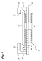
- Fig. 1 is a schematic view for explaining a cross-sectional configuration of a radiographic imaging apparatus according to an embodiment of the present invention.
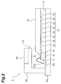
- Fig. 2 is a schematic view for explaining the cross-sectional configuration of the radiographic imaging apparatus according to the embodiment of the present invention.
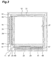
- Fig. 3 is a plan view showing the radiographic imaging apparatus according to the embodiment of the present invention.
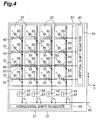
- Fig. 4 is a configuration diagram showing the radiographic imaging apparatus according to the embodiment of the present invention.
- Fig. 5 is a plan view showing a photosensitive section included in a solid-state image sensor of the radiographic imaging apparatus according to the embodiment of the present invention.
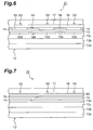
- Fig. 6 is a schematic view for explaining a cross-sectional configuration along line VI-VI in Fig. 5.
- Fig. 7 is a schematic view for explaining a cross-sectional configuration along line VII-VII in Fig. 5.
- Fig. 8 is a schematic view for explaining a cross-sectional configuration along line VIII-VIII in Fig. 5.
- Fig. 9 is a schematic view for explaining a cross-sectional configuration along line IX-IX in Fig. 5.
- a radiographic imaging apparatus incorporates a solid-state imaging apparatus (solid-state image sensor) according to an embodiment of the present invention.
- Figs. 1 and 2 are schematic views for explaining a cross-sectional configuration of the radiographic imaging apparatus according to the present embodiment
- Fig. 3 is a plan view showing the radiographic imaging apparatus according to the present embodiment
- Fig. 4 is a configuration diagram showing the radiographic imaging apparatus according to the present embodiment.
- Fig. 3 is depicted without illustration of bonding wires.
- the radiographic imaging apparatus 1 of the present embodiment has a solid-state image sensor 11, a scintillator 21, a mount substrate 23, a frame 25, and others.
- the solid-state image sensor 11 is an MOS image sensor, and has a photosensitive section 31, a shift register section 41, and an amplification section 51, which are formed on one side of a semiconductor substrate 12. In this manner, the photosensitive section 31, the shift register section 41, and the amplification section 51 are formed on the same substrate (semiconductor substrate 12).
- the semiconductor substrate 12 (solid-state image sensor 11) is fixed on the mount substrate 23.
- the photosensitive section 31 as shown in Fig. 4, is constructed in a configuration wherein a plurality of photodiodes (photoelectric converters) 33 for storing charges according to intensities of incident light are arrayed in a two-dimensional pattern on the semiconductor substrate 12. More specifically, the photosensitive section 31 is composed of M ⁇ N photodiodes 33 arrayed in a matrix of M rows in the y-axis direction and N columns in the x-axis direction (M and N are natural numbers). In Fig. 4, M and N are determined to be "4.”
- Each of the photodiodes 33 forming the photosensitive section 31 is provided with a gate switch (switch forming a first switch group) 35 one end of which is electrically connected to the photodiode 33 and the other end of which is electrically connected to a signal readout line described later. Therefore, during an opening period of the gate switch 35, a charge is stored in the photodiode 33 with incidence of light, and the charge stored in the photodiode 33 is read out to the later-described signal readout line with closure of the gate switch 35.
- the gate switch 35 can be constructed of an MOSFET (field effect transistor).
- the shift register section 41 includes a vertical shift register 43 and is formed so as to face one side of the photosensitive section 31, on the semiconductor substrate 12.
- the vertical shift register 43 outputs a vertical scan signal to open and close each gate switch 35.
- each gate switch 35 is electrically connected to the vertical shift register 43 by a gate line (second wire) 45.
- each gate switch 35 can be opened and closed by a vertical scan signal outputted from the vertical shift register 43.
- the gate lines 45 extend in the x-axis direction through portions between rows of photodiodes 33 arrayed in the photosensitive section 31, and each gate line 45 is connected to the control terminals of the respective gate switches 35 existing in one row. Accordingly, the vertical shift register 43 and the control terminals of the gate switches 35 are connected on a row-by-row basis.
- N signal readout lines (first wires; signal lines) 53, to which the other ends of the gate switches 35 are electrically connected in each column, are provided between columns of photodiodes 33 arrayed in the photosensitive section 31.
- the N signal readout lines 53 are electrically connected to the amplification section 51.
- the amplification section 51 includes charge amplifiers 55, readout switches (switches constituting a second switch group) 57, a horizontal shift register 59, and so on.
- the amplification section 51 is formed so as to face one side adjacent to the one side of the photosensitive section 31 which the shift register section 41 is formed so as to face, on the semiconductor substrate 12.
- a plurality of bonding pads 61 electrically connected to the amplifier section 51 are formed on the semiconductor substrate 12, as shown in Figs. 2 and 3. These bonding pads 61 are electrically connected to corresponding bonding pads 65 formed on the mount substrate 23, by bonding wires 63. In this configuration, the outputs from the amplification section 51 are supplied via the mount substrate 23 to the outside of the imaging apparatus 1.
- a plurality of bonding pads 67 electrically connected to the shift register section 41 are formed on the semiconductor substrate 12 (particularly, cf. Fig. 3). These bonding pads 67 are electrically connected to corresponding bonding pads 69 formed on the mount substrate 23, by bonding wires (not shown). In this configuration, signals from the outside of the imaging apparatus 1 are supplied via the mount substrate 23 to the shift register section 41.
- the scintillator 21 converts incident radiation (e.g., X-rays) to visible light and is of columnar structure.
- the scintillator 21, as also shown in Fig. 3, is arranged to cover the region where the photosensitive section 31, the shift register section 41, and the amplification section 51 are formed on one side of the semiconductor substrate 12, and is formed directly on the region. In this configuration, the scintillator 21 is arranged in contact with the region where the photosensitive section 31, the shift register section 41, and the amplification section 51 are formed on one side of the semiconductor substrate 12.
- the region where the bonding pads 61, 67 are formed on one side of the semiconductor substrate 12 is not covered by the scintillator 21, and is exposed.
- a variety of materials can be used for the scintillator 21, and one of preferred materials is Tl (thallium) doped CsI, which demonstrates good luminous efficiency.
- a protective film (not shown) for hermetically sealing the scintillator 21 while covering the columnar structure of the scintillator 21 so as to fill its gaps is formed on the scintillator 21.
- the protective film is preferably a material that transmits radiation but shields against water vapor, e.g., poly-para-xylylene (trade name Parylene, available from Three Bond Co., Ltd.), and particularly preferably, poly-para-chloroxylylene (trade name Parylene C, available from the same company).
- the thickness of the scintillator 21 is approximately 300 ⁇ m.
- the scintillator 21 can be formed by growing columnar crystals of CsI by deposition method.
- the protective film can be formed by CVD. The methods of forming the scintillator 21 and the protective film are disclosed in detail in PCT International Publication WO98/36290 filed by Applicant of the present application, for example, and the description thereof is omitted herein.
- the frame 25 is fixed on the mount substrate 23 so as to surround the solid-state image sensor 11.
- the frame 25 has an opening 27 of rectangular shape formed at the position corresponding to the photosensitive section 31, and radiation is incident through the opening 27 to the scintillator 21.
- a space S is created between the frame 25, and the semiconductor substrate 12 and the mount substrate 23.
- the shift register section 41 and the amplification section 51 of the solid-state image sensor 11, the bonding pads 61, 65, the bonding wires 63, etc. are located inside the space S. Since the bonding wires 63 are placed inside the space S defined by the frame 25, the semiconductor substrate 12, and the mount substrate 23 as described above, the bonding wires 63 are protected from external physical stress, without being pushed by the frame 25.
- a shield 29 of a radiation-shielding material (e.g., lead or the like) is provided on the side opposite to the amplification section 51 side, on the frame 25, and the shield 29 well shields against radiation.
- the thickness of the shield 29 is approximately 2.5 mm.
- Fig. 5 is a plan view showing the photosensitive section.
- Fig. 6 is a schematic view for explaining a cross-sectional configuration along line VI-VI in Fig. 5.
- Fig. 7 is a schematic view for explaining a cross-sectional configuration along line VII-VII in Fig. 5.
- Fig. 8 is a schematic view for explaining a cross-sectional configuration along line VIII-VIII in Fig. 5.
- Fig. 9 is a schematic view for explaining a cross-sectional configuration along line IX-IX in Fig. 5.
- Fig. 5 is depicted without illustration of first to fourth insulating layers 13, 15-17, and the gate switches 35.
- the semiconductor substrate 12 includes a p + -type semiconductor substrate 12a, and a p - -type epitaxial semiconductor layer 12b and a p - -type layer 12c are formed on the p + -type semiconductor substrate 12a.
- the p + -type semiconductor substrate 12a is set at the ground potential.
- the solid-state image sensor 11 is one using Si as a semiconductor; "high concentration” refers to the impurity concentration of not less than about 1 ⁇ 10 17 /cm 3 and is expressed by "+" attached to the conductivity type; “low concentration” refers to the impurity concentration of not more than about 1 ⁇ 10 15 /cm 3 and is expressed by "-" attached to the conductivity type.
- N + -type semiconductor regions 12d are formed on the front surface side of the p - -type layer 12c, and a pn junction composed of each n + -type semiconductor (n + -type semiconductor region 12d) and the p - -type semiconductor (p - -type layer 12c) constitutes a photodiode (photoelectric converter) 33.
- the n + -type semiconductor regions 12d each are of rectangular shape when viewed from the direction of incidence of light, and are arrayed in a two-dimensional pattern of M rows and N columns, as shown in Fig. 5. In this configuration, the photodiodes 33 are arrayed in the two-dimensional pattern of M rows and N columns in the photosensitive section 31.
- the length on each side of the n + -type semiconductor regions 12d is set to be approximately 50 ⁇ m.
- An isolation region 12e of a p + -type semiconductor is formed between adjacent n + -type semiconductor regions 12d on the front surface side of the p - -type layer 12c.
- the isolation region 12e as shown in Fig. 5, extends along the row direction and along the column direction between adjacent n + -type semiconductor regions 12d and is of grid shape when viewed from the direction of incidence of light.
- a first insulating layer (e.g., made of a silicon oxide film) 13 is formed on the p - -type layer 12c, the n + -type semiconductor regions 12d, and the isolation region 12e.
- a metal (e.g., aluminum) wire 14 is electrically connected to the isolation region 12e via through holes formed in the first insulating layer 13.
- the metal wire 14, as shown in Fig. 5, is provided so as to extend along the row direction and along the column direction between adjacent n + -type semiconductor regions 12d, and is of grid shape when viewed from the direction of incidence of light.
- the width of the metal wire 14 is set greater than the distance between adjacent n + -type semiconductor regions 12d, and part of the metal wire 14 overlaps the edges of n + -type semiconductor regions 12d when viewed from the direction of incidence of light.
- the metal wire 14 is grounded and thus the isolation region 12e is set at the ground potential.
- the metal wire 14 may also be connected to a fixed potential, instead of being grounded.
- a second insulating layer (e.g., made of a silicon oxide film) 15 is formed on the first insulating layer 13.
- the aforementioned gate lines 45 and a third insulating layer (e.g., made of a silicon oxide film) 16 are formed on the second insulating layer 15.
- the gate lines 45 are made of metal such as aluminum, and are provided so as to extend along the row direction and between adjacent n + -type semiconductor regions 12d.
- the aforementioned signal readout lines 53 and a fourth insulating layer (e.g., made of a silicon oxide film) 17 are formed on the third insulating layer 16.
- the signal readout lines 53 are made of metal such as aluminum, and, as shown in Figs. 5 and 6, the signal readout lines 53 are located above the n + -type semiconductor regions 12d when viewed from the direction of incidence of light, and are provided so as to extend along the column direction.
- the width of the signal readout lines 53 is set to be approximately 0.5 ⁇ m.
- the signal readout lines 53 are placed with deviation of approximately 1-20 ⁇ m from one side of n + -type semiconductor regions 12d, above the n + -type semiconductor regions 12d.
- the signal readout lines 53 are located above the n + -type semiconductor regions 12d constituting the photodiodes 33, and are thus separated from the portions between adjacent n + -type semiconductor regions 12d, i.e., from the metal wire 14. This reduces the parasitic capacitance of the signal readout lines 53 and thus suppresses generation of noise, thereby improving the SN ratio.
- the photosensitivity of the photodiodes 33 becomes lower (by about 1.6% in the present embodiment) than that in a configuration wherein the signal readout lines 53 are located between adjacent n + -type semiconductor regions 12d.
- this decrease of the photosensitivity can be compensated for by a technique of enhancing the amplification rate in the amplification section 51, or the like, whereby a decrease of image output can be prevented as a result.
- the present invention is by no means limited to the above embodiment.
- the scintillator 21 is formed directly on the semiconductor substrate 12 in the present embodiment, but the structure is not limited to this.
- a protective film is formed on the scintillator, the protective film is brought into contact with the region where the photosensitive section 31, the shift register section 41, and the amplification section 51 are formed.
Landscapes
- Measurement Of Radiation (AREA)
- Solid State Image Pick-Up Elements (AREA)
- Transforming Light Signals Into Electric Signals (AREA)
- Light Receiving Elements (AREA)
Priority Applications (1)
| Application Number | Priority Date | Filing Date | Title |
|---|---|---|---|
| EP18182005.1A EP3404719B1 (de) | 2002-11-28 | 2003-11-26 | Festkörperbildgebungsvorrichtung und röntgenbildgebungsvorrichtung |
Applications Claiming Priority (3)
| Application Number | Priority Date | Filing Date | Title |
|---|---|---|---|
| JP2002346247 | 2002-11-28 | ||
| JP2002346247A JP4391078B2 (ja) | 2002-11-28 | 2002-11-28 | 固体撮像装置及び放射線撮像装置 |
| PCT/JP2003/015108 WO2004049447A1 (ja) | 2002-11-28 | 2003-11-26 | 固体撮像装置及び放射線撮像装置 |
Related Child Applications (2)
| Application Number | Title | Priority Date | Filing Date |
|---|---|---|---|
| EP18182005.1A Division EP3404719B1 (de) | 2002-11-28 | 2003-11-26 | Festkörperbildgebungsvorrichtung und röntgenbildgebungsvorrichtung |
| EP18182005.1A Division-Into EP3404719B1 (de) | 2002-11-28 | 2003-11-26 | Festkörperbildgebungsvorrichtung und röntgenbildgebungsvorrichtung |
Publications (3)
| Publication Number | Publication Date |
|---|---|
| EP1566840A1 true EP1566840A1 (de) | 2005-08-24 |
| EP1566840A4 EP1566840A4 (de) | 2008-03-05 |
| EP1566840B1 EP1566840B1 (de) | 2018-09-05 |
Family
ID=32376050
Family Applications (2)
| Application Number | Title | Priority Date | Filing Date |
|---|---|---|---|
| EP03811935.0A Expired - Lifetime EP1566840B1 (de) | 2002-11-28 | 2003-11-26 | Röhrenlose abbildungseinrichtung und strahlungsabbildungssystem |
| EP18182005.1A Expired - Lifetime EP3404719B1 (de) | 2002-11-28 | 2003-11-26 | Festkörperbildgebungsvorrichtung und röntgenbildgebungsvorrichtung |
Family Applications After (1)
| Application Number | Title | Priority Date | Filing Date |
|---|---|---|---|
| EP18182005.1A Expired - Lifetime EP3404719B1 (de) | 2002-11-28 | 2003-11-26 | Festkörperbildgebungsvorrichtung und röntgenbildgebungsvorrichtung |
Country Status (6)
| Country | Link |
|---|---|
| US (1) | US7276683B2 (de) |
| EP (2) | EP1566840B1 (de) |
| JP (1) | JP4391078B2 (de) |
| CN (1) | CN100463198C (de) |
| AU (1) | AU2003302293A1 (de) |
| WO (1) | WO2004049447A1 (de) |
Families Citing this family (7)
| Publication number | Priority date | Publication date | Assignee | Title |
|---|---|---|---|---|
| FR2888044B1 (fr) * | 2005-07-01 | 2007-08-31 | Atmel Grenoble Soc Par Actions | Capteur d'image a coins coupes |
| US7791170B2 (en) * | 2006-07-10 | 2010-09-07 | Taiwan Semiconductor Manufacturing Company, Ltd. | Method of making a deep junction for electrical crosstalk reduction of an image sensor |
| WO2008104928A1 (en) * | 2007-03-01 | 2008-09-04 | Philips Intellectual Property & Standards Gmbh | Optical detector device |
| JP5406473B2 (ja) * | 2007-07-19 | 2014-02-05 | キヤノン株式会社 | 放射線検出装置 |
| DE102009004409A1 (de) * | 2009-01-13 | 2010-07-15 | Arnold & Richter Cine Technik Gmbh & Co. Betriebs Kg | Bildsensor |
| US9412725B2 (en) * | 2012-04-27 | 2016-08-09 | Taiwan Semiconductor Manufacturing Company, Ltd. | Method and apparatus for image sensor packaging |
| JP6530600B2 (ja) * | 2014-12-03 | 2019-06-12 | キヤノン株式会社 | 放射線検出装置及び放射線検出システム |
Family Cites Families (12)
| Publication number | Priority date | Publication date | Assignee | Title |
|---|---|---|---|---|
| JP3697769B2 (ja) * | 1995-02-24 | 2005-09-21 | 株式会社ニコン | 光電変換素子及び光電変換装置 |
| JP3486490B2 (ja) * | 1995-09-04 | 2004-01-13 | キヤノン株式会社 | 放射線検出装置 |
| JPH09238287A (ja) * | 1996-02-29 | 1997-09-09 | Nikon Corp | 固体撮像装置 |
| JP3412390B2 (ja) * | 1996-03-18 | 2003-06-03 | 株式会社ニコン | 光電変換装置 |
| DE69817035T2 (de) | 1997-02-14 | 2004-06-09 | Hamamatsu Photonics K.K., Hamamatsu | Strahlungsdetektor und Verfahren zu seiner Herstellung |
| JP3869952B2 (ja) * | 1998-09-21 | 2007-01-17 | キヤノン株式会社 | 光電変換装置とそれを用いたx線撮像装置 |
| JP4812940B2 (ja) * | 1998-10-30 | 2011-11-09 | 浜松ホトニクス株式会社 | 固体撮像装置アレイ |
| TW494574B (en) * | 1999-12-01 | 2002-07-11 | Innotech Corp | Solid state imaging device, method of manufacturing the same, and solid state imaging system |
| JP4398065B2 (ja) * | 2000-05-19 | 2010-01-13 | 浜松ホトニクス株式会社 | 放射線検出器 |
| US6717151B2 (en) * | 2000-07-10 | 2004-04-06 | Canon Kabushiki Kaisha | Image pickup apparatus |
| JP2002252341A (ja) * | 2001-02-23 | 2002-09-06 | Fuji Film Microdevices Co Ltd | 固体撮像装置 |
| US6847039B2 (en) * | 2001-03-28 | 2005-01-25 | Canon Kabushiki Kaisha | Photodetecting device, radiation detecting device, and radiation imaging system |
-
2002
- 2002-11-28 JP JP2002346247A patent/JP4391078B2/ja not_active Expired - Fee Related
-
2003
- 2003-11-26 CN CNB200380104620XA patent/CN100463198C/zh not_active Expired - Lifetime
- 2003-11-26 EP EP03811935.0A patent/EP1566840B1/de not_active Expired - Lifetime
- 2003-11-26 WO PCT/JP2003/015108 patent/WO2004049447A1/ja not_active Ceased
- 2003-11-26 AU AU2003302293A patent/AU2003302293A1/en not_active Abandoned
- 2003-11-26 US US10/536,319 patent/US7276683B2/en not_active Expired - Lifetime
- 2003-11-26 EP EP18182005.1A patent/EP3404719B1/de not_active Expired - Lifetime
Also Published As
| Publication number | Publication date |
|---|---|
| CN1720619A (zh) | 2006-01-11 |
| AU2003302293A1 (en) | 2004-06-18 |
| CN100463198C (zh) | 2009-02-18 |
| US7276683B2 (en) | 2007-10-02 |
| JP2004179537A (ja) | 2004-06-24 |
| EP3404719B1 (de) | 2022-01-19 |
| EP3404719A1 (de) | 2018-11-21 |
| JP4391078B2 (ja) | 2009-12-24 |
| EP1566840B1 (de) | 2018-09-05 |
| US20060138337A1 (en) | 2006-06-29 |
| EP1566840A4 (de) | 2008-03-05 |
| WO2004049447A1 (ja) | 2004-06-10 |
Similar Documents
| Publication | Publication Date | Title |
|---|---|---|
| JP5196739B2 (ja) | 放射線撮像装置及び放射線撮像システム | |
| US20100054418A1 (en) | X-ray detecting element | |
| US7105829B2 (en) | Radiation detector having radiation sensitive semiconductor | |
| US10130317B2 (en) | Intraoral dental radiological imaging sensor | |
| CN103999220A (zh) | 传感器单元以及固体摄像装置 | |
| US7276683B2 (en) | Solid-state imaging device and radiation imaging system | |
| US7372037B2 (en) | Solid-state imaging device and radiotion imaging system | |
| CN101390213B (zh) | 放射线检测器 | |
| JP4455534B2 (ja) | 放射線検出器およびその製造方法 | |
| US7432509B2 (en) | Radiographic imaging system | |
| US20040173754A1 (en) | X-ray imager | |
| JP4326021B2 (ja) | 電荷結合撮像装置 | |
| JP2004177217A (ja) | 放射線撮像装置 | |
| EP1801877B1 (de) | Verfahren zur Herstellung eines Röntgendetektors | |
| JP4315593B2 (ja) | 半導体撮像装置および撮像システム | |
| JP2002124655A (ja) | 電磁波電気信号変換システム及びイメージセンサ | |
| JP3304857B2 (ja) | 放射線撮像装置 |
Legal Events
| Date | Code | Title | Description |
|---|---|---|---|
| PUAI | Public reference made under article 153(3) epc to a published international application that has entered the european phase |
Free format text: ORIGINAL CODE: 0009012 |
|
| 17P | Request for examination filed |
Effective date: 20050613 |
|
| AK | Designated contracting states |
Kind code of ref document: A1 Designated state(s): AT BE BG CH CY CZ DE DK EE ES FI FR GB GR HU IE IT LI LU MC NL PT RO SE SI SK TR |
|
| AX | Request for extension of the european patent |
Extension state: AL LT LV MK |
|
| DAX | Request for extension of the european patent (deleted) | ||
| RBV | Designated contracting states (corrected) |
Designated state(s): CH DE FR GB IT LI |
|
| A4 | Supplementary search report drawn up and despatched |
Effective date: 20080201 |
|
| 17Q | First examination report despatched |
Effective date: 20080312 |
|
| STAA | Information on the status of an ep patent application or granted ep patent |
Free format text: STATUS: EXAMINATION IS IN PROGRESS |
|
| GRAP | Despatch of communication of intention to grant a patent |
Free format text: ORIGINAL CODE: EPIDOSNIGR1 |
|
| STAA | Information on the status of an ep patent application or granted ep patent |
Free format text: STATUS: GRANT OF PATENT IS INTENDED |
|
| INTG | Intention to grant announced |
Effective date: 20180327 |
|
| GRAS | Grant fee paid |
Free format text: ORIGINAL CODE: EPIDOSNIGR3 |
|
| GRAA | (expected) grant |
Free format text: ORIGINAL CODE: 0009210 |
|
| STAA | Information on the status of an ep patent application or granted ep patent |
Free format text: STATUS: THE PATENT HAS BEEN GRANTED |
|
| AK | Designated contracting states |
Kind code of ref document: B1 Designated state(s): CH DE FR GB IT LI |
|
| REG | Reference to a national code |
Ref country code: GB Ref legal event code: FG4D |
|
| REG | Reference to a national code |
Ref country code: CH Ref legal event code: EP |
|
| REG | Reference to a national code |
Ref country code: CH Ref legal event code: NV Representative=s name: SERVOPATENT GMBH, CH |
|
| REG | Reference to a national code |
Ref country code: DE Ref legal event code: R096 Ref document number: 60351450 Country of ref document: DE |
|
| REG | Reference to a national code |
Ref country code: FR Ref legal event code: PLFP Year of fee payment: 16 |
|
| REG | Reference to a national code |
Ref country code: CH Ref legal event code: PK Free format text: BERICHTIGUNGEN |
|
| RIC2 | Information provided on ipc code assigned after grant |
Ipc: G01T 1/24 20060101ALI20040615BHEP Ipc: H01L 27/146 20060101AFI20040615BHEP |
|
| REG | Reference to a national code |
Ref country code: DE Ref legal event code: R097 Ref document number: 60351450 Country of ref document: DE |
|
| PLBE | No opposition filed within time limit |
Free format text: ORIGINAL CODE: 0009261 |
|
| STAA | Information on the status of an ep patent application or granted ep patent |
Free format text: STATUS: NO OPPOSITION FILED WITHIN TIME LIMIT |
|
| 26N | No opposition filed |
Effective date: 20190606 |
|
| REG | Reference to a national code |
Ref country code: CH Ref legal event code: PCAR Free format text: NEW ADDRESS: WANNERSTRASSE 9/1, 8045 ZUERICH (CH) |
|
| PGFP | Annual fee paid to national office [announced via postgrant information from national office to epo] |
Ref country code: DE Payment date: 20201110 Year of fee payment: 18 Ref country code: GB Payment date: 20201118 Year of fee payment: 18 Ref country code: FR Payment date: 20201013 Year of fee payment: 18 Ref country code: IT Payment date: 20201013 Year of fee payment: 18 Ref country code: CH Payment date: 20201117 Year of fee payment: 18 |
|
| REG | Reference to a national code |
Ref country code: DE Ref legal event code: R119 Ref document number: 60351450 Country of ref document: DE |
|
| REG | Reference to a national code |
Ref country code: CH Ref legal event code: PL |
|
| GBPC | Gb: european patent ceased through non-payment of renewal fee |
Effective date: 20211126 |
|
| PG25 | Lapsed in a contracting state [announced via postgrant information from national office to epo] |
Ref country code: GB Free format text: LAPSE BECAUSE OF NON-PAYMENT OF DUE FEES Effective date: 20211126 Ref country code: DE Free format text: LAPSE BECAUSE OF NON-PAYMENT OF DUE FEES Effective date: 20220601 |
|
| PG25 | Lapsed in a contracting state [announced via postgrant information from national office to epo] |
Ref country code: FR Free format text: LAPSE BECAUSE OF NON-PAYMENT OF DUE FEES Effective date: 20211130 |
|
| PG25 | Lapsed in a contracting state [announced via postgrant information from national office to epo] |
Ref country code: IT Free format text: LAPSE BECAUSE OF NON-PAYMENT OF DUE FEES Effective date: 20211126 |
|
| PG25 | Lapsed in a contracting state [announced via postgrant information from national office to epo] |
Ref country code: LI Free format text: LAPSE BECAUSE OF NON-PAYMENT OF DUE FEES Effective date: 20220630 Ref country code: CH Free format text: LAPSE BECAUSE OF NON-PAYMENT OF DUE FEES Effective date: 20220630 |