EP1566675A1 - Optischer Sender-Empfänger und optisches Modul dafür - Google Patents
Optischer Sender-Empfänger und optisches Modul dafür Download PDFInfo
- Publication number
- EP1566675A1 EP1566675A1 EP05251073A EP05251073A EP1566675A1 EP 1566675 A1 EP1566675 A1 EP 1566675A1 EP 05251073 A EP05251073 A EP 05251073A EP 05251073 A EP05251073 A EP 05251073A EP 1566675 A1 EP1566675 A1 EP 1566675A1
- Authority
- EP
- European Patent Office
- Prior art keywords
- optical
- light
- main housing
- optical module
- emitting component
- Prior art date
- Legal status (The legal status is an assumption and is not a legal conclusion. Google has not performed a legal analysis and makes no representation as to the accuracy of the status listed.)
- Withdrawn
Links
- 230000003287 optical effect Effects 0.000 title claims abstract description 144
- 239000013307 optical fiber Substances 0.000 claims abstract description 46
- 230000001788 irregular Effects 0.000 claims abstract description 33
- 239000003795 chemical substances by application Substances 0.000 claims description 18
- 239000000565 sealant Substances 0.000 claims description 12
- 239000010949 copper Substances 0.000 claims description 8
- 239000000463 material Substances 0.000 claims description 7
- 229920001296 polysiloxane Polymers 0.000 claims description 7
- 229920005989 resin Polymers 0.000 claims description 7
- 239000011347 resin Substances 0.000 claims description 7
- RYGMFSIKBFXOCR-UHFFFAOYSA-N Copper Chemical compound [Cu] RYGMFSIKBFXOCR-UHFFFAOYSA-N 0.000 claims description 5
- PIGFYZPCRLYGLF-UHFFFAOYSA-N Aluminum nitride Chemical compound [Al]#N PIGFYZPCRLYGLF-UHFFFAOYSA-N 0.000 claims description 4
- LTPBRCUWZOMYOC-UHFFFAOYSA-N Beryllium oxide Chemical compound O=[Be] LTPBRCUWZOMYOC-UHFFFAOYSA-N 0.000 claims description 4
- OKTJSMMVPCPJKN-UHFFFAOYSA-N Carbon Chemical compound [C] OKTJSMMVPCPJKN-UHFFFAOYSA-N 0.000 claims description 4
- BQCADISMDOOEFD-UHFFFAOYSA-N Silver Chemical compound [Ag] BQCADISMDOOEFD-UHFFFAOYSA-N 0.000 claims description 4
- 229910052782 aluminium Inorganic materials 0.000 claims description 4
- XAGFODPZIPBFFR-UHFFFAOYSA-N aluminium Chemical compound [Al] XAGFODPZIPBFFR-UHFFFAOYSA-N 0.000 claims description 4
- 229910052799 carbon Inorganic materials 0.000 claims description 4
- 229910052802 copper Inorganic materials 0.000 claims description 4
- 229910003460 diamond Inorganic materials 0.000 claims description 4
- 239000010432 diamond Substances 0.000 claims description 4
- HBMJWWWQQXIZIP-UHFFFAOYSA-N silicon carbide Chemical compound [Si+]#[C-] HBMJWWWQQXIZIP-UHFFFAOYSA-N 0.000 claims description 4
- 229910052709 silver Inorganic materials 0.000 claims description 4
- 239000004332 silver Substances 0.000 claims description 4
- 239000002245 particle Substances 0.000 claims description 3
- 230000017525 heat dissipation Effects 0.000 abstract description 17
- 239000000853 adhesive Substances 0.000 abstract description 8
- 230000001070 adhesive effect Effects 0.000 abstract description 8
- 230000015556 catabolic process Effects 0.000 abstract description 3
- 238000006731 degradation reaction Methods 0.000 abstract description 3
- 239000000835 fiber Substances 0.000 description 8
- 230000001965 increasing effect Effects 0.000 description 8
- PXHVJJICTQNCMI-UHFFFAOYSA-N Nickel Chemical compound [Ni] PXHVJJICTQNCMI-UHFFFAOYSA-N 0.000 description 3
- 230000005540 biological transmission Effects 0.000 description 3
- 238000003754 machining Methods 0.000 description 3
- 229910052751 metal Inorganic materials 0.000 description 3
- 239000002184 metal Substances 0.000 description 3
- 230000007175 bidirectional communication Effects 0.000 description 2
- 239000012141 concentrate Substances 0.000 description 2
- 230000002708 enhancing effect Effects 0.000 description 2
- 239000010931 gold Substances 0.000 description 2
- 238000012986 modification Methods 0.000 description 2
- 230000004048 modification Effects 0.000 description 2
- 230000008054 signal transmission Effects 0.000 description 2
- 238000003466 welding Methods 0.000 description 2
- XEEYBQQBJWHFJM-UHFFFAOYSA-N Iron Chemical compound [Fe] XEEYBQQBJWHFJM-UHFFFAOYSA-N 0.000 description 1
- 239000000654 additive Substances 0.000 description 1
- 230000000996 additive effect Effects 0.000 description 1
- 230000015572 biosynthetic process Effects 0.000 description 1
- 238000006243 chemical reaction Methods 0.000 description 1
- 230000006854 communication Effects 0.000 description 1
- 238000004891 communication Methods 0.000 description 1
- 230000008878 coupling Effects 0.000 description 1
- 238000010168 coupling process Methods 0.000 description 1
- 238000005859 coupling reaction Methods 0.000 description 1
- 230000007423 decrease Effects 0.000 description 1
- 230000003247 decreasing effect Effects 0.000 description 1
- 230000000694 effects Effects 0.000 description 1
- 239000003822 epoxy resin Substances 0.000 description 1
- PCHJSUWPFVWCPO-UHFFFAOYSA-N gold Chemical compound [Au] PCHJSUWPFVWCPO-UHFFFAOYSA-N 0.000 description 1
- 229910052737 gold Inorganic materials 0.000 description 1
- 238000010348 incorporation Methods 0.000 description 1
- 239000011159 matrix material Substances 0.000 description 1
- 229910052759 nickel Inorganic materials 0.000 description 1
- 230000002093 peripheral effect Effects 0.000 description 1
- 229920000647 polyepoxide Polymers 0.000 description 1
- 229920002050 silicone resin Polymers 0.000 description 1
Images




Classifications
-
- G—PHYSICS
- G02—OPTICS
- G02B—OPTICAL ELEMENTS, SYSTEMS OR APPARATUS
- G02B6/00—Light guides; Structural details of arrangements comprising light guides and other optical elements, e.g. couplings
- G02B6/24—Coupling light guides
- G02B6/42—Coupling light guides with opto-electronic elements
- G02B6/4201—Packages, e.g. shape, construction, internal or external details
-
- G—PHYSICS
- G02—OPTICS
- G02B—OPTICAL ELEMENTS, SYSTEMS OR APPARATUS
- G02B6/00—Light guides; Structural details of arrangements comprising light guides and other optical elements, e.g. couplings
- G02B6/24—Coupling light guides
- G02B6/42—Coupling light guides with opto-electronic elements
- G02B6/4201—Packages, e.g. shape, construction, internal or external details
- G02B6/4204—Packages, e.g. shape, construction, internal or external details the coupling comprising intermediate optical elements, e.g. lenses, holograms
- G02B6/4214—Packages, e.g. shape, construction, internal or external details the coupling comprising intermediate optical elements, e.g. lenses, holograms the intermediate optical element having redirecting reflective means, e.g. mirrors, prisms for deflecting the radiation from horizontal to down- or upward direction toward a device
-
- G—PHYSICS
- G02—OPTICS
- G02B—OPTICAL ELEMENTS, SYSTEMS OR APPARATUS
- G02B6/00—Light guides; Structural details of arrangements comprising light guides and other optical elements, e.g. couplings
- G02B6/24—Coupling light guides
- G02B6/42—Coupling light guides with opto-electronic elements
- G02B6/4201—Packages, e.g. shape, construction, internal or external details
- G02B6/4246—Bidirectionally operating package structures
-
- G—PHYSICS
- G02—OPTICS
- G02B—OPTICAL ELEMENTS, SYSTEMS OR APPARATUS
- G02B6/00—Light guides; Structural details of arrangements comprising light guides and other optical elements, e.g. couplings
- G02B6/24—Coupling light guides
- G02B6/42—Coupling light guides with opto-electronic elements
- G02B6/4201—Packages, e.g. shape, construction, internal or external details
- G02B6/4256—Details of housings
-
- G—PHYSICS
- G02—OPTICS
- G02B—OPTICAL ELEMENTS, SYSTEMS OR APPARATUS
- G02B6/00—Light guides; Structural details of arrangements comprising light guides and other optical elements, e.g. couplings
- G02B6/24—Coupling light guides
- G02B6/42—Coupling light guides with opto-electronic elements
- G02B6/4201—Packages, e.g. shape, construction, internal or external details
- G02B6/4266—Thermal aspects, temperature control or temperature monitoring
- G02B6/4268—Cooling
- G02B6/4269—Cooling with heat sinks or radiation fins
-
- G—PHYSICS
- G02—OPTICS
- G02B—OPTICAL ELEMENTS, SYSTEMS OR APPARATUS
- G02B6/00—Light guides; Structural details of arrangements comprising light guides and other optical elements, e.g. couplings
- G02B6/24—Coupling light guides
- G02B6/42—Coupling light guides with opto-electronic elements
- G02B6/4201—Packages, e.g. shape, construction, internal or external details
- G02B6/4204—Packages, e.g. shape, construction, internal or external details the coupling comprising intermediate optical elements, e.g. lenses, holograms
-
- G—PHYSICS
- G02—OPTICS
- G02B—OPTICAL ELEMENTS, SYSTEMS OR APPARATUS
- G02B6/00—Light guides; Structural details of arrangements comprising light guides and other optical elements, e.g. couplings
- G02B6/24—Coupling light guides
- G02B6/42—Coupling light guides with opto-electronic elements
- G02B6/4201—Packages, e.g. shape, construction, internal or external details
- G02B6/4219—Mechanical fixtures for holding or positioning the elements relative to each other in the couplings; Alignment methods for the elements, e.g. measuring or observing methods especially used therefor
- G02B6/422—Active alignment, i.e. moving the elements in response to the detected degree of coupling or position of the elements
-
- G—PHYSICS
- G02—OPTICS
- G02B—OPTICAL ELEMENTS, SYSTEMS OR APPARATUS
- G02B6/00—Light guides; Structural details of arrangements comprising light guides and other optical elements, e.g. couplings
- G02B6/24—Coupling light guides
- G02B6/42—Coupling light guides with opto-electronic elements
- G02B6/4201—Packages, e.g. shape, construction, internal or external details
- G02B6/4219—Mechanical fixtures for holding or positioning the elements relative to each other in the couplings; Alignment methods for the elements, e.g. measuring or observing methods especially used therefor
- G02B6/4236—Fixing or mounting methods of the aligned elements
- G02B6/4237—Welding
-
- G—PHYSICS
- G02—OPTICS
- G02B—OPTICAL ELEMENTS, SYSTEMS OR APPARATUS
- G02B6/00—Light guides; Structural details of arrangements comprising light guides and other optical elements, e.g. couplings
- G02B6/24—Coupling light guides
- G02B6/42—Coupling light guides with opto-electronic elements
- G02B6/4201—Packages, e.g. shape, construction, internal or external details
- G02B6/4219—Mechanical fixtures for holding or positioning the elements relative to each other in the couplings; Alignment methods for the elements, e.g. measuring or observing methods especially used therefor
- G02B6/4236—Fixing or mounting methods of the aligned elements
- G02B6/4239—Adhesive bonding; Encapsulation with polymer material
Definitions
- the present invention relates to an optical transceiver and to an optical module used in the transceiver. It particularly relates to an optical transceiver that can be used for bi-directional communication system, and to an optical module used in the optical transceiver.
- an optical module has to be used between an optical fiber and a terminal in order to connect the optical fiber to the terminal.
- An optical module is a device that converts optical signals received from the optical fiber to electric signals and supplies the electric signals to the terminal, and converts electric signals from the terminal to optical signals that are supplied to the optical fiber.
- various types of optical module have been proposed.
- Optical output level is an important parameter indicating optical module performance.
- High-speed data communication systems require high output levels.
- PON passive optical network
- a 1 GB/sec PON system requires an output level of at least around -1 dBm after a transmission of 20 km.
- Optical output levels can be effectively increased by using light-emitting components that have a high luminous efficiency or by improving a coupling efficiency between the light-emitting component and the optical fiber, but it difficult to obtain a sufficiently high output level by doing just that.
- Another object of the present invention is to provide an optical module that enables drive current to light-emitting components to be reduced, thereby improving reliability, and an optical transceiver that includes the optical module.
- an optical module to be employed to an optical transceiver, for converting an optical signal received from an optical fiber into an electronic signal and converting the electronic signal into the optical signal to be supplied to the optical fiber, comprising:
- the optical module itself has a very high heat dissipation property, eliminating the type of problems that arise when adhesive or the like is used to attach to the main housing heat sinks constituted as separate parts, such as the increase in the number of parts and the degradation in thermal conductivity to the heat sink caused by the adhesive.
- the irregular pattern is formed in a vicinity of the light emitter component. This is because among the components constituting an optical module, the light-emitting component generates the most heat.
- the irregular pattern can be composed of a plurality of heat-dissipating fins or a plurality of heat-dissipating rods.
- the optical module further comprises a sealant to seal a gap between the main housing and the light-emitting component, a main component of the sealant being a resin including an agent to enhance a thermal conductivity.
- a thermal conductivity of the agent is equal to or more than 200 W/(m ⁇ °C). It is further preferable that the agent is in a form of particles having a diameter that is 0.1 to 20 ⁇ m.
- the agent includes at least one of materials selected from a group of copper (Cu), silver (Ag), aluminum (Al), aluminum nitride (AlN), beryllium oxide (BeO), silicon carbide (SiC), diamond and diamond-like carbon.
- materials selected from a group of copper (Cu), silver (Ag), aluminum (Al), aluminum nitride (AlN), beryllium oxide (BeO), silicon carbide (SiC), diamond and diamond-like carbon.
- the optical module further comprises:
- the two optical filters are held by just the one filter support member, it is possible to keep down the number of parts. Moreover, having the two optical filters held by the one filter support member also provides good positioning accuracy, since there is almost no deviation in the positional relationship of the two filters.
- the first optical filter can reflect a light supplied from the optical fiber and can transmit a light emitted from the light-emitting component
- the second optical filter can transmit a light supplied from the optical fiber and can reflect a light emitted from the light-emitting component.
- an optical transceiver comprising an electronic circuit formed on a circuit board and an optical module for converting an optical signal received from an optical fiber into an electronic signal to be supplied to the electronic circuit and converting the electronic signal received from the electronic circuit into the optical signal to be supplied to the optical fiber, the optical module, comprising:
- At least part of the main housing comprises a heat sink, giving the optical module itself a very high heat dissipation property without increasing the number of parts.
- the circuit board has a cut portion to prevent the circuit board from covering the irregular pattern of the main housing. According to this aspect of the present invention, because the irregular pattern is exposed rather than being covered by the circuit board, so heat dissipation by the irregular pattern is not obstructed by the circuit board.
- the optical transceiver further comprises a transceiver case for supporting the circuit board and the optical module and a silicone gel provided between the transceiver case and the main housing.
- the heat of the main housing can be efficiently conducted to the transceiver case, further enhancing the heat dissipation property.
- the silicone gel includes an agent to enhance a thermal conductivity.
- the optical module itself has a very high heat-dissipation property, effectively holding in check the temperature elevation of the light-emitting component. This enables the drive current to the light-emitting component to be reduced, thereby increasing the reliability of the product.
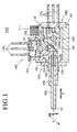
- Figure 1 is a cross-sectional view of the configuration of an optical module 100 according to a preferred embodiment of the present invention.
- the optical module 100 includes a main housing 110, a fiber support component 120 affixed to the main housing 110, a light-emitting component 130, a light-receiving component 140, a filter support member 150 provided so that it covers the light-receiving component 140, and first and second optical filters 161 and 162 that are held by the filter support member 150.
- the optical module 100 is used to carry out bi-directional communication between terminals using optical signals.
- the optical module 100 does this by receiving optical signals from an optical fiber 121 that have a wavelength of, for example, about 1500 nm and converting them to electric signals, and converting electric signals from a terminal to optical signals that have a wavelength of, for example, about 1300 nm, and supplying the optical signals to the optical fiber 121.
- the main housing 110 is in the form of a cylindrical structure having the fiber support component 120 attached to one end and the light-emitting component 130 attached to the other end.
- the light-receiving component 140 is affixed at an angle of 90 degrees to a straight line connecting the fiber support component 120 and the light-emitting component 130.
- Metal is the optimum material for the main housing 110.
- a part of the surface of the main housing 110 has an irregular pattern 111 that improve heat dissipation.
- a part of the main housing 110 constitutes a heat sink, so the optical module 100 itself has a very high heat dissipation property, eliminating the type of problems that arise when adhesive or the like is used to attach separate heat sink components to the main housing 110, such as the increase in the number of parts and the degradation in thermal conductivity to the heat sink caused by the adhesive.
- the irregular pattern 111 are provided in the vicinity of the light-emitting component 130. This is because of the components constituting the optical module 100, the light-emitting component 130 generates the most heat, and with this arrangement, the heat generated by the light-emitting component 130 is efficiently dissipated to the outside by the irregular pattern 111.
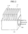
- Figure 2 is an enlarged perspective view of the portion of the main housing 110 forming the irregular pattern 111.
- the irregular pattern 111 comprise a regular array of a plurality of heat-dissipation fins 111a which increase the surface area of the main housing 110.
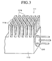
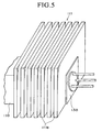
- the shape of the irregular pattern 111 is not limitative. Instead, the irregular pattern 111 can be formed as a regular array of a plurality of square heat-dissipating rods 111b, as shown in Figure 3, or round heat-dissipating rods 111c, as shown in Figure 4. It is also not necessary to arrange the heat-dissipating fins 111a or the heat-dissipating rods 111b in a regular array. Any formation may be used that increases the surface area of the main housing 110. Moreover, although in Figures 2 to 4 the irregular pattern 111 are shown as being provided on one surface of the main housing 110, this is not limitative.
- the irregular pattern 111 may be provided on two or more surfaces of the main housing 110, as long as it does not interfere with the incorporation to the optical transceiver described below. This does not mean the main housing 110 has to have a square shape; it can instead be round.
- the fiber support component 120 is attached in one end of the main housing 110.
- the fiber support component 120 functions by holding the end of the optical fiber 121 as the optical signal transmission medium, and the optical fiber cover 122.
- the fiber support component 120 includes a ring-shaped first slider 123, and a cylindrical second slider 124 into which is inserted a ferrule 125 that holds the end portion of the optical fiber 121.
- the first slider 123 can slidably move in the X direction (vertically with respect to Figure 1) and the Y direction (normal to the page on which Figure 1 is drawn), which allows the position of the optical fiber 121 to be adjusted perpendicularly to the optical axis.
- the second slider 124 can slidably move in the Z direction (from side to side with respect to Figure 1) relative to the first slider 123, which allows the position of the optical fiber 121 to be adjusted along the line of the optical axis. While there is no particular limitation on the material of the first and second sliders 123 and 124, from the standpoint of mechanical strength and machining precision, it is preferable to use metal.
- the light-emitting component 130 is attached in the other end the main housing 110.
- the light-emitting component 130 includes a light-emitting portion 131, a lens 132 that concentrates the transmitting light 100a emitted by the light-emitting portion 131, and signal pins 133 that receive the electric signals from a terminal.
- the function of the light-emitting component 130 is to use the light-emitting portion 131 to convert an electric signal received from the terminal via the signal pins 133 into an optical signal, and transmit the optical signal to the optical fiber 121, via the lens 132.
- the lens 132 is not an essential component of the light-emitting component 130, and may therefore be omitted.
- Figure 6 is an enlarged partial cross-sectional view of the vicinity of the light-emitting component 130 of the optical module 100.
- the light-emitting portion 131 of the light-emitting component 130 comprises a platform 131a extending from a stem 130a, a sub-mount 131b mounted on the platform 131a, and a laser diode 131c mounted on the sub-mount 131b.
- the actual photoelectric conversion is carried out by the laser diode 131c.
- the platform 131a and the sub-mount 131b are provided to support the laser diode 131c. Heat produced by the laser diode 131c is conducted to the main housing 110 via the sub-mount 131b, platform 131a and stem 130a, and is dissipated to the outside mainly by the irregular pattern 111.
- the stem 130a is affixed to the main housing 110 by a welded portion 134.
- the gap between the main housing 110 and the light-emitting component 130 is sealed with a sealant 135.
- the welded portion 134 can be formed by laser welding or resistance welding or the like.
- the sealant 135 Since the gap between the light-emitting component 130 and the main housing 110 is filled with the sealant 135, if the sealant 135 has low thermal conductivity, heat generated by the laser diode 131c will not be efficiently conducted to the main housing 110.
- an agent is added to the resin which is the main component of the sealant 135, to increase the thermal conductivity of the sealant.
- the resin may be epoxy resin or silicone resin or the like.
- the agent used to increase the thermal conductivity has to have a higher thermal conductivity than that of the resin, and preferably has a thermal conductivity that is higher than the 50 W/(m ⁇ °C) or more of the iron (Fe) which is the preferred material of the main housing 110.
- the agent should have a thermal conductivity of at least 200 W/(m ⁇ °C).
- the agent should also be in the form of particles having a diameter that is not less than 0.1 ⁇ m and not more than 20 ⁇ m. A particulate size in that range enables the agent to be evenly distributed in the resin without any major loss of the close adhesive power of the sealant 135.
- the agent used to enhance the thermal conductivity should include one or more selected from the group copper (Cu), silver (Ag), aluminum (Al), aluminum nitride (AlN), beryllium oxide (BeO), silicon carbide (SiC), diamond and diamond-like carbon.
- Copper (Cu) has a thermal conductivity of 400 W/(m ⁇ °C); that of silver (Ag) is 428 W/(m ⁇ °C); that of aluminum (Al) is 237 W/(m ⁇ °C); that of aluminum nitride (AlN) is 285 W/(m ⁇ °C); that of beryllium oxide (BeO) is 330 W/(m ⁇ °C); and that of silicon carbide (SiC) is 400 W/(m ⁇ °C) (values differ depending on the structure); diamond and diamond-like carbon has a thermal conductivity of 620 W/(m ⁇ °C).
- the particulate matrix of the above agents may be coated with nickel (Ni) or gold (Au).
- the light-receiving component 140 includes a light-receiving element 141, such as a photodiode or the like, a lens 142 that concentrates the receiving light 100b from the optical fiber 121 to the light-receiving element 141, and signal pins 143 that supply electric signals to a terminal.
- the function of the light-receiving component 140 is to use the light-receiving element 141 to convert an optical signal received via the lens 142 into an electric signal, and transmit the electric signal to the terminal, via the signal pins 143.
- the lens 142 is not an essential component of the light-emitting component 140, and may therefore be omitted.
- Figure 7 is a perspective view showing the structure of the filter support member 150 in more detail.
- the filter support member 150 comprises a first cylindrical portion 151, a second cylindrical portion 152 having a smaller diameter than that of the first cylindrical portion 151, a stop portion 153 that connects the first and second cylindrical portions 151 and 152, a filter mounting portion 154 with an opening 154a provided at one end of the second cylindrical portion 152, and first and second projecting portions 155 and 156 provided on the filter mounting portion 154.
- the first cylindrical portion 151, second cylindrical portion 152, stop portion 153 and filter mounting portion 154 comprise a cap portion.
- the cap portion of the filter support member 150 is set into the main housing 110, and the light-receiving component 140 is set into the cap portion. Therefore, when the light-receiving component 140 and filter support member 150 are held by the main housing 110, the first cylindrical portion 151 is set between the main housing 110 and the light-receiving component 140.
- the stop portion 153 acts as a stop to the inserted light-receiving component 140, so that the light-receiving component 140 is accurately positioned with respect to the filter support member 150.
- the first and second projecting portions 155 and 156 are curved parts formed by cutting a section of a cylinder, and are arranged on either side of the path of the transmitting light 100a. This enables the transmitting light 100a from the light-emitting component 130 to be supplied to the optical fiber 121 without being blocked by the filter support member 150.
- the first and second projecting portions 155 and 156 each has a surface (first surface) 157 that is at an angle of 45 degrees to the path of the transmitting light 100a.
- the first optical filter 161 is maintained on this first surface 157.
- the filter mounting portion 154 also has a surface (second surface) 158 that is substantially perpendicular to the light-receiving component 140, and on which the second optical filter 162 is maintained.
- the first optical filter 161 reflects the receiving light 100b from the optical fiber 121 and transmits the transmitting light 100a from the light-emitting component 130.
- the second optical filter 162 transmits the receiving light 100b from the optical fiber 121 and reflects the transmitting light 100a from the light-emitting component 130. Therefore, while the transmitting light 100a produced by the light-emitting component 130 is transmitted by the first optical filter 161 to the optical fiber 121, the receiving light 100b from the optical fiber 121 is reflected by the first optical filter 161, changing the path 90 degrees, after which the light falls substantially perpendicularly incident on the second optical filter 162 and is thereby transmitted to the light-receiving component 140.
- the optical module 100 of this embodiment having the above-described configuration, since a part of the surface of the main housing 110 has the irregular pattern 111 to increase the heat-dissipating property, heat generated by the light-emitting component 130 can be effectively exhausted without increasing the number of parts. Also, an additive is used to improve the thermal conductivity of the resin that is the main component of the sealant 135, ensuring that the heat generated by the light-emitting component 130 is efficiently conducted to the main housing 110. Thus, since in the optical module 100 of this embodiment the temperature elevation of the light-emitting component 130 is effectively avoided, the drive current to the light-emitting component 130 can be decreased, increasing the product reliability.
- the two optical filters 161 and 162 are held by just the one filter support member 150, it is possible to keep down the number of parts. Having the two optical filters 161 and 162 held by the one filter support member 150 also provides good positioning accuracy, since there is almost no deviation in the positional relationship of the two filters.
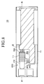
- Figure 8 is a plan view of an optical transceiver 10 that is a preferred embodiment of the present invention.
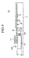
- Figure 9 is a cross-sectional view along line A-A of Figure 8.
- the optical transceiver 10 of this embodiment comprises a transceiver case 11, a printed circuit board 12, and optical module 100 supported by the transceiver case 11.
- Formed on the printed circuit board 12 is an electronic circuit composed of a plurality of electronic components 13 and the like. Electric signals supplied by the optical module 100 and electric signals to be supplied to the optical module 100 are processed by this electronic circuit.
- a cut portion 12a is formed on the printed circuit board 12 corresponding to the optical module 100. This ensures that the irregular pattern 111 are exposed rather than being covered by the circuit board 12, so heat dissipation by the irregular pattern 111 is not obstructed by the circuit board 12. Note that it is not necessary to expose entire of the optical module 100 via the cut portion 12a.
- the cut portion 12a of the printed circuit board 12 should be formed corresponding to at least the irregular pattern 111.
- silicone gel 14 is provided between the main housing 110 and the transceiver case 11. This ensures that the heat of the main housing 110 is efficiently conducted to the transceiver case 11, thereby further enhancing the heat dissipation property. Because the silicone gel 14 hardens at a relatively low temperature, so the electronic components 13 and the like are not damaged during thermal hardening. It is preferable to add a agent that increases the thermal conductivity of the silicone gel 14. The same agent can be used that is used to raise the thermal conductivity of the sealant 135.
- the optical transceiver 10 has a structure that enables the heat of the optical module 100 to be efficiently dissipated. Making it possible effectively keep the temperature elevation of the light-emitting component 130 in check.
- Figure 10 is a cross-sectional view of the configuration of an optical module 200 according to another preferred embodiment of the present invention.
- the optical module 200 includes a main housing 210, a filter support component 220 affixed to the main housing 210, a light-emitting component 130, a light-receiving component 140, and first and second optical filters 261 and 262 that are held by the filter support component 220.
- the main housing 210 is in the form of a cylindrical structure having the fiber support component 220 attached to one end and the light-emitting component 130 attached to the other end.
- the light-receiving component 140 is affixed at an angle of 90 degrees to a straight line connecting the fiber support component 220 and the light-emitting component 130.
- the light-emitting component 130 and the light-receiving component 140 have the same configuration used in the optical module 100 shown in Figure 1.
- a part of the surface of the main housing 210 has an irregular pattern 211 to improve the heat dissipation property.
- Part of the main housing 210 therefore constitutes a heat sink. Heat generated by the light-emitting component 130 is therefore efficiently dissipated to the outside by the irregular pattern 211.
- the filter support component 220 is attached in one end of the main housing 210.
- the filter support component 220 functions by holding not only the end of the optical fiber 221 as the optical signal transmission medium and the optical fiber cover 222, but also the first and second optical filters 261 and 262.
- the filter support component 220 includes a filter support member 223 that supports the first and second optical filters 261 and 262, and a cylindrical slider 224 into which is inserted a ferrule 225 that holds the end portion of the optical fiber 221.
- the filter support member 223 can slidably move in the X direction (vertically with respect to Figure 10) and the Y direction (normal to the page on which Figure 10 is drawn), which allows the position of the optical fiber 221 to be adjusted perpendicularly to the optical axis.
- the cylindrical slider 224 can slidably move in the Z direction (from side to side with respect to Figure 10) relative to the filter support member 223, which allows the position of the optical fiber 221 to be adjusted along the line of the optical axis. While there is no particular limitation on the material of the filter support member 223 and the cylindrical slider and 224, from the standpoint of mechanical strength and machining precision, it is preferable to use metal.
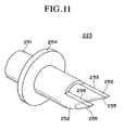
- Figure 11 is a perspective view showing the structure of the filter support member 223 included in the filter support component 220 in more detail.
- the filter support member 223 comprises a cylindrical portion 251, first and second projecting portions 252 and 253 provided on one end of the cylindrical portion 251, and a ring portion 254 provided on the peripheral of the cylindrical portion 251.
- the ring portion 254 functions as a stop for the filter support component 220 to the main housing 210.
- the first and second projecting portions 252 and 253 are curved parts formed by cutting a section of the end of the cylindrical portion 251 crossly and cutting another part the cylindrical portion 251.
- the first and second projecting portions 252 and 253 each has a surface (first surface) 255 that is at an angle of 45 degrees to the path of the transmitting light 100a.
- the first optical filter 261 is maintained on this first surface 255.
- the first and second projecting portions 252 and 253 also has a surface (second surface) 256 that is substantially perpendicular to the light-receiving component 140, and on which the second optical filter 262 is maintained.
- the first optical filter 261 reflects the receiving light 100b from the optical fiber 221 and transmits transmitting light 100a emitted by the light-emitting component 130.
- the second optical filter 162 transmits the receiving light 100b from the optical fiber 221 and reflects the transmitting light 100a from the light-emitting component 130. This makes it possible for the optical module 200 to function in the same way as the optical module 100.
Landscapes
- Physics & Mathematics (AREA)
- General Physics & Mathematics (AREA)
- Optics & Photonics (AREA)
- Optical Couplings Of Light Guides (AREA)
- Semiconductor Lasers (AREA)
- Light Receiving Elements (AREA)
Applications Claiming Priority (2)
| Application Number | Priority Date | Filing Date | Title |
|---|---|---|---|
| JP2004046528 | 2004-02-23 | ||
| JP2004046528A JP2005234464A (ja) | 2004-02-23 | 2004-02-23 | 光トランシーバ及びこれに用いる光モジュール |
Publications (1)
| Publication Number | Publication Date |
|---|---|
| EP1566675A1 true EP1566675A1 (de) | 2005-08-24 |
Family
ID=34709181
Family Applications (1)
| Application Number | Title | Priority Date | Filing Date |
|---|---|---|---|
| EP05251073A Withdrawn EP1566675A1 (de) | 2004-02-23 | 2005-02-23 | Optischer Sender-Empfänger und optisches Modul dafür |
Country Status (5)
| Country | Link |
|---|---|
| US (1) | US7048451B2 (de) |
| EP (1) | EP1566675A1 (de) |
| JP (1) | JP2005234464A (de) |
| CN (1) | CN1661407A (de) |
| TW (1) | TWI387793B (de) |
Families Citing this family (23)
| Publication number | Priority date | Publication date | Assignee | Title |
|---|---|---|---|---|
| JP2005197659A (ja) * | 2003-12-08 | 2005-07-21 | Sony Corp | 光学装置及び画像生成装置 |
| KR100640421B1 (ko) * | 2004-12-28 | 2006-10-31 | 삼성전자주식회사 | 다파장용 광소자 모듈 |
| CN2898856Y (zh) * | 2005-08-29 | 2007-05-09 | 昂纳信息技术(深圳)有限公司 | 一体化封装光电组件 |
| US20100028000A1 (en) * | 2005-12-16 | 2010-02-04 | Allen Ho | Module with both analog and digital receiving-transmitting |
| JP5144498B2 (ja) * | 2006-04-06 | 2013-02-13 | 日本電信電話株式会社 | 一心双方向光送受信モジュール及びその製造方法 |
| JP4943739B2 (ja) * | 2006-05-18 | 2012-05-30 | 浜松ホトニクス株式会社 | 光送受信デバイス |
| JP5125235B2 (ja) * | 2006-06-26 | 2013-01-23 | 住友電気工業株式会社 | 光送受信装置および光送受信モジュール |
| JP5139651B2 (ja) * | 2006-07-06 | 2013-02-06 | 富士通コンポーネント株式会社 | 光電変換モジュールの組み立て方法及び実装システム |
| JPWO2008139763A1 (ja) * | 2007-05-14 | 2010-07-29 | 株式会社フジクラ | 光通信モジュールとその製造方法及び光送受信装置 |
| TW200900771A (en) * | 2007-06-29 | 2009-01-01 | Delta Electronics Inc | Optomechanical structure and its optical transmitting element |
| US7743763B2 (en) * | 2007-07-27 | 2010-06-29 | The Boeing Company | Structurally isolated thermal interface |
| US8411451B2 (en) * | 2008-07-30 | 2013-04-02 | Panasonic Corporation | Power line communication apparatus |
| US7637672B1 (en) * | 2008-11-02 | 2009-12-29 | Broadway Networks, Ltd. | Pluggable optical tranceiver module having effective thermal release function |
| US8545112B2 (en) * | 2011-09-14 | 2013-10-01 | Ezconn Corporation | Main housing for optical sub-assembly for transceivers |
| KR101342097B1 (ko) * | 2011-10-26 | 2013-12-18 | 한국전자통신연구원 | 다채널 광모듈 |
| CN102570291B (zh) * | 2011-12-20 | 2014-10-08 | 西安炬光科技有限公司 | 一种传导制冷型高功率半导体激光器及其制备方法 |
| JP5942426B2 (ja) * | 2011-12-28 | 2016-06-29 | 日亜化学工業株式会社 | 光源装置 |
| KR101170937B1 (ko) | 2012-03-29 | 2012-08-03 | (주)에이알텍 | 광통신용 광모듈 |
| KR101755966B1 (ko) * | 2013-02-28 | 2017-07-07 | 미쓰비시덴키 가부시키가이샤 | 방열 구조 및 광 송수신기 |
| JP6494094B2 (ja) * | 2015-03-09 | 2019-04-03 | 住友電工デバイス・イノベーション株式会社 | 光モジュール |
| US20190113698A1 (en) * | 2017-10-18 | 2019-04-18 | Source Photonics, Inc. | Integrated Heat Sink and Optical Transceiver Including the Same |
| JP7500959B2 (ja) * | 2019-12-10 | 2024-06-18 | 住友電気工業株式会社 | 光トランシーバ |
| JP7452774B1 (ja) * | 2023-10-30 | 2024-03-19 | 三菱電機株式会社 | 光半導体装置および光トランシーバ |
Citations (3)
| Publication number | Priority date | Publication date | Assignee | Title |
|---|---|---|---|---|
| EP0331436A2 (de) * | 1988-03-01 | 1989-09-06 | Kabushiki Kaisha Toshiba | Optische Übertragungsvorrichtung |
| US6332720B1 (en) * | 1998-09-17 | 2001-12-25 | Hitachi, Ltd. | Semiconductor laser coupling device and method for assembling the same on circuit board |
| US20020028049A1 (en) * | 2000-09-05 | 2002-03-07 | Meir Bartur | Optical networking unit employing optimized optical packaging |
Family Cites Families (32)
| Publication number | Priority date | Publication date | Assignee | Title |
|---|---|---|---|---|
| US4210704A (en) * | 1978-08-04 | 1980-07-01 | Bell Telephone Laboratories, Incorporated | Electrical devices employing a conductive epoxy resin formulation as a bonding medium |
| JPS58219259A (ja) * | 1982-06-14 | 1983-12-20 | Toray Silicone Co Ltd | 熱伝導性シリコ−ンゴム組成物 |
| US4595606A (en) * | 1984-07-18 | 1986-06-17 | Rohm And Haas Company | Solderable conductive compositions having high adhesive strength |
| JPS61156208A (ja) | 1984-12-28 | 1986-07-15 | Fujitsu Ltd | 波長選択素子及び波長選択器 |
| US4904043A (en) * | 1988-06-15 | 1990-02-27 | American Telephone And Telegraph Company, At&T Bell Laboratories | Optical data link dual wavelength coupler |
| JPH0619027B2 (ja) * | 1989-02-13 | 1994-03-16 | 信越化学工業株式会社 | 熱伝導性シリコーンオイルコンパウンド |
| US5060114A (en) * | 1990-06-06 | 1991-10-22 | Zenith Electronics Corporation | Conformable pad with thermally conductive additive for heat dissipation |
| DE4136893A1 (de) | 1991-11-09 | 1993-05-13 | Ant Nachrichtentech | Optische sende- und empfangsanordnung |
| JP3095902B2 (ja) | 1992-08-26 | 2000-10-10 | イビデン株式会社 | カルボキシル基を導入した光ファイバーの製造方法 |
| DE59310297D1 (de) | 1993-09-15 | 2002-09-05 | Infineon Technologies Ag | Sende- und Empfangsmodul für eine bidirektionale optische Mehrkanal-Übertragung |
| US5487124A (en) * | 1994-06-30 | 1996-01-23 | The Whitaker Corporation | Bidirectional wavelength division multiplex transceiver module |
| EP0706069B1 (de) | 1994-10-06 | 2003-04-02 | Infineon Technologies AG | Sende- und Empfangsmodul für eine bidirektionale optische Nachrichten- und Signalübertragung |
| CA2161718A1 (en) * | 1994-10-31 | 1996-05-01 | Hiromi Kurashima | Optical module having structure for defining fixing position of sleeve |
| JP3334381B2 (ja) | 1994-12-02 | 2002-10-15 | 三菱電機株式会社 | 光半導体素子モジュール |
| US5661835A (en) * | 1995-01-19 | 1997-08-26 | Sumitomo Electric Industries, Ltd. | Optical composite module and method of assembling the same |
| JP3142800B2 (ja) * | 1996-08-09 | 2001-03-07 | 信越化学工業株式会社 | 熱伝導性シリコーン組成物、熱伝導性材料及び熱伝導性シリコーングリース |
| US6071016A (en) * | 1997-03-04 | 2000-06-06 | Hamamatsu Photonics K.K. | Light receiving module for optical communication and light receiving unit thereof |
| EP1082632A1 (de) | 1998-04-30 | 2001-03-14 | Siemens Aktiengesellschaft | Bidirektionales optisches modul für mehrkanal-anwendung |
| JP4121185B2 (ja) * | 1998-06-12 | 2008-07-23 | 新電元工業株式会社 | 電子回路装置 |
| US6356686B1 (en) * | 1999-09-03 | 2002-03-12 | International Business Machines Corporation | Optoelectronic device encapsulant |
| US6508595B1 (en) * | 2000-05-11 | 2003-01-21 | International Business Machines Corporation | Assembly of opto-electronic module with improved heat sink |
| GB2373374B (en) | 2001-03-15 | 2004-03-17 | Agilent Technologies Inc | Novel fiber optic transceiver module |
| JP4703022B2 (ja) | 2001-03-29 | 2011-06-15 | 京セラ株式会社 | 送受信モジュール |
| JP4841079B2 (ja) | 2001-08-30 | 2011-12-21 | 京セラ株式会社 | 光デバイス |
| US20030053768A1 (en) | 2001-09-20 | 2003-03-20 | International Business Machines Corporation | Fiber optic transceiver, connector, and method of dissipating heat |
| US6571033B2 (en) | 2001-09-28 | 2003-05-27 | Corning Incorporated | Optical signal device |
| US6893167B1 (en) * | 2002-01-17 | 2005-05-17 | Opnext, Inc. | Mountable optical transceiver |
| US6788540B2 (en) | 2002-01-30 | 2004-09-07 | Jds Uniphase Corporation | Optical transceiver cage |
| JP2003255196A (ja) | 2002-02-27 | 2003-09-10 | Kyocera Corp | 光モジュール及びその組立方法 |
| US6916122B2 (en) * | 2002-03-05 | 2005-07-12 | Jds Uniphase Corporation | Modular heat sinks |
| EP1343038A1 (de) * | 2002-03-09 | 2003-09-10 | Agilent Technologies, Inc. - a Delaware corporation - | Unter Spannung steckbares opto-elektronisches Modul mit Dichtung zur elektromagnetischen Abschirmung |
| JP2004085971A (ja) * | 2002-08-28 | 2004-03-18 | Opnext Japan Inc | 光伝送モジュール |
-
2004
- 2004-02-23 JP JP2004046528A patent/JP2005234464A/ja active Pending
- 2004-07-07 US US10/885,032 patent/US7048451B2/en not_active Expired - Fee Related
- 2004-11-25 CN CN2004100962084A patent/CN1661407A/zh active Pending
-
2005
- 2005-01-17 TW TW094101279A patent/TWI387793B/zh not_active IP Right Cessation
- 2005-02-23 EP EP05251073A patent/EP1566675A1/de not_active Withdrawn
Patent Citations (3)
| Publication number | Priority date | Publication date | Assignee | Title |
|---|---|---|---|---|
| EP0331436A2 (de) * | 1988-03-01 | 1989-09-06 | Kabushiki Kaisha Toshiba | Optische Übertragungsvorrichtung |
| US6332720B1 (en) * | 1998-09-17 | 2001-12-25 | Hitachi, Ltd. | Semiconductor laser coupling device and method for assembling the same on circuit board |
| US20020028049A1 (en) * | 2000-09-05 | 2002-03-07 | Meir Bartur | Optical networking unit employing optimized optical packaging |
Also Published As
| Publication number | Publication date |
|---|---|
| US7048451B2 (en) | 2006-05-23 |
| TW200530644A (en) | 2005-09-16 |
| CN1661407A (zh) | 2005-08-31 |
| US20050185899A1 (en) | 2005-08-25 |
| JP2005234464A (ja) | 2005-09-02 |
| TWI387793B (zh) | 2013-03-01 |
Similar Documents
| Publication | Publication Date | Title |
|---|---|---|
| US7048451B2 (en) | Optical transceiver and optical module used in the same | |
| US20070114547A1 (en) | Optical element sealing structure, optical coupler, and optical element sealing method | |
| JP3861864B2 (ja) | 光モジュール | |
| CN100428507C (zh) | 光发送器 | |
| US7290942B2 (en) | Optical transceiver modules | |
| CN102422193B (zh) | 具有陶瓷封装的光学装置的光学组件 | |
| CN110708122A (zh) | 高导热收发一体光模块 | |
| EP3121630A1 (de) | Optoelektronisches modul mit verbesserter wärmeverwaltung | |
| KR20010070487A (ko) | 광섬유 접속부 및 그것의 사용 방법 | |
| CN1846466A (zh) | 具有陶瓷馈通头部组件的发射器光学子组件中的激光监视和控制 | |
| CN1981390A (zh) | 发光二极管装置 | |
| KR20180042600A (ko) | 광학모듈 | |
| JP3982561B2 (ja) | Led照明装置 | |
| EP1557704A2 (de) | Kühlkörperelement für optische Baugruppe und Zusammenbauverfahren | |
| EP1555555A1 (de) | Optisches Modul für bi-direktionales Kommunikationssystem | |
| US6634803B2 (en) | External EMI shield for multiple array optoelectronic devices | |
| CA2449884A1 (en) | Powerpack laser diode assemblies | |
| US20030002825A1 (en) | Carrier sub-assembly with inserts and method for making the same | |
| EP1555554A1 (de) | Optisches Modul für ein bidirektionales Kommunikationssystem | |
| US6666589B2 (en) | Internal EMI shield for multiple array optoelectronic devices | |
| US20030086660A1 (en) | Horizontal carrier assembly for multiple array optoelectronic devices | |
| US6430326B1 (en) | Module for parallel optical data transmission | |
| JPH10247741A (ja) | 光通信用発光モジュールおよびその組立方法 | |
| US7073958B2 (en) | Optical module | |
| JP3420406B2 (ja) | 光通信用モジュール |
Legal Events
| Date | Code | Title | Description |
|---|---|---|---|
| PUAI | Public reference made under article 153(3) epc to a published international application that has entered the european phase |
Free format text: ORIGINAL CODE: 0009012 |
|
| AK | Designated contracting states |
Kind code of ref document: A1 Designated state(s): AT BE BG CH CY CZ DE DK EE ES FI FR GB GR HU IE IS IT LI LT LU MC NL PL PT RO SE SI SK TR |
|
| AX | Request for extension of the european patent |
Extension state: AL BA HR LV MK YU |
|
| AKX | Designation fees paid |
Designated state(s): AT BE BG CH CY CZ DE DK EE ES FI FR GB GR HU IE IS IT LI LT LU MC NL PL PT RO SE SI SK TR |
|
| STAA | Information on the status of an ep patent application or granted ep patent |
Free format text: STATUS: THE APPLICATION IS DEEMED TO BE WITHDRAWN |
|
| 18D | Application deemed to be withdrawn |
Effective date: 20060425 |