EP1564794B1 - Verfahren und vorrichtung zur erzeugung von gleichmaessigem hochfrequenzplasma über einen grossen oberflaechenbereich - Google Patents
Verfahren und vorrichtung zur erzeugung von gleichmaessigem hochfrequenzplasma über einen grossen oberflaechenbereich Download PDFInfo
- Publication number
- EP1564794B1 EP1564794B1 EP02777987A EP02777987A EP1564794B1 EP 1564794 B1 EP1564794 B1 EP 1564794B1 EP 02777987 A EP02777987 A EP 02777987A EP 02777987 A EP02777987 A EP 02777987A EP 1564794 B1 EP1564794 B1 EP 1564794B1
- Authority
- EP
- European Patent Office
- Prior art keywords
- plasma
- high frequency
- power supply
- surface area
- large surface
- Prior art date
- Legal status (The legal status is an assumption and is not a legal conclusion. Google has not performed a legal analysis and makes no representation as to the accuracy of the status listed.)
- Expired - Lifetime
Links
- 238000000034 method Methods 0.000 title claims description 25
- 238000005229 chemical vapour deposition Methods 0.000 claims description 55
- 238000004140 cleaning Methods 0.000 claims description 18
- 230000010363 phase shift Effects 0.000 claims description 11
- 230000010355 oscillation Effects 0.000 claims description 6
- 239000000203 mixture Substances 0.000 claims description 3
- 210000002381 plasma Anatomy 0.000 description 145
- 239000007789 gas Substances 0.000 description 61
- 239000010408 film Substances 0.000 description 33
- 239000000758 substrate Substances 0.000 description 24
- 229910021417 amorphous silicon Inorganic materials 0.000 description 16
- 238000009826 distribution Methods 0.000 description 10
- 238000010438 heat treatment Methods 0.000 description 10
- 239000010409 thin film Substances 0.000 description 9
- BLRPTPMANUNPDV-UHFFFAOYSA-N Silane Chemical compound [SiH4] BLRPTPMANUNPDV-UHFFFAOYSA-N 0.000 description 8
- 238000010586 diagram Methods 0.000 description 8
- 229910000077 silane Inorganic materials 0.000 description 8
- XUIMIQQOPSSXEZ-UHFFFAOYSA-N Silicon Chemical compound [Si] XUIMIQQOPSSXEZ-UHFFFAOYSA-N 0.000 description 7
- 238000005516 engineering process Methods 0.000 description 7
- 229910052710 silicon Inorganic materials 0.000 description 7
- 239000010703 silicon Substances 0.000 description 7
- 239000004065 semiconductor Substances 0.000 description 6
- 239000013081 microcrystal Substances 0.000 description 4
- 229910052581 Si3N4 Inorganic materials 0.000 description 3
- 210000004027 cell Anatomy 0.000 description 3
- 230000000694 effects Effects 0.000 description 3
- HQVNEWCFYHHQES-UHFFFAOYSA-N silicon nitride Chemical compound N12[Si]34N5[Si]62N3[Si]51N64 HQVNEWCFYHHQES-UHFFFAOYSA-N 0.000 description 3
- 230000015572 biosynthetic process Effects 0.000 description 2
- 238000000151 deposition Methods 0.000 description 2
- 238000005530 etching Methods 0.000 description 2
- 238000004519 manufacturing process Methods 0.000 description 2
- 239000002994 raw material Substances 0.000 description 2
- 239000012495 reaction gas Substances 0.000 description 2
- 238000012935 Averaging Methods 0.000 description 1
- YCKRFDGAMUMZLT-UHFFFAOYSA-N Fluorine atom Chemical compound [F] YCKRFDGAMUMZLT-UHFFFAOYSA-N 0.000 description 1
- 239000003990 capacitor Substances 0.000 description 1
- 230000002508 compound effect Effects 0.000 description 1
- 238000002425 crystallisation Methods 0.000 description 1
- 230000008025 crystallization Effects 0.000 description 1
- 230000001186 cumulative effect Effects 0.000 description 1
- 230000007423 decrease Effects 0.000 description 1
- 230000007547 defect Effects 0.000 description 1
- 230000008021 deposition Effects 0.000 description 1
- 229910052731 fluorine Inorganic materials 0.000 description 1
- 239000011737 fluorine Substances 0.000 description 1
- 150000002500 ions Chemical class 0.000 description 1
- 239000000463 material Substances 0.000 description 1
- 238000009828 non-uniform distribution Methods 0.000 description 1
- 239000000376 reactant Substances 0.000 description 1
- 238000004904 shortening Methods 0.000 description 1
- 239000007787 solid Substances 0.000 description 1
Images




Classifications
-
- H—ELECTRICITY
- H01—ELECTRIC ELEMENTS
- H01J—ELECTRIC DISCHARGE TUBES OR DISCHARGE LAMPS
- H01J37/00—Discharge tubes with provision for introducing objects or material to be exposed to the discharge, e.g. for the purpose of examination or processing thereof
- H01J37/32—Gas-filled discharge tubes
- H01J37/32009—Arrangements for generation of plasma specially adapted for examination or treatment of objects, e.g. plasma sources
- H01J37/32082—Radio frequency generated discharge
- H01J37/32174—Circuits specially adapted for controlling the RF discharge
-
- C—CHEMISTRY; METALLURGY
- C23—COATING METALLIC MATERIAL; COATING MATERIAL WITH METALLIC MATERIAL; CHEMICAL SURFACE TREATMENT; DIFFUSION TREATMENT OF METALLIC MATERIAL; COATING BY VACUUM EVAPORATION, BY SPUTTERING, BY ION IMPLANTATION OR BY CHEMICAL VAPOUR DEPOSITION, IN GENERAL; INHIBITING CORROSION OF METALLIC MATERIAL OR INCRUSTATION IN GENERAL
- C23C—COATING METALLIC MATERIAL; COATING MATERIAL WITH METALLIC MATERIAL; SURFACE TREATMENT OF METALLIC MATERIAL BY DIFFUSION INTO THE SURFACE, BY CHEMICAL CONVERSION OR SUBSTITUTION; COATING BY VACUUM EVAPORATION, BY SPUTTERING, BY ION IMPLANTATION OR BY CHEMICAL VAPOUR DEPOSITION, IN GENERAL
- C23C16/00—Chemical coating by decomposition of gaseous compounds, without leaving reaction products of surface material in the coating, i.e. chemical vapour deposition [CVD] processes
- C23C16/44—Chemical coating by decomposition of gaseous compounds, without leaving reaction products of surface material in the coating, i.e. chemical vapour deposition [CVD] processes characterised by the method of coating
- C23C16/50—Chemical coating by decomposition of gaseous compounds, without leaving reaction products of surface material in the coating, i.e. chemical vapour deposition [CVD] processes characterised by the method of coating using electric discharges
- C23C16/505—Chemical coating by decomposition of gaseous compounds, without leaving reaction products of surface material in the coating, i.e. chemical vapour deposition [CVD] processes characterised by the method of coating using electric discharges using radio frequency discharges
- C23C16/509—Chemical coating by decomposition of gaseous compounds, without leaving reaction products of surface material in the coating, i.e. chemical vapour deposition [CVD] processes characterised by the method of coating using electric discharges using radio frequency discharges using internal electrodes
-
- H—ELECTRICITY
- H01—ELECTRIC ELEMENTS
- H01J—ELECTRIC DISCHARGE TUBES OR DISCHARGE LAMPS
- H01J37/00—Discharge tubes with provision for introducing objects or material to be exposed to the discharge, e.g. for the purpose of examination or processing thereof
- H01J37/32—Gas-filled discharge tubes
- H01J37/32009—Arrangements for generation of plasma specially adapted for examination or treatment of objects, e.g. plasma sources
- H01J37/32082—Radio frequency generated discharge
Definitions
- the present invention relates to a method and device for generating uniform high-frequency plasma over a large surface area used for a plasma chemical vapor deposition apparatus.
- the plasma chemical vapor deposition apparatus is used for forming or etching the semiconductor films from amorphous silicon, microcrystal silicon, multicrystal thin films silicon, silicon nitride, etc. for use in solar cells, thin film transistors or the like, and used for performing fluorine radical cleaning (self-cleaning) which cleans the amorphous silicon (a-Si) deposits inside the film-forming chamber using NF 3 gas plasma.
- a high frequency plasma generator device used in a plasma chemical vapor deposition apparatus performs forming or etching the semiconductor films from amorphous silicon (hereinafter abbreviated "a-Si"), microcrystal silicon, multicrystal thin films silicon, silicon nitride, etc. for use in solar cells, thin film transistors or the like, and performs self-cleaning for the silicon deposits in the film forming chamber using NF 3 gas.
- the high frequency plasma generator device may employ one of two types of electrodes: a parallel flat plate type electrode or a ladder type electrode.
- FIG. 6 illustrates an example of a device employing the parallel flat plate type electrode.
- Substrate heating support means 6 is installed inside of the plasma chemical vapor deposition apparatus 1 and contacts to the ground electrically.
- Flat plate electrode 60 is separated, for example, by 20 mm from the opposing substrate heating support means 6.
- the flat plate electrode 60 is connected to an external high frequency power source 61 via an impedance matching controller 62 and coaxial cable 63.
- ground seal 5 prevents the generation of unwanted plasma on the side opposite from the side facing the substrate heating support means 6.
- substrate 7 for the a-Si film forming is placed atop the substrate heating support means 6 at a set temperature, for example, of 200°C; silane gas (SiH 4 ) is introduced via the gas inlet pipe 64 at a flow velocity, for example, of 50 sccm; and a vacuum pump (not shown) connected to vacuum exhaust pipe 65 is operated to adjust the exhaust flow rate, and resultingly, the inside pressure in the plasma chemical vapor deposition apparatus 1 is set, for example, to 100 mTorr.
- the plasma 66 is generated between substrate 7 and the flat plate electrode 60 by supplying high frequency power from the high frequency power source 61, which is adjusted by the impedance matching controller 62, to create highly efficient plasma generation in the plasma generator device.
- the SiH 4 breaks down and an a-Si film is formed on the surface of the substrate 7. An adequate thickness of a-Si film may be deposited in this manner over the course of approximately 10 minutes.
- FIG. 7 An example of a ladder type of high frequency plasma generator device structure is shown in Figure 7;
- Figure 8 shows a diagram from the A-direction in Figure 7 to further elucidate the structure of the ladder-type electrode 70.
- the structure of such ladder-type electrodes 70 is described in detail in Japanese Patent Publication Hei 4-236781 , etc., while Japanese Patent Publication Hei 11-111622 discloses an evolved form of the ladder-type electrode in which a plurality of parallel electrode rods are arrayed into an electrode group, and where two such groups are arrayed orthogonally to form an electrode mesh.
- substrate heating support means 6 (not shown in Figure 8 )is electrically connected to the ground, which is provided inside of the plasma chemical vapor deposition apparatus, and ladder-type electrode 70 is positioned opposite to the substrate heating support means 6 at a distance, for example, of 20 mm.
- the ladder-type electrode 70 is electrically connected to an external high frequency power source 61 via impedance matching controller 62 and coaxial cable 63.
- Ground shield 5 is positioned to prevent unwanted plasma from being generated on the side opposite the surface facing substrate heating support means 6.
- substrate 7 for the a-Si film forming is placed atop the substrate heating support means 6 at a set temperature, for example, of 200°C, and silane gas (SiH 4 ) is introduced via the gas inlet pipe at a flow velocity, for example, of 50 sccm.
- a vacuum pump (not shown) connected to vacuum exhaust pipe is operated to adjust the exhaust flow rate, and resultingly, the inside pressure in the plasma chemical vapor deposition apparatus 1 is set, for example, to 100 mTorr. Since the plasma 71 is generated between substrate 7 and the ladder-type electrode 70 by supplying high frequency power to the ladder-type electrode 70, the impedance matching controller 62 can be adjusted to create highly efficient plasma generation in the plasma generator device. Inside of plasma 71, then, the silane (SiH 4 ) breaks down and an a-Si film is formed on the surface of the substrate 7. Thus an adequate thickness of a-Si film may be deposited in this manner over the course of approximately 10 minutes.
- Such plasma chemical vapor deposition apparatus include a high frequency plasma generator device, but there is an ongoing demand for devices that can fabricate thin film semiconductors for solar cells, thin film transistors for flat panel displays and the like, in low cost by manufacturing a large surface area (e.g. approximately 1.5 x 1.2 m) at high speed, and in high quality by lowering the defect density and achieving the high level crystallization rate. Additionally, a demand exists for high speed, large surface area self-cleaning using NF 3 gas of the a-Si deposits that accumulate in the chambers where the large surface area film forming takes place, which is the same demand for fabricating thin films.
- NF 3 gas of the a-Si deposits that accumulate in the chambers where the large surface area film forming takes place, which is the same demand for fabricating thin films.
- the NF 3 plasma used in self-cleaning being a negatively charged gas (electrons adhere easily), causes the plasma itself to be very unstable, and in addition its distribution is nonuniform due to the gas flow (the plasma being generated on the downstream side) and differences in the distance between electrodes.
- the electrode size exceeds 30 cm x 30 cm.
- the frequency exceeds 30 MHz, the above described effects become pronounced and it is difficult to achieve even the minimal uniformity in film thickness of ⁇ 10% for manufacturing the semiconductor film.
- the objective of that technology was to control the volume of active ions and other inflow as well as the irradiated energy by means of using the one high frequency wave for plasma generation and the other to control the bias voltage on the surface of the dielectric substrate. That objective differs completely from the objective of the present invention of producing uniform plasma generation over an exceeding large substrate of 1 m x 1 m.
- the present invention was developed to resolve the aforementioned problems and has as its objective, the provision of a uniformization method and device for high frequency plasma over large surface areas, by employing a plasma chemical vapor deposition apparatus that generates uniform plasma over a large surface area using a very high frequency (VHF) plasma chemical vapor deposition apparatus.
- VHF very high frequency
- US2001/0021422A1 discloses a discharge plasma generating method, comprising applying HF-power to discharge electrodes so that an envelope representing the spatial distribution of a HF voltage on a discharge electrode changes in accordance with a function including time as a parameter.
- this document discloses a plasma generation method for generating high frequency plasma uniformly over a large surface area in a plasma chemical vapor deposition apparatus in which the plasma is generated by supplying high frequency power to a discharge electrode, comprising the steps of: applying high frequency (of 60.3 MHz) power supply to a first power supply section while applying high frequency power supply to a second power supply section with a different frequency (of 59.8 MHz).
- the present invention installs a first and a second power supply section on both ends of the discharge electrode, which are supplied with alternate cycles: the first cycle wherein the first and second power supply sections receive high frequency waves at the same frequency, and a second cycle wherein different high frequency waves are received, whereby the standing waves generated in each cycle form in different positions during the plasma generation, which, when averaged over time, makes possible uniform plasma generation over a large surface area.
- the present invention relates a plasma generation method according to claim 1.
- the present invention provides a device according to claim 12.
- the waves coming from both sides resonate in the middle to increase the plasma density in that area, but on the other hand, when the waves from both sides of the electrode are of different frequencies, they tend to cancel each other out at the center to lower the plasma density in that area.
- the generation of the plasma is such that the standing wave distribution is uniform over the large surface area above the discharge electrode, which results in a uniform thickness of deposition on the large surface area substrate, as well as uniform self-cleaning.
- a preferred implementation of the foregoing method of this invention is to vary one of the frequencies in the second cycle over time to intentionally vary the state of the plasma generation in a manner such that, when viewed as an average over time, the plasma is generated uniformly over the large surface area, and further, the second oscillator has a variable oscillation frequency.
- the state of plasma generation may be varied accordingly to further average the plasma density.
- one of the frequencies used during the cycle using different frequencies, particularly one of frequencies in the second cycle may be the same frequency as the frequency in the first cycle.
- the switching to alternate between the first and second cycles may fall within the range of 1 time/second to 10 million times/second.
- the time ratio between the first cycle and the second cycle may be varied, depending on the gas pressure and the type of gas being used.
- time ratio between the first cycle and the second cycle may be varied, depending on the pressure and the type of the gas being used, and the time ratio between the first and second frequencies that are switched by the switching means may also be varied and set to an appropriate value depending upon the gas pressure and the type of gas based upon inputs into the function generator.
- the time ratio between the first cycle and second cycle may be varied according to the gas pressure and type of gas; for example, using an identical duty cycle, different gas conditions could cause the state of plasma generation to differ. However, such a situation could be handled and a uniform plasma density could be achieved in this manner without requiring any hardware changes.
- phase shift modulation may be applied to the high frequency waves supplied to the first or second power supply section during the first cycle to vary the state of plasma generation by shifting the phase from the other high frequency to produce uniform plasma generation over a large surface area when averaged over time.
- phase shift modulation means which is incorporated to modulate the phase of the high frequency waves supplied from the first oscillator to the high frequency power source A or the frequency switching means.
- the phase of the high frequency waves may be shifted toward the other side to make possible, using a single frequency application to the discharge electrode, to shift the high density plasma off the center and thereby make the plasma uniform when averaged over time.
- a direct current bias may be applied to the power supply section of the discharge electrode in order to uniformize the generated plasma density over a large surface area.
- this involves the addition of a means to apply a direct current bias to the power supply section of the discharge electrode.
- the application of the direct current bias to the power supply section of the discharge electrode makes it possible to reduce the sheath capacitance of the discharge electrode, which increases the wavelength of the standing wave to uniformize the plasma density.
- an axial direction of power supply cables to the first and second power supply sections may be matched to the axial direction of the di scharge electrode to minimize the current return distances, and reduce the power loss from the power source, to thereby increase range over which the plasma is generated.
- the power supply cable to the power supply section of the discharge electrode should be connected in a manner such that the axial direction of the cable matches the axial direction of the discharge electrode.
- the power from the power source can smoothly enter the discharge electrode, and the minimization of the current return distance reduces the power losses to increase the range over which plasma is generated.
- the present invention is characterized by the configuration, in which gas may be delivered that readily forms plasma to the inside of the plasma chemical vapor deposition apparatus being within a range to satisfy the conditions required for rapid film forming by plasma chemical vapor deposition and rapid self-cleaning of the plasma chemical vapor deposition apparatus.
- gas mixtures that contain inactive gasses such as N 2 , Ar, Kr, Xe or combinations thereof.
- the basic configuration of this invention provides for a plasma chemical vapor deposition apparatus of the class that can accommodate an electrode size of 1.5 m x 1.2 m, a gas pressure of 12 to 20 Pa (90-150 mTorr) while utilizing a high frequency power source of 60 MHz.
- a first and a second power supply section are established on each end of the discharge electrode in the plasma chemical vapor deposition apparatus; these are powered alternately with high frequency waves in two cycles, a cycle in which the same frequency of high frequency is supplied, and a cycle in which different frequencies of high frequency power are supplied.
- the plasma generation in other words, the standing wave distribution over the discharge electrode, is uniform over the large surface area by the different plasma generation in each cycle. Further, in this present invention, the following six ways can be used to uniformize time-averaged plasma generation to thereby make it possible to work with exceedingly large substrate targets exceeding 1 m x 1 m in size.
- Figure 1 is a block diagram depicting an embodiment of the plasma generation device for generating high frequency plasma uniformly over a large surface area in the plasma chemical vapor deposition apparatus of this invention.
- Figure 2 is a diagram used to explain a ladder-type structure for the discharge electrode.
- Figure 3 is a diagram showing the power source cable outlet in the axial direction and the aligning of the first and second power supply section connection to match (in the axial direction).
- Figure 4 is a graph showing the plasma generation state using 10 types of cycle ratios that range from 0 : 10 to 9 : 1, for the supply of the same frequency of high frequency waves and a different frequency of high frequency waves to the power supply section of the discharge electrode.
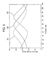
- Figure 5 is a graph showing the phase shift of the one high frequency wave with respect to the other when the same frequency of high frequency power is supplied to the power supply sections.
- 1 represents a plasma chemical vapor deposition apparatus having an air-tight interior
- 2 is the discharge electrode
- 3, 4 are the first and second power supply sections for the supply of power to discharge electrode 2
- 5 is a ground shield to prevent unwanted plasma formation
- 6 is the substrate heating support means which is located, for example, at 20 to 34 mm distance from discharge electrode 2, and which contains an internal heater and mechanism not shown in the figure
- 8 is a gas inlet pipe connected to a gas supply source (not shown), which, for example, allows the introduction of reactive gasses 9 such as silane (SiH 4 ) gas for film forming and NF 3 for self-cleaning
- 10 is a gas exhaust pipe
- 11 is a vacuum pump, which enables the internal pressure of the plasma chemical vapor deposition apparatus 1 to be reduced to approximately 1 x 10 -6 Torr
- 12 and 13 are RF amplifiers comprising the first and second high frequency power sources A and B
- 14 is a first high frequency (RF) oscillator, which incorporates a phase shifter, to
- the first high frequency oscillator 14 oscillates, as previously stated, for example, at 60 MHz, and that signal is sent to the high frequency power source A 12 or the switch 16, while the second high frequency oscillator 15, oscillates, for example, at 58.5 MHz and is switched at switch 16.
- This switch 16 switches the 60 MHz signal sent from the first high frequency oscillator 14 and the 58.5 MHz sent from the second high frequency oscillator 15 in a constant cycle and sends the high frequency to the high frequency power source B 13.
- the high frequency power source A 12 supplies the 60MHz high frequency to the first power supply section 3, while the high frequency power source B 13 supplies the 60 MHz and the 58.5 MHz radio frequencies switched at constant cycles to the second power supply section 4.
- the switch 16 which switches the 60 MHz from the first high frequency oscillator 14, and the 58.5 MHz from the second high frequency oscillator 15, is such that it can switch at a variable time ratio, in other words, a variable duty cycle based upon a signal from function generator 17 that reflects the gas conditions such as type of gas, pressure, etc.
- the first high frequency oscillator 14 incorporates an internal phase shifter which makes possible the phase shifting of the one high frequency with respect to the other frequency that is fed to either high frequency power source A 12 or switch 16.
- the second high frequency oscillator 15 has a variable configuration to enable it to oscillate, for example, from 58.5 MHz to 59.9MHz or from 60.1 MHz to 61.5 MHz.
- the discharge electrode 2 of plasma chemical vapor deposition apparatus 1 is of the ladder type shown in Figure 2 , and as is shown in the Figure, the first power supply section 3 and the second power supply section 4 are established at 8 points each as shown by the black dots on both ends of discharge electrode 2.
- Power supply sections 3 and 4 of discharge electrode 2 have connections, 21 and 22 shown in Figure 3 for each ladder type electrode rungs 20, which are positioned in the same direction (axial direction) as the power supply sections 3, 4.
- a DC bias can be applied to discharge electrode 2 (20) from DC bias power source 23.
- discharge electrode 2 was of the ladder type, and power supply sections 3, 4 were located at 8 points each, but the present invention is not confined to ladder type discharge electrodes, it may also be applied to flat plate electrodes. Additionally, the connections are not confined to 8 points, there may be 4 points, 16 points, or other number as required by the application.
- power cables 21, 22 are coaxial cables or other appropriate types, such as parallel flat cable, or parallel wire cable.
- Sheath capacitance refers to the phenomena, in which a surrounding group of electrons (called a "sheath") is formed around a ladder type electrode 20 in the course of plasma generation, and the sheath maintaining a sort of dielectric state prevents direct currents from flowing in a manner similar to the state a capacitor exists around the electrode.
- the application of a negative DC bias scatters these electrons to thereby reduce the sheath capacitance. This increases the interval between the standing wave wavelengths and serves to make the plasma more uniform.
- substrate 7 When employing such a plasma chemical vapor deposition apparatus 1 configured according to this invention to create semiconductor films of a-Si, microcrystal silicon, multicrystal thin film silicon, silicon nitride, etc., or to perform self-cleaning of accumulated a-Si using NF 3 gas, during film forming, for example, substrate 7 would be affixed to substrate heating support means 6 which is set at 200°C while reaction gas 9, such as silane gas (SiH 4 ), would be introduced through gas inlet pipe 8 at a rate, for example, of 50 sccm, with vacuum pump 11 being connected to exhaust pipe 10 to adjust the exhaust flow rate to keep the pressure inside of the plasma chemical vapor deposition apparatus at, for example, 100 mTorr.
- reaction gas 9 such as silane gas (SiH 4 )
- the 60 MHz high frequency from the first high frequency oscillator 14, and the 58.5 MHz high frequency from the second high frequency oscillator 15 are respectively supplied to high frequency power source A 12 and switch 16.
- the operation of switch 16 switches the 60 MHz sent from the first high frequency oscillator 14 and the 58.5 MHz sent from the second high frequency oscillator 15 at a constant cycle and sends the high frequency to the high frequency power source B 13.
- the high frequency power source A 12 supplies 60 MHz high frequency to the first power supply section 3, while high frequency power source B 13 supplies the 60 MHz and 58.5 MHz radio frequencies that are switch at a constant cycle to the second power supply section 4.
- Figure 4 illustrates the differences in plasma states from the case where the 60 MHz very high frequency is supplied simultaneously to power supply sections 3, 4, and the case where the 60 MHz high frequency is supplied to the first power source section 3 while 58.5 MHz, a different high frequency, is supplied to the second power supply section 4.
- the graph in Figure 4 shows the case when silane (SiH 4 ) or other reactant gas 9 is introduced into the foregoing plasma chemical vapor deposition apparatus 1, and the same high frequency (60 MHz) is supplied to the first and second power supply sections 3, 4 of discharge electrode 2, and the case when differing frequencies are supplied (60 MHz to the first power supply section 3 and 58.5 MHz to the second power supply section 4) for 10 sets of conditions with the time ratio being varied from 0 : 10 to 9 : 1.
- the horizontal axis indicates the distance from the first power supply section 3 from (0 cm) to (110 cm) on the right, which corresponds to the distance to the second power supply section 4.
- the vertical axis shows the relative voltage value for the plasma. The higher this value the more dense the plasma.
- the a-curve shows the plasma generation state for the case when the supply time ratio for the different radio frequencies was 10 and that for the same radio frequencies was 0, in other words for the case where different frequencies were used all the time, while the b-curve shows the case for the supply time ratio of the different radio frequencies being 9 and the same frequency being 1. Thereafter, the case is similar for the n-curve, where the time ratio at the different frequencies was 1 and the same frequencies was 9.
- the graph of Figure 4 shows that when the same 60 MHz very high frequency is supplied to both power supply sections 3, 4 of discharge electrode 2, plasma density is higher at the center of the electrode, but when different frequencies are supplied, plasma density is lower at the center of the electrode.
- the present invention further provides a method for varying the oscillation frequency of the second high frequency oscillator 15 over time from 58.5 MHz to 59.9 MHz or 60.1 MHz to 61.5 MHz. Deliberately varying the frequency in this manner can be used to control the state of plasma generation to obtain an averaged plasma density over time.
- the inclusion of a phase shifter in the first high frequency oscillator 14, makes it possible to shift the phase of the high frequency sent to either high frequency power source A 12 or switch 16 with respect to the phase of the other high frequency.
- the power source is such that the plasma density is highest in the center of discharge electrode 2 when the phase is not shifted, but when the phase is shifted, the position of the high plasma density can be shifted to the areas shown by the broken lines 51, 52, to the left and right. Accordingly, when viewed over time, the plasma density is uniform over a broad area.
- function generator 17 to send the high frequency to switch 16 based upon gas conditions such as gas pressure and the type of gas, makes it possible to vary the time ratios as shown in Figure 4 , in other words, the duty cycle by switch 16 in supplying the high frequency from the first high frequency oscillator 14 and the high frequency from the second high frequency oscillator 15 to high frequency power source 13. So varying the time ratio (duty cycle) for supplying the same radio frequencies, or different radio frequencies to the first and second power supply sections 3, 4 makes it possible to make a variety of changes to the plasma generation state such as are shown in Figure 4 .
- the embodiments of this invention were each employed individually, but by combining the various methods, it is possible to even further improve effectiveness.
- An example of combining the embodiments would include, operating switch 16 based on the gas conditions such as gas pressure and gas type to change the duty cycle for the supply of the 60 MHz high frequency from the first high frequency oscillator 14 and the 58.5 MHz high frequency from the second high frequency oscillator 15 in combination with the phase shift of the first high frequency oscillator 14 that is sent to high frequency power source A 12 or switch 16 with respect to the phase of the other high frequency; connecting the power source cables to the power supply sections 3, 4 of discharge electrode 2 in a direction that matches (axially) the first and second power supply sections 3, 4 of ladder type electrode 20 like power source cables 21, 22 in Figure 3 ; and applying a DC bias from DC bias power source 23 to discharge electrode 2 (20).
- This invention by alternating cycles of supplying the same high frequency power and a different ratio frequency power to the ends of the discharge electrode in a plasma chemical vapor deposition apparatus makes it possible, when viewed over time, to uniformly generate plasma over a large surface area. Further, as described in the foregoing embodiments, this invention makes it possible perform film forming and self-cleaning in a plasma chemical vapor deposition apparatus having an electrode size, for example of 1.5 m x 1.2 m at a gas pressure of 12 to 20 Pa (90 to 150 mTorr), using a 60MHz class high frequency power source by performing the following operations.
- the plasma chemical vapor deposition apparatus of this invention makes it possible to obtain uniform plasma for high speed, uniform film forming and uniform self-cleaning by means of changing the frequency of the high frequency power, by changing the duty cycle, by modulating the phase, and by applying a DC bias, all without making any hardware changes and even under differing gas conditions such as pressure and flow rate. Accordingly, it delivers impressive results in improving yields on large surface area semiconductor film products and in reducing costs. Further, the ease of making initial adjustments using but few hardware adjustments is greatly effective in reducing operating costs.
Landscapes
- Chemical & Material Sciences (AREA)
- Engineering & Computer Science (AREA)
- Physics & Mathematics (AREA)
- Plasma & Fusion (AREA)
- Analytical Chemistry (AREA)
- General Chemical & Material Sciences (AREA)
- Chemical Kinetics & Catalysis (AREA)
- Materials Engineering (AREA)
- Mechanical Engineering (AREA)
- Metallurgy (AREA)
- Organic Chemistry (AREA)
- Chemical Vapour Deposition (AREA)
Claims (19)
- Plasmaerzeugungsverfahren zum Erzeugen eines Hochfrequenzplasmas gleichmäßig über einem großen Oberflächengebiet in einer Vorrichtung zur chemischen PlasmaDampfabscheidung, bei der das Plasma durch Anlegen von Hochfrequenzleistung an eine Entladungselektrode erzeugt wird, mit den Schritten:in einem ersten Zyklus Anwenden von einer Hochfrequenzleistungszufuhr an einen ersten und einen zweiten Leistungszufuhrabschnitt, die an beiden Enden einer Entladungselektrode angeordnet sind, wobei jede Hochfrequenzleistung an die ersten und zweiten Leistungszufuhrabschnitte die gleiche Frequenz hat;in einem zweiten Zyklus Anwenden einer Hochfrequenzleistungszufuhr an den ersten Leistungszufuhrabschnitt, während eine Hochfrequenzleistungszufuhr an den zweiten Leistungszufuhrabschnitt angewendet wird, mit einer unterschiedlichen Frequenz;wobei die ersten und zweiten Zyklen abwechselnd umgeschaltet werden, um die gleiche Frequenz oder die verschiedenen Frequenzen an die ersten und zweiten Leistungszufuhrabschnitte kontinuierlich anzuwenden, um so ein unterschiedliches Plasma durch Ändern einer Erzeugungsposition einer stehenden Welle in jedem Zyklus zu erzeugen, wobei aber ein gleichmäßiges Plasma entsteht, wenn über die Zeit gemittelt wird.
- Plasmaerzeugungsverfahren zum Erzeugen von Hochfrequenzplasma gleichmäßig über einem großen Oberflächengebiet in der Vorrichtung zur chemischen Plasmadampfabscheidung nach Anspruch 1, wobei eine der Frequenz des zweiten Zyklus sich ändert, um absichtlich den Zustand der Plasmaerzeugung zu ändern, in einer Art, so dass, wenn es gemittelt über die Zeit gesehen wird, das Plasma gleichmäßig über dem großen Oberflächengebiet erzeugt wird.
- Plasmaerzeugungsverfahren zur Erzeugung von Hochfrequenzplasma gleichmäßig über einem großen Oberflächengebiet in der Vorrichtung zur chemischen Plasmadampfabscheidung nach Anspruch 1 oder 2, wobei eine der Frequenzen in dem zweiten Zyklus die gleiche Frequenz wie die Frequenz des ersten Zyklus ist.
- Plasmaerzeugungsverfahren zum Erzeugen eines Hochfrequenzplasmas gleichmäßig über einen großen Oberflächengebiet in der Vorrichtung zur chemischen Plasmadampfabscheidung nach Anspruch 1, wobei das Umschalten zum Wechseln zwischen dem ersten und dem zweiten Zyklus in dem Bereich von einmal pro Sekunde bis zehn Millionen mal pro Sekunde fällt.
- Plasmaerzeugungsverfahren zum Erzeugen von Hochfrequenzplasma gleichmäßig über einem großen Oberflächengebiet in der Vorrichtung für die chemische Plasmadampfabscheidung nach Anspruch 1, wobei das Zeitverhältnis zwischen dem ersten Zyklus und dem zweiten Zyklus geändert wird, in Abhängigkeit von dem Gasdruck und beruhend der Art des verwendeten Gases.
- Plasmaerzeugungsverfahren zum Erzeugen von Hochfrequenzplasma gleichmäßig über einen großen Oberflächengebiet in der Vorrichtung zur chemischen Plasmadampfabscheidung nach Anspruch 1, wobei während des ersten Zyklusses eine Phasenverschiebungsmodulation an die Hochfrequenzplasmawellen angewendet wird, die den ersten und zweiten Leistungszufuhrabschnitten zugeführt wird, um den Zustand der Plasmaerzeugung zu ändern, in dem die Phase der anderen Hochfrequenz geändert wird, um eine gleichmäßige Plasmaerzeugung über einem großen Oberflächengebiet gemittelt über die Zeit zu erreichen.
- Plasmaerzeugungsverfahren zum Erzeugen des Hochfrequenzplasmas gleichmäßig über einem großen Oberflächengebiet in der Vorrichtung zur chemischen Plasmadampfabscheidung nach Anspruch 1, wobei eine Gleichstromvorlast an den ersten Leistungszufuhrabschnitt der Entladungselektrode angewendet wird, um die Erzeugung der Plasmadichte über einem großen Oberflächengebiet gleichmäßig zu machen.
- Plasmaerzeugungsverfahren zum Erzeugen eines Hochfrequenzplasmas gleichmäßig über einem großen Oberflächengebiet in der Vorrichtung zur chemischen Plasmadampfabscheidung nach Anspruch 1, bei dem eine Achsenrichtung der Leistungszufuhrkabel der ersten und zweiten Leistungszufuhrabschnitte mit der Achsenrichtung der Entladungselektrode ausgerichtet ist, um die Stromrückkehrabstände zu minimieren, und um den Leistungsverlust in der Leistungsquelle zu verringern, wodurch der Leistungsbereich, über den das Plasma erzeugt wird, zu erhöhen.
- Plasmaerzeugungsverfahren zum Erzeugen von Hochfrequenzplasma gleichmäßig über einem großen Oberflächengebiet in der Vorrichtung zu chemischen Plasmadampfabscheidungen nach Anspruch 1, bei der das Gas, das letztlich das Plasma bildet und von außen der Vorrichtung für die chemische Plasmadampfabscheidung zugeführt wird, in einem Bereich ist, um die Bedingungen zu erfüllen, die für die Filmbildung durch die chemische Plasmadampfabscheidung benötigt wird, und um ein schnelles Selbstreinigen der Vorrichtung für die chemische Plasmadampfabscheidung zu ermöglichen.
- Plasmaerzeugungsverfahren zum Erzeugen von Hochfrequenzplasma gleichmäßig über einem großen Oberflächengebiet in der Vorrichtung zur chemischen Plasmadampfabscheidung nach Anspruch 1, bei der das Gas eine Mischung ist, die inaktive Gase, wie etwa N2, Ar, Kr, Xe oder Kombinationen von diesen enthält.
- Plasmaerzeugungsverfahren zum Erzeugen von Hochfrequenzplasma gleichmäßig über einem großen Oberflächengebiet in der Vorrichtung zur chemischen Plasmadampfabscheidung nach Anspruch 1, bei der
das Zeitverhältnis zwischen dem ersten Zyklus und dem zweiten Zyklus in Abhängigkeit von dem Gasdruck und der Art des verwendeten Gases variiert wird;
wobei, während des ersten Zyklusses, eine Phasenverschiebungsmodulation an die Hochfrequenzwellen angewendet wird, die den ersten und zweiten Leistungszufuhrabschnitt zugeführt wird um den Zustand der Plasmaerzeugung zu ändern, durch verschieben der Phase der anderen Hochfrequenz;
wobei eine Gleichstromvorlast an den Zufuhrabschnitt der Entladungselektrode angelegt wird;
wobei eine Achsenrichtung der Leistungszufuhrkabel zu den ersten und zweiten Leistungszufuhrabschnitten mit der Achsenrichtung der Entladeelektroden ausgerichtet ist, um die Stromrückkehrabstände zu minimieren, und um den Leistungsverlust von der Leistungsquelle zu verringern, wodurch der Bereich, über den Plasma erzeugt wird, vergrößert wird, um eine gleichmäßige Plasmaerzeugung über einem großen Oberflächengebiet gemittelt über die Zeit zu erzielen. - Plasmaerzeugungsvorrichtung zum Erzeugen von Hochfrequenzplasma gleichmäßig über einem großen Oberflächengebiet mit einem ersten und einem zweiten Leistungszufuhrabschnitt (3, 4), die an beiden Enden an eine Entladeelektrode (2) angebracht sind, um Hochfrequenzleistung zu liefern, die in einer Vorrichtung zur chemischen Plasmadampfabschaltung eingebaut ist, wobei die Vorrichtung umfasst:einen ersten Oszillator (14) zum Erzeugen von Hochfrequenzwellen einer ersten Frequenz;einem zweiten Oszillator (15) zum Erzeugen von Hochfrequenzwellen einer zweiten Frequenz, die sich von der ersten Frequenz unterscheidet;eine Hochfrequenzleistungsquelle A, die ausgestaltet ist, um bei Empfang der Hochfrequenzwellen von dem ersten Oszillator (14) Hochfrequenzleistung mit der ersten Frequenz an den ersten Leistungszufuhrabschnitt der Entladeelektrode (2) zu liefern;ein Frequenzumschaltmittel (16), das in geeigneter Weise die ersten und zweiten Frequenzen von den ersten und zweiten Oszillatoren (14, 15) in einem vorgegebenen Zyklus schalten kann;eine Hochfrequenzleistungsquelle B, die ausgestaltet ist, um bei Empfang der Ausgabe von dem Frequenzschaltermittel (16) die empfangene Ausgabe an den zweiten Leistungszufuhrabschnitt der Entladeelektrode (2) zu liefern;wobei die Plasmaerzeugungsvorrichtung ausgestaltet ist, so dass die zugeführte Frequenz der Hochfrequenzwellen, die dem zweiten Leistungszufuhrabschnitt von der Hochfrequenzleistungsquelle B zugeführt wird, kontinuierlich durch das Frequenzschaltermittel (16) geschaltet wird, um so ein unterschiedliches Plasma durch die Frequenzdifferenz zwischen den ersten und zweiten Frequenzen zu erzeugen, und um so ein gleichmäßiges Plasma zu bilden, wenn es über die Zeit gemittelt wird, über einem großen Oberflächengebiet in der Vorrichtung zur chemischen Plasmadampfabscheidung.
- Plasmaerzeugungsvorrichtung zum Erzeugen von Hochfrequenzplasma gleichmäßig über einem großen Oberflächengebiet, die in einer Vorrichtung zur chemischen Plasmadampfabscheidung installiert ist, nach Anspruch 12, wobei der zweite Oszillator (15) eine variable Oszillationsfrequenz hat.
- Plasmaerzeugungsvorrichtung zum Erzeugen von Hochfrequenzplasma gleichmäßig über einem großen Oberflächengebiet, die in einer Vorrichtung zur chemischen Plasmadampfabscheidung installiert ist, nach Anspruch 12, des Weiteren mit einem Funktionsgenerator (17), der ausgestaltet ist, um das Zeitverhältnis zwischen dem ersten Zyklus und dem zweiten Zyklus zu ändern, die durch das Frequenzschaltermittel geschaltet werden, und um Eingaben in dem Funktionsgenerator (17) auf einen geeigneten Wert in Abhängigkeit von dem Gasdruck und der Art des verwendeten Gases einzustellen.
- Plasmaerzeugungsvorrichtung zum Erzeugen von Hochfrequenzplasma gleichmäßig über einem großen Oberflächengebiet, die in einer Vorrichtung zur chemischen Plasmadampfabscheidung installiert ist, nach Anspruch 12, des Weiteren mit einem Phasenverschiebemodulationsmittel, das eingebaut ist, um die Phase der Hochfrequenzwellen zu modellieren, die von dem ersten Oszillator (14) an die Hochfrequenzleistungsquelle A oder das Frequenzumschaltemittel (16) geliefert werden.
- Plasmaerzeugungsvorrichtung zum Erzeugen von Hochfrequenzplasma gleichmäßig über einem großen Oberflächengebiet, die in einer Vorrichtung zur chemischen Plasmadampfabscheidung installiert ist, nach Anspruch 12, des Weiteren mit einem Mittel zum Anlegen einer Gleichstromvorlast an den Leistungszufuhrabschnitt der Entladeelektrode (2).
- Plasmaerzeugungsvorrichtung zum Erzeugen von Hochfrequenzplasma gleichmäßig über einem großen Oberflächengebiet, die in einer Vorrichtung zur chemischen Plasmadampfabscheidung installiert ist, nach Anspruch 12, wobei das Leistungszufuhrkabel zu dem Leistungszufuhrabschnitt der Entladeelektrode (2) in einer solchen Art verbunden ist, das die Achsenrichtung des Kabels mit der Achsenrichtung der Entladeelektroden (2) übereinstimmt.
- Plasmaerzeugungsvorrichtung zum Erzeugen von Hochfrequenzplasma gleichmäßig über einem großen Oberflächengebiet, die in einer Vorrichtung zur chemischen Plasmadampfabscheidung installiert ist, nach Anspruch 12, wobei die ersten und zweiten Leistungszufuhrabschnitte an beiden Enden der Entladeelektrode (2) angebracht sind.
- Plasmaerzeugungsvorrichtung zum Erzeugen von Hochfrequenzplasma gleichmäßig über einem großen Oberflächengebiet, die in einer Vorrichtung zur chemischen Plasmadampfabscheidung installiert ist, nach Anspruch 12, des Weiteren mit:einem Funktionsgenerator (17), der ausgestaltet ist, um das Zeitverhältnis zwischen dem ersten Zyklus und dem zweiten Zyklus zu ändern, das durch das Frequenzschaltermittel (16) geschaltet wird, und um Eingaben in den Funktionsgenerator (17) in geeigneter weise in Abhängigkeit von dem Gasdruck und der Art des werwendeten Gases einzustellen;einem Phasenverschiebemodulationsmittel, das zum Modellieren der Phase der Hochfrequenzwellen eingebaut ist, die von dem ersten Oszillator an die Hochfrequenzleistungsquelle A oder das Frequenzschaltermittel geliefert werden;einem Mittel zum Anlegen einer Gleichstromvorlast an den Leistungszufuhrabschnitt der Entladeelektrode (2);wobei das Leistungszufuhrkabel des Leistungszufuhrabschnitts der Entladeelektrode (2) so verbunden ist, das die Achsenrichtung des Kabels der Achsenrichtung der Entladeelektrode (2) entspricht.
Applications Claiming Priority (1)
| Application Number | Priority Date | Filing Date | Title |
|---|---|---|---|
| PCT/JP2002/011208 WO2004040629A1 (ja) | 2002-10-29 | 2002-10-29 | プラズマ化学蒸着装置における高周波プラズマの大面積均一化方法及び装置 |
Publications (3)
| Publication Number | Publication Date |
|---|---|
| EP1564794A1 EP1564794A1 (de) | 2005-08-17 |
| EP1564794A4 EP1564794A4 (de) | 2007-08-08 |
| EP1564794B1 true EP1564794B1 (de) | 2011-07-06 |
Family
ID=32260006
Family Applications (1)
| Application Number | Title | Priority Date | Filing Date |
|---|---|---|---|
| EP02777987A Expired - Lifetime EP1564794B1 (de) | 2002-10-29 | 2002-10-29 | Verfahren und vorrichtung zur erzeugung von gleichmaessigem hochfrequenzplasma über einen grossen oberflaechenbereich |
Country Status (5)
| Country | Link |
|---|---|
| US (1) | US7205034B2 (de) |
| EP (1) | EP1564794B1 (de) |
| AU (1) | AU2002344594B2 (de) |
| ES (1) | ES2367752T3 (de) |
| WO (1) | WO2004040629A1 (de) |
Families Citing this family (52)
| Publication number | Priority date | Publication date | Assignee | Title |
|---|---|---|---|---|
| JP4592867B2 (ja) * | 2000-03-27 | 2010-12-08 | 株式会社半導体エネルギー研究所 | 平行平板形プラズマcvd装置及びドライクリーニングの方法 |
| AU2003247690A1 (en) * | 2002-06-27 | 2004-01-19 | Snap-On Incorporated | Portal for distributing business and product information |
| JP2004128159A (ja) * | 2002-10-01 | 2004-04-22 | Mitsubishi Heavy Ind Ltd | 高周波プラズマ発生装置および高周波プラズマ発生方法 |
| JP4099074B2 (ja) * | 2003-01-27 | 2008-06-11 | 東京エレクトロン株式会社 | プラズマ処理装置およびプラズマ処理方法 |
| US7595096B2 (en) * | 2003-07-30 | 2009-09-29 | Oc Oerlikon Balzers Ag | Method of manufacturing vacuum plasma treated workpieces |
| KR100628215B1 (ko) * | 2004-12-24 | 2006-09-26 | 동부일렉트로닉스 주식회사 | 반도체 소자의 금속배선 형성방법 |
| US7695633B2 (en) | 2005-10-18 | 2010-04-13 | Applied Materials, Inc. | Independent control of ion density, ion energy distribution and ion dissociation in a plasma reactor |
| WO2007106863A2 (en) * | 2006-03-14 | 2007-09-20 | University Of Notre Dame Du Lac | Methods and apparatus for reducing noise via a plasma fairing |
| US20070245958A1 (en) * | 2006-04-24 | 2007-10-25 | Applied Materials, Inc. | Dual plasma source process using a variable frequency capacitively coupled source for controlling ion radial distribution |
| US7727413B2 (en) * | 2006-04-24 | 2010-06-01 | Applied Materials, Inc. | Dual plasma source process using a variable frequency capacitively coupled source to control plasma ion density |
| US7645357B2 (en) | 2006-04-24 | 2010-01-12 | Applied Materials, Inc. | Plasma reactor apparatus with a VHF capacitively coupled plasma source of variable frequency |
| US20070246161A1 (en) * | 2006-04-24 | 2007-10-25 | Applied Materials, Inc. | Plasma reactor apparatus with a toroidal plasma source and a VHF capacitively coupled plasma source with variable frequency |
| US7780864B2 (en) | 2006-04-24 | 2010-08-24 | Applied Materials, Inc. | Process using combined capacitively and inductively coupled plasma sources for controlling plasma ion radial distribution |
| US20070246443A1 (en) * | 2006-04-24 | 2007-10-25 | Applied Materials, Inc. | Process using combined capacitively and inductively coupled plasma process for controlling plasma ion dissociation |
| AU2007317415A1 (en) * | 2006-11-02 | 2008-05-15 | The University Of Notre Dame Du Lac | Methods and apparatus for reducing drag via a plasma actuator |
| US9541106B1 (en) | 2007-01-03 | 2017-01-10 | Orbitel Research Inc. | Plasma optimized aerostructures for efficient flow control |
| US7972470B2 (en) * | 2007-05-03 | 2011-07-05 | Applied Materials, Inc. | Asymmetric grounding of rectangular susceptor |
| WO2009082753A2 (en) * | 2007-12-25 | 2009-07-02 | Applied Materials, Inc. | Asymmetrical rf drive for electrode of plasma chamber |
| CN101933402B (zh) * | 2008-01-31 | 2013-03-27 | 应用材料公司 | 用于等离子体腔室的电极的多相射频电源 |
| JP2009209447A (ja) * | 2008-02-04 | 2009-09-17 | Hitachi Kokusai Electric Inc | 基板処理装置 |
| US8324525B2 (en) * | 2008-05-29 | 2012-12-04 | Applied Materials, Inc. | Method of plasma load impedance tuning for engineered transients by synchronized modulation of a source power or bias power RF generator |
| US8337661B2 (en) * | 2008-05-29 | 2012-12-25 | Applied Materials, Inc. | Plasma reactor with plasma load impedance tuning for engineered transients by synchronized modulation of an unmatched low power RF generator |
| US8357264B2 (en) * | 2008-05-29 | 2013-01-22 | Applied Materials, Inc. | Plasma reactor with plasma load impedance tuning for engineered transients by synchronized modulation of a source power or bias power RF generator |
| US20100104772A1 (en) * | 2008-10-24 | 2010-04-29 | Applied Materials,Inc. | Electrode and power coupling scheme for uniform process in a large-area pecvd chamber |
| US20100104771A1 (en) * | 2008-10-24 | 2010-04-29 | Applied Materials, Inc. | Electrode and power coupling scheme for uniform process in a large-area pecvd chamber |
| US8992723B2 (en) * | 2009-02-13 | 2015-03-31 | Applied Material, Inc. | RF bus and RF return bus for plasma chamber electrode |
| DE102009015178B4 (de) * | 2009-03-19 | 2012-09-06 | Forschungs- Und Applikationslabor Plasmatechnik Gmbh Dresden | Vorrichtung und Verfahren für die plasmagestützte Oberflächenmodifizierung von Substraten im Vakuum |
| US8312839B2 (en) * | 2009-03-24 | 2012-11-20 | Applied Materials, Inc. | Mixing frequency at multiple feeding points |
| US10049859B2 (en) | 2009-07-08 | 2018-08-14 | Aixtron Se | Plasma generating units for processing a substrate |
| US9039864B2 (en) * | 2009-09-29 | 2015-05-26 | Applied Materials, Inc. | Off-center ground return for RF-powered showerhead |
| TWI432100B (zh) * | 2009-11-25 | 2014-03-21 | Ind Tech Res Inst | 電漿產生裝置 |
| KR20120002795A (ko) * | 2010-07-01 | 2012-01-09 | 주성엔지니어링(주) | 피딩라인의 차폐수단을 가지는 전원공급수단 및 이를 포함한 기판처리장치 |
| US9089319B2 (en) | 2010-07-22 | 2015-07-28 | Plasma Surgical Investments Limited | Volumetrically oscillating plasma flows |
| CN103250470A (zh) * | 2010-12-09 | 2013-08-14 | 韩国科学技术院 | 等离子体发生器 |
| US8765232B2 (en) | 2011-01-10 | 2014-07-01 | Plasmasi, Inc. | Apparatus and method for dielectric deposition |
| KR101241049B1 (ko) | 2011-08-01 | 2013-03-15 | 주식회사 플라즈마트 | 플라즈마 발생 장치 및 플라즈마 발생 방법 |
| EP2745307A1 (de) * | 2011-08-16 | 2014-06-25 | P2i Ltd | Plasmaverarbeitungsvorrichtung |
| CN104011827A (zh) * | 2011-08-16 | 2014-08-27 | P2I有限公司 | 等离子体处理设备 |
| KR101246191B1 (ko) | 2011-10-13 | 2013-03-21 | 주식회사 윈텔 | 플라즈마 장치 및 기판 처리 장치 |
| US9171699B2 (en) * | 2012-02-22 | 2015-10-27 | Lam Research Corporation | Impedance-based adjustment of power and frequency |
| US9299956B2 (en) | 2012-06-13 | 2016-03-29 | Aixtron, Inc. | Method for deposition of high-performance coatings and encapsulated electronic devices |
| US10526708B2 (en) | 2012-06-19 | 2020-01-07 | Aixtron Se | Methods for forming thin protective and optical layers on substrates |
| US9721759B1 (en) | 2016-04-04 | 2017-08-01 | Aixtron Se | System and method for distributing RF power to a plasma source |
| CN108268028B (zh) * | 2016-12-30 | 2021-08-20 | 浙江克里蒂弗机器人科技有限公司 | 光伏电池板清洗工作的智能规划系统及方法 |
| US20180308661A1 (en) | 2017-04-24 | 2018-10-25 | Applied Materials, Inc. | Plasma reactor with electrode filaments |
| US11114284B2 (en) | 2017-06-22 | 2021-09-07 | Applied Materials, Inc. | Plasma reactor with electrode array in ceiling |
| US10510515B2 (en) | 2017-06-22 | 2019-12-17 | Applied Materials, Inc. | Processing tool with electrically switched electrode assembly |
| US11355321B2 (en) | 2017-06-22 | 2022-06-07 | Applied Materials, Inc. | Plasma reactor with electrode assembly for moving substrate |
| TWI788390B (zh) | 2017-08-10 | 2023-01-01 | 美商應用材料股份有限公司 | 用於電漿處理的分佈式電極陣列 |
| WO2020036952A1 (en) * | 2018-08-14 | 2020-02-20 | Fourth State Communications, LLC | Systems and methods for over-the-horizon communication |
| US11655540B2 (en) * | 2020-06-26 | 2023-05-23 | Applied Materials, Inc. | Methods and apparatus for adjusting wafer performance using multiple RF generators |
| CA3191050A1 (en) * | 2020-08-28 | 2022-03-03 | Nikolay Suslov | Systems, methods, and devices for generating predominantly radially expanded plasma flow |
Family Cites Families (13)
| Publication number | Priority date | Publication date | Assignee | Title |
|---|---|---|---|---|
| JP2989279B2 (ja) | 1991-01-21 | 1999-12-13 | 三菱重工業株式会社 | プラズマcvd装置 |
| JP3912868B2 (ja) | 1997-10-03 | 2007-05-09 | 三菱重工業株式会社 | プラズマ化学蒸着装置 |
| JP3332857B2 (ja) | 1998-04-15 | 2002-10-07 | 三菱重工業株式会社 | 高周波プラズマ発生装置及び給電方法 |
| US20030164225A1 (en) * | 1998-04-20 | 2003-09-04 | Tadashi Sawayama | Processing apparatus, exhaust processing process and plasma processing |
| JP3697110B2 (ja) | 1998-05-29 | 2005-09-21 | 三菱重工業株式会社 | プラズマ化学蒸着装置 |
| US6245690B1 (en) * | 1998-11-04 | 2001-06-12 | Applied Materials, Inc. | Method of improving moisture resistance of low dielectric constant films |
| JP2000323297A (ja) | 1999-05-14 | 2000-11-24 | Mitsubishi Heavy Ind Ltd | Vhfプラズマ生成用電極装置 |
| JP3276346B2 (ja) | 1999-06-17 | 2002-04-22 | 三菱重工業株式会社 | 放電電極、高周波プラズマ発生装置、給電方法および半導体製造方法 |
| TW507256B (en) * | 2000-03-13 | 2002-10-21 | Mitsubishi Heavy Ind Ltd | Discharge plasma generating method, discharge plasma generating apparatus, semiconductor device fabrication method, and semiconductor device fabrication apparatus |
| JP4296371B2 (ja) | 2000-07-24 | 2009-07-15 | 日本電気株式会社 | 多結晶シリコン膜の成膜方法とその成膜装置 |
| US6755150B2 (en) * | 2001-04-20 | 2004-06-29 | Applied Materials Inc. | Multi-core transformer plasma source |
| JP3611309B2 (ja) * | 2001-04-25 | 2005-01-19 | 三菱重工業株式会社 | プラズマ化学蒸着装置における放電電極の構造 |
| JP3872741B2 (ja) * | 2002-10-01 | 2007-01-24 | 三菱重工業株式会社 | プラズマ化学蒸着装置 |
-
2002
- 2002-10-29 US US10/494,528 patent/US7205034B2/en not_active Expired - Fee Related
- 2002-10-29 ES ES02777987T patent/ES2367752T3/es not_active Expired - Lifetime
- 2002-10-29 AU AU2002344594A patent/AU2002344594B2/en not_active Ceased
- 2002-10-29 WO PCT/JP2002/011208 patent/WO2004040629A1/ja not_active Ceased
- 2002-10-29 EP EP02777987A patent/EP1564794B1/de not_active Expired - Lifetime
Also Published As
| Publication number | Publication date |
|---|---|
| EP1564794A4 (de) | 2007-08-08 |
| WO2004040629A1 (ja) | 2004-05-13 |
| AU2002344594B2 (en) | 2005-06-09 |
| US20050255255A1 (en) | 2005-11-17 |
| AU2002344594A1 (en) | 2004-05-25 |
| ES2367752T3 (es) | 2011-11-08 |
| EP1564794A1 (de) | 2005-08-17 |
| US7205034B2 (en) | 2007-04-17 |
Similar Documents
| Publication | Publication Date | Title |
|---|---|---|
| US7205034B2 (en) | Method and device for generating uniform high-frequency plasma over large surface area used for plasma chemical vapor deposition apparatus | |
| US7569256B2 (en) | Plasma CVD apparatus and dry cleaning method of the same | |
| US5882424A (en) | Plasma cleaning of a CVD or etch reactor using a low or mixed frequency excitation field | |
| CN101043784B (zh) | 混合等离子体反应器 | |
| US8962488B2 (en) | Synchronized radio frequency pulsing for plasma etching | |
| EP0809274B1 (de) | Vorrichtung und Verfahren zur Herstellung eines elektronischen Bauteils | |
| US7141516B2 (en) | High frequency plasma generator and high frequency plasma generating method | |
| JP2026041740A (ja) | プラズマ処理チャンバ内でフィーチャ帯電を低減させるための方法及び装置 | |
| CN1652661A (zh) | 等离子体产生设备及等离子体处理设备 | |
| TW202336802A (zh) | 電漿反應器中電極的離子能量控制 | |
| TW202420372A (zh) | 用於均勻性以及蝕刻輪廓調諧的多形電壓脈衝列 | |
| KR20230020633A (ko) | Rf 전력을 이용한 다중 리모트 플라즈마 소스 시스템 | |
| JP2012528242A (ja) | プラズマ堆積ソースおよび薄膜を堆積させるための方法 | |
| KR20040096380A (ko) | 산화 금속막 증착 챔버의 세정 방법 및 이를 수행하기위한 증착 장치 | |
| JP5484375B2 (ja) | プラズマ成膜装置及びプラズマ成膜方法 | |
| JP3637291B2 (ja) | プラズマ化学蒸着装置における高周波プラズマの大面積均一化方法及び装置 | |
| KR101353684B1 (ko) | 플라즈마 발생장치 및 방법 | |
| JP2023541831A (ja) | 単一のチャンバ流動性膜の形成及び処理 | |
| JP3611309B2 (ja) | プラズマ化学蒸着装置における放電電極の構造 | |
| JP4980055B2 (ja) | 真空プラズマ処理された加工物を製造する方法 | |
| JP4088617B2 (ja) | プラズマcvd装置及びそのクリーニング方法 | |
| JP2003077849A (ja) | プラズマ処理装置 | |
| JP3615919B2 (ja) | プラズマcvd装置 | |
| JP2005113178A (ja) | プラズマ化学蒸着装置、プラズマ発生方法、プラズマ化学蒸着方法 | |
| JP3133174B2 (ja) | プラズマ処理装置及びプラズマ処理方法 |
Legal Events
| Date | Code | Title | Description |
|---|---|---|---|
| PUAI | Public reference made under article 153(3) epc to a published international application that has entered the european phase |
Free format text: ORIGINAL CODE: 0009012 |
|
| 17P | Request for examination filed |
Effective date: 20031112 |
|
| AK | Designated contracting states |
Kind code of ref document: A1 Designated state(s): AT BE BG CH CY CZ DE DK EE ES FI FR GB GR IE IT LI LU MC NL PT SE SK TR |
|
| AX | Request for extension of the european patent |
Extension state: AL LT LV MK RO SI |
|
| DAX | Request for extension of the european patent (deleted) | ||
| RBV | Designated contracting states (corrected) |
Designated state(s): DE ES FR GB IT NL |
|
| A4 | Supplementary search report drawn up and despatched |
Effective date: 20070705 |
|
| 17Q | First examination report despatched |
Effective date: 20100128 |
|
| GRAP | Despatch of communication of intention to grant a patent |
Free format text: ORIGINAL CODE: EPIDOSNIGR1 |
|
| GRAJ | Information related to disapproval of communication of intention to grant by the applicant or resumption of examination proceedings by the epo deleted |
Free format text: ORIGINAL CODE: EPIDOSDIGR1 |
|
| GRAP | Despatch of communication of intention to grant a patent |
Free format text: ORIGINAL CODE: EPIDOSNIGR1 |
|
| RIN1 | Information on inventor provided before grant (corrected) |
Inventor name: YAMAUTI, YASUHIRO,C/O MITSUBISHI HEAVY IND. LTD. Inventor name: KAWAMURA, KEISUKE,C/O MITSUBISHI HEAVY IND. LTD. Inventor name: TAKEUCHI, YOSHIAKI,C/O MITSUBISHI HEAVY IND. LTD. Inventor name: TAKATUKA, HIROMU,C/O MITSUBISHI HEAVY IND. LTD. Inventor name: TAKANO, AKEMI,C/O MITSUBISHI HEAVY IND. LTD. Inventor name: MASHIMA, HIROSHI,C/O MITSUBISHI HEAVY IND. LTD. Inventor name: SASAKAWA, EISHIRO,C/O MITSUBISHI HEAVY IND. LTD. |
|
| RIN1 | Information on inventor provided before grant (corrected) |
Inventor name: SASAKAWA, EISHIRO,C Inventor name: TAKEUCHI, YOSHIAKI,C Inventor name: YAMAUTI, YASUHIRO,C Inventor name: MASHIMA, HIROSHI,C Inventor name: TAKANO, AKEMI,C Inventor name: KAWAMURA, KEISUKE,C/O NAGASAKI RESEARCH & DEVELOPM Inventor name: TAKATUKA, HIROMU,C |
|
| GRAS | Grant fee paid |
Free format text: ORIGINAL CODE: EPIDOSNIGR3 |
|
| RIN1 | Information on inventor provided before grant (corrected) |
Inventor name: TAKANO, AKEMI,C Inventor name: KAWAMURA, KEISUKE,C/O NAGASAKI RESEARCH & DEVELOPM Inventor name: SASAKAWA, EISHIRO,C Inventor name: TAKEUCHI, YOSHIAKI,C Inventor name: YAMAUTI, YASUHIRO,C Inventor name: MASHIMA, HIROSHI,C Inventor name: TAKATUKA, HIROMU,C |
|
| GRAA | (expected) grant |
Free format text: ORIGINAL CODE: 0009210 |
|
| RTI1 | Title (correction) |
Free format text: METHOD AND DEVICE FOR GENERATING UNIFORM HIGH- FREQUENCY PLASMA OVER LARGE SURFACE AREA |
|
| AK | Designated contracting states |
Kind code of ref document: B1 Designated state(s): DE ES FR GB IT NL |
|
| REG | Reference to a national code |
Ref country code: GB Ref legal event code: FG4D |
|
| REG | Reference to a national code |
Ref country code: DE Ref legal event code: R096 Ref document number: 60240457 Country of ref document: DE Effective date: 20110825 |
|
| REG | Reference to a national code |
Ref country code: NL Ref legal event code: T3 |
|
| REG | Reference to a national code |
Ref country code: ES Ref legal event code: FG2A Ref document number: 2367752 Country of ref document: ES Kind code of ref document: T3 Effective date: 20111108 |
|
| PGFP | Annual fee paid to national office [announced via postgrant information from national office to epo] |
Ref country code: ES Payment date: 20111024 Year of fee payment: 10 Ref country code: NL Payment date: 20111025 Year of fee payment: 10 Ref country code: FR Payment date: 20111103 Year of fee payment: 10 |
|
| PLBE | No opposition filed within time limit |
Free format text: ORIGINAL CODE: 0009261 |
|
| STAA | Information on the status of an ep patent application or granted ep patent |
Free format text: STATUS: NO OPPOSITION FILED WITHIN TIME LIMIT |
|
| 26N | No opposition filed |
Effective date: 20120411 |
|
| REG | Reference to a national code |
Ref country code: DE Ref legal event code: R097 Ref document number: 60240457 Country of ref document: DE Effective date: 20120411 |
|
| REG | Reference to a national code |
Ref country code: NL Ref legal event code: V1 Effective date: 20130501 |
|
| GBPC | Gb: european patent ceased through non-payment of renewal fee |
Effective date: 20121029 |
|
| REG | Reference to a national code |
Ref country code: FR Ref legal event code: ST Effective date: 20130628 |
|
| PG25 | Lapsed in a contracting state [announced via postgrant information from national office to epo] |
Ref country code: GB Free format text: LAPSE BECAUSE OF NON-PAYMENT OF DUE FEES Effective date: 20121029 |
|
| PG25 | Lapsed in a contracting state [announced via postgrant information from national office to epo] |
Ref country code: NL Free format text: LAPSE BECAUSE OF NON-PAYMENT OF DUE FEES Effective date: 20130501 Ref country code: FR Free format text: LAPSE BECAUSE OF NON-PAYMENT OF DUE FEES Effective date: 20121031 Ref country code: IT Free format text: LAPSE BECAUSE OF NON-PAYMENT OF DUE FEES Effective date: 20121029 |
|
| REG | Reference to a national code |
Ref country code: ES Ref legal event code: FD2A Effective date: 20140527 |
|
| PG25 | Lapsed in a contracting state [announced via postgrant information from national office to epo] |
Ref country code: ES Free format text: LAPSE BECAUSE OF NON-PAYMENT OF DUE FEES Effective date: 20121030 |
|
| PGFP | Annual fee paid to national office [announced via postgrant information from national office to epo] |
Ref country code: DE Payment date: 20141023 Year of fee payment: 13 |
|
| REG | Reference to a national code |
Ref country code: DE Ref legal event code: R119 Ref document number: 60240457 Country of ref document: DE |
|
| PG25 | Lapsed in a contracting state [announced via postgrant information from national office to epo] |
Ref country code: DE Free format text: LAPSE BECAUSE OF NON-PAYMENT OF DUE FEES Effective date: 20160503 |