EP1562312A2 - Empfängerschaltung sowie Verfahren zu deren Betrieb - Google Patents
Empfängerschaltung sowie Verfahren zu deren Betrieb Download PDFInfo
- Publication number
- EP1562312A2 EP1562312A2 EP05090014A EP05090014A EP1562312A2 EP 1562312 A2 EP1562312 A2 EP 1562312A2 EP 05090014 A EP05090014 A EP 05090014A EP 05090014 A EP05090014 A EP 05090014A EP 1562312 A2 EP1562312 A2 EP 1562312A2
- Authority
- EP
- European Patent Office
- Prior art keywords
- signal
- data
- correlation
- phase
- data signal
- Prior art date
- Legal status (The legal status is an assumption and is not a legal conclusion. Google has not performed a legal analysis and makes no representation as to the accuracy of the status listed.)
- Granted
Links
Images





Classifications
-
- H—ELECTRICITY
- H04—ELECTRIC COMMUNICATION TECHNIQUE
- H04L—TRANSMISSION OF DIGITAL INFORMATION, e.g. TELEGRAPHIC COMMUNICATION
- H04L25/00—Baseband systems
- H04L25/02—Details ; arrangements for supplying electrical power along data transmission lines
- H04L25/0262—Arrangements for detecting the data rate of an incoming signal
-
- H—ELECTRICITY
- H03—ELECTRONIC CIRCUITRY
- H03G—CONTROL OF AMPLIFICATION
- H03G3/00—Gain control in amplifiers or frequency changers
- H03G3/20—Automatic control
- H03G3/30—Automatic control in amplifiers having semiconductor devices
- H03G3/3052—Automatic control in amplifiers having semiconductor devices in bandpass amplifiers (H.F. or I.F.) or in frequency-changers used in a (super)heterodyne receiver
-
- H—ELECTRICITY
- H03—ELECTRONIC CIRCUITRY
- H03G—CONTROL OF AMPLIFICATION
- H03G3/00—Gain control in amplifiers or frequency changers
- H03G3/20—Automatic control
- H03G3/30—Automatic control in amplifiers having semiconductor devices
- H03G3/3089—Control of digital or coded signals
-
- H—ELECTRICITY
- H03—ELECTRONIC CIRCUITRY
- H03G—CONTROL OF AMPLIFICATION
- H03G5/00—Tone control or bandwidth control in amplifiers
- H03G5/005—Tone control or bandwidth control in amplifiers of digital signals
-
- H—ELECTRICITY
- H03—ELECTRONIC CIRCUITRY
- H03K—PULSE TECHNIQUE
- H03K5/00—Manipulating of pulses not covered by one of the other main groups of this subclass
- H03K5/01—Shaping pulses
- H03K5/08—Shaping pulses by limiting; by thresholding; by slicing, i.e. combined limiting and thresholding
- H03K5/082—Shaping pulses by limiting; by thresholding; by slicing, i.e. combined limiting and thresholding with an adaptive threshold
- H03K5/086—Shaping pulses by limiting; by thresholding; by slicing, i.e. combined limiting and thresholding with an adaptive threshold generated by feedback
-
- H—ELECTRICITY
- H04—ELECTRIC COMMUNICATION TECHNIQUE
- H04B—TRANSMISSION
- H04B10/00—Transmission systems employing electromagnetic waves other than radio-waves, e.g. infrared, visible or ultraviolet light, or employing corpuscular radiation, e.g. quantum communication
- H04B10/60—Receivers
- H04B10/66—Non-coherent receivers, e.g. using direct detection
-
- H—ELECTRICITY
- H04—ELECTRIC COMMUNICATION TECHNIQUE
- H04L—TRANSMISSION OF DIGITAL INFORMATION, e.g. TELEGRAPHIC COMMUNICATION
- H04L25/00—Baseband systems
- H04L25/38—Synchronous or start-stop systems, e.g. for Baudot code
- H04L25/40—Transmitting circuits; Receiving circuits
- H04L25/45—Transmitting circuits; Receiving circuits using electronic distributors
Definitions
- the invention relates to a receiver circuit as well to a method of operating a receiver circuit.
- Receiver circuits are used, for example, in the optical Telecommunications used to that of a Optoelectronic transducer supplied electrical measurement signal to reinforce and then further process.
- the object of the invention is a receiver circuit indicate that has a minimal noise.
- the receiver circuit as simple and inexpensive be produced and preferably digital or largely work digitally.
- the stated object is achieved by a Receiver circuit solved, the at least one Amplifier device for amplifying an input side Having the receiver circuit applied data signal.
- the receiver circuit has a control device on, which measures the data rate of the data signal and the Bandwidth of the amplifier device sets such that the bandwidth of the amplifier means the data rate of Data signal corresponds.
- the control device is thus achieved that the amplifier device always with a bandwidth works that the respective data signal optimally corresponds; an overly large or too large Bandwidth of the amplifier device is thus avoided.
- the bandwidth and the noise behavior are dependent amplifier devices together. Concrete usually occurs at a very wide bandwidth a very large noise of the amplifier device.
- the bandwidth of the amplifier device as low as set possible, namely always just just so big that the data signal can be amplified unadulterated.
- One unaltered amplification of the data signal is thereby achieved that the bandwidth of the amplifier device just set as large as the data rate of the data signal becomes.
- the receiver circuit according to the invention is at a high data rate of the data signal so a large Bandwidth of the amplifier device set, whereas at a small data rate of the data signal, only a small one Bandwidth is set.
- the essence of the invention is therefore by adjusting the bandwidth of the amplifier device to the respective data rate of the data signal an optimal To cause noise behavior of the receiver circuit.
- control device on the input side a Data correlator has.
- This data correlator will on the input side with the data signal or with the with the Reinforced amplifier device of the receiver circuit Data signal applied.
- the term "data signal” both the unamplified, ie at the input of the receiver circuit attached data signal, as well as with the Reinforced amplifier device of the receiver circuit Called data signal; so far so short of the "Data signal” is the question, it may be that already amplified or alternatively the unamplified data signal act.
- both signals suitable for measuring the data rate of the data signal and for Control the bandwidth of the amplifier device are in principle, both signals suitable.
- the data correlator forms at least one phase-shifted auxiliary signal. Subsequently subdued Data correlator the data signal and the at least one phase shifted auxiliary signal of an autocorrelation and forms at least one the correlation result corresponding correlation signal, which follows the Determining the data rate of the data signal is used.
- phase shifters and D flip-flops are used for Forming the correlation signals.
- the data correlator preferably has one Plurality of D flip-flops and a plurality of phase shifters on. With the phase shifters, the data correlator generates one Plurality of phase shifted auxiliary signals with opposite the data signal of different phase shift. With the A plurality of phase-shifted auxiliary signals can then with the D flip-flops a plurality of correlation signals be formed.
- Control means a downstream of the data correlator Bandwidth control device comprising the Correlation signals of the data correlator Data rate measurement signal for controlling the amplifier device generated.
- the bandwidth control device is such designed to be the correlation signals respectively averaged over time and with each averaged correlation signal each generates a binary threshold signal indicating whether the time average of the respective correlation signal is less than or greater than a predetermined threshold.
- the temporal averaging of the correlation signals can be found in the Bandwidth control device, for example, with low-passes or integrators are performed.
- the Bandwidth controller preferably comparators on.
- the Control device has a state machine, the formed for example by a microprocessor arrangement is.
- the state machine is the bandwidth control device downstream and performs a rule procedure by, in response to the ratemesssignal the bandwidth controller the optimum bandwidth the amplifier device is set.
- the controller evaluates the already reinforced Data signal, it is preferably ensured that at the first commissioning of the receiver circuit the Amplifier device initially with maximum bandwidth is operated. Only when after measuring the actual Bandwidth of the data signal is certain that a smaller Bandwidth of the amplifier device is sufficient, the Bandwidth of the amplifier device reduced. If that be at a restart of the receiver circuit the Control of the amplifier device with too small Bandwidth "started”, so would the data signal through the amplifier means are falsified, so that the Data rate of the amplified data signal is no longer the Data rate of the unamplified, ie original data signal would correspond; because the amplifier device would that Frequency spectrum and thus the data rate of the data signal almost "cut off". A regulation of the bandwidth of Amplifier device with amplified data signal would be then faulty.
- the setting of the bandwidth of the amplifier device after a restart of the receiver circuit is advantageously performed with the state machine.
- Control device may, alternatively, the Control device with the unamplified data signal applied. Even if the amplifier device the Data rate of the data signal changed or falsified, so is the setting of the "appropriate" bandwidth by the Control device not affected.
- the receiver circuit according to the invention can, for example Part of an optical receiving element with a be opto-electric converter.
- the Receiver circuit according to the invention the opto-electrical Subordinate converter and amplifies its output signals.
- the Receiver circuit additionally a switching device for Switching the noise or changing the Having noise behavior of the amplifier device.
- One Switching the noise or changing the Noise can, for example, by switching or changing the operating point of the amplifier device respectively. With such switching or changing the Operating point can be the sensitivity of the Receiver circuit can be further optimized.
- the invention also relates to a method for operating a receiver circuit.
- a data signal of the Receiver circuit with a repeater below Forming an amplified data signal is amplified.
- the Data rate of the amplified or unamplified data signal is also measured, and it is the bandwidth of the Amplifier device adjusted such that the bandwidth the amplifier means of the measured data rate equivalent.
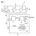
- FIG. 1 shows a receiver circuit 10 which for example, a component of an optical Receiving element forms. This means that the Receiver circuit for processing a measurement signal of a Optoelectronic transducer is suitable.
- the receiver circuit 10 has an input side Amplifier 20 on, at its input E20 a Data signal D is fed to the receiver circuit 10.
- the data signal D is, for example, one in the figure 1, not shown, optoelectronic transducer formed optical reception element.
- the amplifier device 20 has three amplifiers 30, 40 and 50, which are connected in series and thus one Make amplifier chain.
- the seen from the input side first amplifier 30 is a via a control input S30 controllable amplifier.
- a control signal ST at the control input S30 can be the bandwidth and thus determine the noise performance of the amplifier 30.
- the bandwidth and thus the noise behavior of the amplifier 30, for example, by switching a Transimpedance resistance of the amplifier 30 is changed if the amplifier 30 is a Transimpedance amplifier acts.
- a switch of the Operating point of the amplifier 30 as a function of Control signal ST at the control input S30 take place.
- For example may be the current and / or resistors of the amplifier 30th switched over or capacities are switched on.
- the remaining amplifiers 40 and 50 may alternatively also be formed adjustable or adjustable.
- an amplified data signal D ' issued at the output A20 of the amplifier device 20 is of the Amplifier 20 an amplified data signal D ' issued.
- This amplified data signal D ' passes through a Feedback loop to an input E60 a Control device 60.
- the control device 60 has a Control output A60 on, with a control input S20 the Amplifier device 20 and thus with the control terminal S30 of the first amplifier 30 is in communication.
- the optical receiver circuit 10 is like follows: The input side at the Amplifier 20 applied data signal D is from the amplifier device 20 amplified and the output A20 of Amplifier device 20 delivered.
- the data rate f of the amplified data signal D ' is determined by the Control device 60 measured. Subsequently, the generated Control device 60 at its control output A60 the Control signal ST, with which the bandwidth of the first Amplifier 30 is set such that the bandwidth of the first amplifier 30 of the data rate f of the amplified Data signal D 'corresponds. By this is meant that the bandwidth of the first amplifier 30 is as low as is possible and just to amplify the data signal D. sufficient. By setting a minimum possible Bandwidth can be a minimum noise of the amplifier Reach 30, whereby the total noise of Amplifier device 20 is also minimized.
- the control device 60 For generating the control signal ST, the control device 60, a data correlator 70 whose input E70 the Input E60 of the controller 60 forms. On the output side is the data correlator 70 with an input E80 a Bandwidth controller 80 connected.
- the Bandwidth controller 80 has an output A80a on which they enter the data rate of the data signal D ' indicating or characterizing measuring signal M [x: 0] for Display on a monitor or other external Submit ad.
- the bandwidth control device 80 points beyond another output A80b, on which they the one Bandwidth of the data signal D 'indicating or characterizing data rate measurement signal S [0: m] generated and to an input E90 of a downstream state machine 90 emits.
- the state machine 90 has a control input S90, via the State Machine 90 a "start signal” are transmitted can. Such a “start signal” indicates that the optical Receiver circuit 10 is put into operation again. This "Start signal” may e.g. when switching on Receiver circuit can be generated automatically or as needed generated by the system itself ("power on reset").
- An output A90 of the state machine 90 forms the control output A60 of the controller 60.
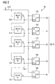
- phase shifter 100 In connection with Figure 2, the operation of the Data correlator 70 is shown.
- the at the input E70 of the data correlator 70 adjacent, amplified Data signal D 'thus first passes through the phase shifter 100 and is phase-shifted by a time t0.
- At the Output of the phase shifter 100 is thus formed phase-shifted auxiliary signal T0.
- the course of the phase-shifted auxiliary signal T0 and to compare the The course of the amplified data signal D ' is shown in FIG. 4 recognizable.
- phase-shifted auxiliary signal T0 passes beyond to the second phase shifter 110 connected to the phase shifter
- 100 is identical and also one Phase shift by the time t0 causes.
- the second phase-shifted auxiliary signal T1 also passes to the third phase shifter 120, to the fourth phase shifter 130 and the fifth phase shifter 135, each one Time shift by more periods t0 cause.
- the output side of the phase shifters are output phase-shifted auxiliary signals T0, T1, T2, T3 and Tn each at a trigger input T of the D flip-flops 150, 160, 170, 180 and 190.
- the trigger inputs T each respond to a positive slope increase; she are therefore triggered on a positive edge.
- the five D-type flip-flops 150, 160, 170, 180 and 190 have each have a D input on, with the amplified Data signal D 'is acted upon.
- the operation of the data correlator 70 is now as follows:
- the data signal D ' reaches the D inputs of the D flip-flops, indicating the respective signal level of the data signal D ' switch on their output, if that at the respective Trigger input T applied phase-shifted auxiliary signal T0, T1, T2, T3 or Tn has a positive edge rise.
- At the outputs of the D flip-flops thus form digital Correlation signals K0, K1, K2, K3 and Kn.
- the time profile of the phase-shifted auxiliary signals T0 to Tn and the digital correlation signals K0 to Kn is shown in FIG.
- the data rate f of the data signal D is selected such that the bit length t BIT of the data signal D is significantly greater than the phase shift or the time interval t0.
- phase shift between the phase-shifted auxiliary signal T0 and the data signal D ' is so small that a high level of the data signal D' is always present when there is an increase in the edge of the phase-shifted auxiliary signal T0.
- the digital correlation signal K0 will thus go to a high level in the presence of a positive edge of the phase-shifted auxiliary signal T0 and remain there unchanged.
- the correlation signal K0 indicates that the phase shift t0 is significantly smaller than the bit length t BIT of the data signal D 'and that therefore: f ⁇ 1 / t0
- the data signal D ' has already changed its signal level and has jumped from a high level to a low level.
- the D flip-flop 170 is thus not switched, so that the digital correlation signal K2 first remains at a low level.
- a reset of the D-type flip-flop 170 to a low level occurs when the data signal D 'after a bit length t bit from a logic high level back to a logic low level.
- the digital correlation signal K2 thus has a rectangular course.
- the correlation signals finally remain there after a first switching to a high level when the associated phase shift is smaller than the bit length t bit of the data signal D (see correlation signals K0 and K1).
- the other correlation signals which relate to phase shifts which are greater than the bit length t bit of the data signal D ', will have a rectangular, that is to say alternating signal course.
- the time profile of the correlation signals K0 to Kn can be used to determine the bit length t bit of the data signal D 'and thus also to determine the data rate f of the data signal D'.
- the cutoff frequency of the low passes is chosen such that this approximately the lower limit frequency of the first Amplifier 30 of the amplifier device 20 according to FIG. 1 equivalent.
- Mean values I0 to In are in downstream comparators 400, 410, 420, 430 and 440 fed respectively on the input side applied time average with a given threshold value S compare. Exceeds the temporal mean the given threshold S, so will at the output of the comparator with a binary threshold signal generated a "high” level. Otherwise, if so time average of the correlation signal the threshold S falls below, is a binary threshold signal with generated a "low” level.
- the generated by the comparators 400, 410, 420, 430 and 440 binary threshold signals carry in the figure 3 the Reference numerals C0, C1, C2, C3 and Cn.
- the threshold value S applied to the comparators is preferably 80% to 95% of the respective "high" level of the Data signal D '.
- a Duty cycle value of about 50% This means that a balanced number of "high” levels and “low” levels occurs. For deviations of a duty cycle value of 50% It can in fact come to errors when a signal sequence with a short "low” level associated with a long "high” level occurs.
- each correlation signal K0 to Kn could under certain circumstances exceed the threshold S, as will be explained below by way of example with reference to the signal I 2 :
- a long sequence of "high” levels causes a rising ramp on the signal I 2 , even if it is long High-level sequence is occasionally interrupted by shorter low-level sequences.If the high levels predominate within a certain period of time, the rising ramp would reach the threshold "S.” This can be seen for example in connection with FIG. in which the course of the signal I 2 is shown ..
- the time constant of the low-pass filters 300, 310, 320, 330 and 340 is selected to be that The same time corresponds in which the number of high levels and the low level.
- the filtering can be done with an analogue or a digital one Low-pass be performed; a digital filtering can done by e.g. the pulse lengths of the correlation signals K0 to Kn are measured.
- the binary threshold signals C0 to Cn form a data rate measurement signal in the thermometer code.
- FIG. 3 shows a decoder 450 on which the binary threshold signals C0 to Cn on the input side.
- the function of the decoder 450 is to do this through the binary threshold signals C0 to Cn formed and im Thermometer code present data rate measurement signal umzucodieren and the output side already in context with the figure 1 explained data rate measurement signal S [0: m] and to form the monitor output signal M [x: 0].
- the State Machine 90 At the Input E90 of the state machine 90 is the part of the Bandwidth controller 80 generated data rate measurement signal S [0: m]. The state machine 90 thus knows, which data rate f the data signal D at the input of the optical Receiver circuit has. In normal operation, the state switches Machine 90, the input-side applied data rate measurement signal S [O: m] at its output A90 and forms the output side the coded control signal ST, the data rate measurement signal S [0: m] corresponds to the bandwidth control device 80.
- the state machine 90 is designed such that they are connected to a "Power on "signal, the control of the amplifier 30 always with the largest data rate begins. This ensures that the amplifier 30 first with the largest bandwidth is operated and thus the maximum possible Input spectrum of the data signal D is amplified.
- Control device 60 alternatively with the unreinforced Data signal D are acted upon and its data rate measure up.
- the control of the amplifier device 20 is regardless of whether the data rate based on the amplified or determined based on the unamplified data signal.
- FIG. 7 shows the signal curves for a data rate f of 0.52 Gbit / s.
- This data rate f corresponds to a bit length t bit of 1.9 ns. Due to the set delay of the three phase shifters 100, 110 and 120 of 1 ns each, the first D flip-flop 150 is reliably triggered and no longer reset. Therefore, the time average I0 of the correlation signal K0 reaches the "high" level of 1 volt.
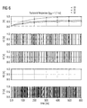
- FIG. 8 shows the simulation result of the signal curves for a data rate f of 0.45 Gbit / s. This data rate corresponds to a bit length t bit of 2.2 ns. Due to the delay of the phase shifters 100, 110 and 120, the first and second D flip-flops 150 and 160 are safely triggered and no longer reset. Therefore, the two time average values I0 and I1 of the two correlation signals K0 and K1 respectively reach the "high" level of 1 volt.
- the time average I2 of the correlation signal K2 does not reach the "high" level.
- the two signals I0 and I1 are the same size, so they are in Figure 8 are badly separated from each other, since their Marked "square” and "rhombus" on top of each other are.
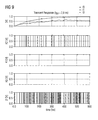
- FIG. 10 shows the simulation result of the signal curves for a data rate of the data signal of 0.312 Gbit / s. This data rate corresponds to a bit length t bit of 3.2 ns. Due to the delay of the phase shifters 100, 110 and 120 according to the figure 2, each of a 1 ns all three D flip-flops 150, 160 and 170 are safely triggered and no longer reset. All three temporal mean values I0, I1 and I2 of the correlation signals K0, K1 and K2 thus reach the "high" level of 1 volt.
- the time average reaches I0 to In one of the correlation signals K0 to Kn the "high" level of 1 volt, the bit length of the data signal D 'must be greater than be the respective phase delay of the correlation signal.
- phase shift of Phase shifter 100 t0 1 ns and reaches the assigned time average I0 of the digital correlation signal K0 the "high" level of one volt, so must the data rate be less than 1 Gbps.
- thermometer code In principle, can be classified by a very finely graduated Delay chain, so by a variety of Phase shifters, D flip-flops, low-pass filters and comparators (see Figures 2 and 3) a very high resolution in the Data rate measurement done.
- the result is one Data rate measurement signal in a thermometer code. to Recoding this thermometer code will - if desired - a thermometer decoder used.
- Threshold preferably in a range between 0.8 times and 0.95 times the "high" level of the data signal D are to provide a reliable data rate determination enable.
- Phase shifter 100, 110, 120, 130 and 135 the same Cause phase shift.
- Phase shift of the phase shifters among themselves also be different, for example, the Phase shift values should be logarithmically staggered.
Landscapes
- Engineering & Computer Science (AREA)
- Computer Networks & Wireless Communication (AREA)
- Signal Processing (AREA)
- Physics & Mathematics (AREA)
- Electromagnetism (AREA)
- Nonlinear Science (AREA)
- Power Engineering (AREA)
- Amplifiers (AREA)
- Optical Communication System (AREA)
- Noise Elimination (AREA)
Abstract
Description
- Figur 1
- ein Ausführungsbeispiel für eine erfindungsgemäße Empfängerschaltung, mit der sich auch das erfindungsgemäße Verfahren zum Betreiben einer Empfängerschaltung sowie das erfindungsgemäße Verfahren zum Charakterisieren der Datenrate eines digitalen Datensignals durchführen lässt;
- Figur 2
- ein Ausführungsbeispiel für einen Datenkorrelator einer Steuereinrichtung der Empfängereinrichtung gemäß Figur 1;
- Figur 3
- ein Ausführungsbeispiel für eine BandbreitenKontrolleinrichtung der Steuereinrichtung der Empfängerschaltung gemäß Figur 1;
- Figur 4
- zeitliche Verläufe der in der Empfängerschaltung gemäß Figur 1 aufretenden Signale sowie
- Figuren 5-10
- beispielhaft Signalverläufe bei einem Betrieb der Empfängerschaltung gemäß Figur 1 bei unterschiedlichen Datenraten.
- 10
- optische Empfängerschaltung
- 20
- Verstärkereinrichtung
- 30
- steuerbarer Verstärker
- 40
- Verstärker
- 50
- Verstärker
- 60
- Steuereinrichtung
- 70
- Datenkorrelator
- 80
- Bandbreitenkontroll-Einrichtung
- 90
- State Machine
- 100,110,120,130,135
- Phasenschieber
- 140
- Punkte
- 150,160,170,180,190
- D-Flip-Flops
- 300,310,320,330,340
- Tiefpässe
- 400,410,420,430,440
- Komparatoren
- 450
- Decoder
Claims (27)
- Empfängerschaltung (10)mit mindestens einer Verstärkereinrichtung (20) zum Verstärken eines eingangsseitig an der Empfängerschaltung (10) anliegenden Datensignals undmit einer Steuereinrichtung (60), die die Datenrate des Datensignals misst und die Bandbreite der Verstärkereinrichtung (20) derart einstellt, dass die Bandbreite der Verstärkereinrichtung (20) der Datenrate des Datensignals entspricht.
- Empfängerschaltung nach Anspruch 1, dadurch gekennzeichnet, dass die Steuereinrichtung (60) eingangsseitig einen Datenkorrelator (70) aufweist, dermit dem Datensignal oder mit dem mit der Verstärkereinrichtung (20) verstärkten Datensignal eingangsseitig beaufschlagt ist,mit dem Datensignal zumindest ein phasenverschobenes Hilfssignal bildet,das Datensignal und das zumindest eine phasenverschobene Hilfssignal einer Autokorrelation unterwirft undausgangsseitig zumindest ein dem Korrelationsergebnis entsprechendes Korrelationssignal zur Bestimmung der Datenrate des Datensignals erzeugt.
- Empfängerschaltung nach Anspruch 2, dadurch gekennzeichnet, dass der Datenkorrelator (70) zur Bildung des zumindest einen phasenverschobenen Hilfssignals einen Phasenschieber (100, 110, 120, 130, 135) und zur Bildung des zumindest einen Korrelationssignals ein D-Flip-Flop (150, 160, 170, 180, 190) aufweist.
- Empfängerschaltung nach Anspruch 3, dadurch gekennzeichnet, dass der Datenkorrelator (70) eine Mehrzahl an Korrelationssignalen erzeugt, die unter Heranziehung einer Mehrzahl an phasenverschobenen Hilfssignalen mit gegenüber dem Datensignal unterschiedlicher Phasenverschiebung gebildet werden.
- Empfängerschaltung nach Anspruch 4, dadurch gekennzeichnet, dass dem Datenkorrelator (70) eine Bandbreiten-Kontrolleinrichtung (80) nachgeordnet ist, die aus den Korrelationssignalen des Datenkorrelators ein Datenrate-Messsignal zur Ansteuerung der Verstärkereinrichtung erzeugt.
- Empfängerschaltung nach Anspruch 5, dadurch gekennzeichnet, dass die Bandbreiten-Kontrolleinrichtung (80) derart ausgestaltet ist, dass sie die Korrelationssignale jeweils zeitlich mittelt und mit jedem gemittelten Korrelationssignal jeweils ein binäres Schwellwertsignal erzeugt, das angibt, ob der zeitliche Mittelwert des jeweiligen Korrelationssignals kleiner oder größer als ein vorgegebener Schwellwert sind.
- Empfängerschaltung nach Anspruch 6, dadurch gekennzeichnet , dass die Bandbreiten-Kontrolleinrichtung (80) zur zeitlichen Mittlung der Korrelationssignale jeweils einen Tiefpass und zur Bildung der binären Schwellwertsignale jeweils einen Komparator aufweist.
- Empfängerschaltung nach Anspruch 6, dadurch gekennzeichnet, dass die Steuereinrichtung (60) eine der Bandbreiten-Kontrolleinrichtung (80) nachgeordnete State Machine (90) aufweist, die unter Berücksichtigung des Datenrate-Messsignals der Bandbreiten-Kontrolleinrichtung die Verstärkereinrichtung ansteuert.
- Empfängerschaltung nach Anspruch 1, dadurch gekennzeichnet, dass die Empfängerschaltung (10) zusätzlich eine Umschaltvorrichtung zum Umschalten des Rauschens bzw. zum Verändern des Rauschverhaltens der Verstärkereinrichtung aufweist.
- Empfängerschaltung nach Anspruch 9, dadurch gekennzeichnet, dass die Umschaltvorrichtung derart ausgestaltet ist, dass sie durch ein Umschalten oder Verändern des Arbeitspunktes der Verstärkereinrichtung die Empfindlichkeit der Empfängerschaltung optimiert.
- Verfahren zum Betreiben einer Empfängerschaltung (10), bei demein Datensignal mit einer Verstärkereinrichtung (20) unter Bildung eines verstärkten Datensignals verstärkt wird,die Datenrate des Datensignals oder die des verstärkten Datensignals gemessen wirdund die Bandbreite der Verstärkereinrichtung (20) derart eingestellt wird, dass die Bandbreite der Verstärkereinrichtung (20) der gemessenen Datenrate entspricht.
- Verfahren nach Anspruch 11, dadurch gekennzeichnet, dass die Datenrate gemessen wird, indemdas Datensignal einer Autokorrelation unter Bildung zumindest eines digitalen Korrelationssignals unterzogen wird,das zumindest eine digitale Korrelationssignal zeitlich gemittelt wird undmit dem zeitlichen Mittelwert ein die Datenrate des Datensignals charakterisierendes Datenratemesssignal erzeugt wird.
- Verfahren nach Anspruch 12, dadurch gekennzeichnet, dass die Autokorrelation durchgeführt wird, indemdas Datensignal unter Bildung mindestens eines phasenverschobenen Hilfssignals phasenverschoben wird unddas Datensignal und das zumindest eine phasenverschobene Hilfssignal unter Bildung des zumindest einen Korrelationssignals korreliert werden.
- Verfahren nach Anspruch 13, dadurch gekennzeichnet, dass die Korrelation des Datensignals und des mindestens einen phasenverschobenen Hilfssignals mit einem D-Flip-Flop erfolgt, indemdas Datensignal an einem D-Eingang des D-Flip-Flops eingespeist wird unddas D-Flip-Flop mit dem mindestens einen phasenverschobenen Hilfssignal auf positive oder negative Flanken getriggert wird, wodurch am Ausgang des D-Flip-Flops das der Phasenverschiebung des Hilfssignals entsprechende Korrelationssignal gebildet wird.
- Verfahren nach Anspruch 13, dadurch gekennzeichnet, dass mit dem zeitlichen Mittelwert des zumindest einen Korrelationssignals ein binäres Schwellwertsignal erzeugt wird, das angibt, ob der zeitliche Mittelwert des zumindest einen Korrelationssignals kleiner oder größer als ein vorgegebener Schwellwert sind.
- Verfahren nach Anspruch 15, dadurch gekennzeichnet, dass der zeitliche Mittelwert des zumindest einen Korrelationssignals jeweils mittels eines Tiefpasses gebildet wird.
- Verfahren nach Anspruch 16, dadurch gekennzeichnet, dass das Schwellwertsignal mit einem Komparator gebildet wird, indem dieser mit dem zeitlichen Mittelwert des Korrelationssignals sowie mit dem vorgegebenen Schwellwert beaufschlagt wird.
- Verfahren nach Anspruch 13, dadurch gekennzeichnet , dasseine Mehrzahl an phasenverschobenen Hilfssignalen erzeugt wird, die gegenüber dem Datensignal unterschiedlich phasenverschoben sind, undmit jedem Hilfssignal jeweils ein digitales Korrelationssignal und ein binäres Schwellwertsignal erzeugt wird.
- Verfahren nach Anspruch 18, dadurch gekennzeichnet, dass mit den Schwellwertsignalen das Datenrate-Messsignal in einem Thermometer-Code erzeugt wird.
- Verfahren zum Charakterisieren der Datenrate eines digitalen Datensignals, bei demdas Datensignal einer Autokorrelation unter Bildung zumindest eines digitalen Korrelationssignals unterzogen wird,das zumindest eine digitale Korrelationssignal einer zeitlichen Mittelwertbildung unterzogen wird undmit dem zeitlichen Mittelwert ein die Datenrate des Datensignals charakterisierendes Datenrate-Messsignal erzeugt wird.
- Verfahren nach Anspruch 20, dadurch gekennzeichnet, dass die Autokorrelation durchgeführt wird, indemdas Datensignal unter Bildung mindestens eines phasenverschobenen Hilfssignals phasenverschoben wird unddas Datensignal und das zumindest eine phasenverschobene Hilfssignal unter Bildung des zumindest einen Korrelationssignals korreliert werden.
- Verfahren nach Anspruch 20, dadurch gekennzeichnet, dass mit dem zeitlichen Mittelwert des zumindest einen Korrelationssignals ein binäres Schwellwertsignal erzeugt wird, das angibt, ob der zeitliche Mittelwert des zumindest einen Korrelationssignals kleiner oder größer als ein vorgegebener Schwellwert ist.
- Verfahren nach Anspruch 22, dadurch gekennzeichnet , dasseine Mehrzahl an phasenverschobenen Hilfssignalen erzeugt wird, die gegenüber dem Datensignal unterschiedlich phasenverschoben sind, undmit jedem Hilfssignal jeweils ein digitales Korrelationssignal und ein binäres Schwellwertsignal erzeugt wird.
- Verfahren nach Anspruch 23, dadurch gekennzeichnet , dass mit den Schwellwertsignalen das Datenrate-Messsignal in einem Thermometer-Code erzeugt wird.
- Verfahren nach Anspruch 24, dadurch gekennzeichnet, dass die Korrelation des Datensignals und der phasenverschobenen Hilfssignale jeweils mit einem D-Flip-Flop erfolgt, indemdas Datensignal an einem D-Eingang des jeweiligen D-Flip-Flops eingespeist wird unddas jeweilige D-Flip-Flop mit dem jeweiligen phasenverschobenen Hilfssignal auf positive oder negative Flanken getriggert wird, wodurch am Ausgang des jeweiligen D-Flip-Flops jeweils das der Phasenverschiebung des jeweiligen Hilfssignals entsprechende Korrelationssignal gebildet wird.
- Verfahren nach Anspruch 24, dadurch gekennzeichnet, dass die zeitlichen Mittelwerte der Korrelationssignale jeweils mittels eines Tiefpasses gebildet werden.
- Verfahren nach Anspruch 24, dadurch gekennzeichnet, dass die Schwellwertsignale jeweils mit einem Komparator gebildet werden, indem dieser mit dem zeitlichen Mittelwert des jeweiligen Korrelationssignals sowie mit dem vorgegebenen Schwellwert beaufschlagt wird.
Applications Claiming Priority (2)
| Application Number | Priority Date | Filing Date | Title |
|---|---|---|---|
| US54075904P | 2004-01-30 | 2004-01-30 | |
| US540759P | 2004-01-30 |
Publications (3)
| Publication Number | Publication Date |
|---|---|
| EP1562312A2 true EP1562312A2 (de) | 2005-08-10 |
| EP1562312A3 EP1562312A3 (de) | 2006-03-08 |
| EP1562312B1 EP1562312B1 (de) | 2008-05-21 |
Family
ID=34676904
Family Applications (1)
| Application Number | Title | Priority Date | Filing Date |
|---|---|---|---|
| EP05090014A Expired - Lifetime EP1562312B1 (de) | 2004-01-30 | 2005-01-28 | Empfängerschaltung sowie Verfahren zu deren Betrieb |
Country Status (3)
| Country | Link |
|---|---|
| US (1) | US7483499B2 (de) |
| EP (1) | EP1562312B1 (de) |
| DE (1) | DE502005004158D1 (de) |
Families Citing this family (5)
| Publication number | Priority date | Publication date | Assignee | Title |
|---|---|---|---|---|
| US7778351B2 (en) * | 2002-04-09 | 2010-08-17 | International Business Machines Corporation | Tunable CMOS receiver apparatus |
| DE102005061947B4 (de) * | 2005-12-23 | 2008-07-10 | Qimonda Ag | Synchronisationsverfahren sowie entsprechende Vorrichtung und Digitalschaltung und ein Automat zur Synchronisation einer Digitalschaltung |
| KR101459147B1 (ko) * | 2008-02-04 | 2014-11-10 | 엘지전자 주식회사 | 무선통신 시스템에서 전송 파워 제어 명령 전송 방법 |
| US10419063B2 (en) * | 2016-12-30 | 2019-09-17 | Waviot Integrated Systems, Llc | Method and system for receiving telemetry messages over RF channel |
| EP3632067B1 (de) * | 2018-08-20 | 2023-10-25 | Waviot Integrated Systems, LLC | Verfahren und system zum empfangen von telemetrienachrichten über einen hf-kanal |
Family Cites Families (15)
| Publication number | Priority date | Publication date | Assignee | Title |
|---|---|---|---|---|
| US4608542A (en) * | 1985-06-06 | 1986-08-26 | Rca Corporation | Bandwidth controlled data amplifier |
| US5088107A (en) * | 1989-10-27 | 1992-02-11 | Crystal Semiconductor | Linear channel bandwidth calibration circuit |
| US5864416A (en) * | 1996-10-02 | 1999-01-26 | Harris Corporation | Tuning optical communications receiver by controlling drain current input to variable transconductance fet stage of variable bandwidth transimpedance amplifier |
| US5892472A (en) * | 1997-06-30 | 1999-04-06 | Harris Corporation | Processor controlled analog-to-digital converter circuit |
| US6266172B1 (en) * | 1997-11-06 | 2001-07-24 | Agere Systems Optoelectronics Guardian Corp. | Signal bit rate and performance measurement for optical channel signals |
| US6377618B1 (en) * | 1998-12-30 | 2002-04-23 | Agere Systems Guardian Corp. | Auto-correlation system and method for rate detection of a data communication channel |
| US6904290B1 (en) * | 1999-09-30 | 2005-06-07 | Telefonaktiebolaget L M Ericsson (Publ) | Method and apparatus for transmit power control |
| SE520433C2 (sv) * | 2000-12-01 | 2003-07-08 | Transmode Systems Ab | Förstärkarkrets, ett optiskt kommunikationssystem och en metod för att styra förstärkning |
| US6928249B2 (en) * | 2001-02-15 | 2005-08-09 | Agilent Technologies, Inc. | Fiber optic receiver with an adjustable response preamplifier |
| JP3599001B2 (ja) * | 2001-06-25 | 2004-12-08 | ソニー株式会社 | 自動利得制御回路およびその方法、並びにそれらを用いた復調装置 |
| US6933786B1 (en) * | 2002-05-15 | 2005-08-23 | Cypress Semiconductor Corporation | Amplifier circuit and method |
| US7130602B2 (en) * | 2002-10-31 | 2006-10-31 | Qualcomm Incorporated | Dynamically programmable receiver |
| US20050046482A1 (en) * | 2003-08-27 | 2005-03-03 | Karl Schrodinger | Receiver circuit |
| US6876260B2 (en) * | 2003-09-09 | 2005-04-05 | Gennum Corporation | Elevated front-end transimpedance amplifier |
| US20050135756A1 (en) * | 2003-12-19 | 2005-06-23 | Chao Zhang | Bi-directional optical transceiver module having automatic-restoring unlocking mechanism |
-
2004
- 2004-04-09 US US10/821,349 patent/US7483499B2/en not_active Expired - Fee Related
-
2005
- 2005-01-28 EP EP05090014A patent/EP1562312B1/de not_active Expired - Lifetime
- 2005-01-28 DE DE502005004158T patent/DE502005004158D1/de not_active Expired - Lifetime
Also Published As
| Publication number | Publication date |
|---|---|
| EP1562312A3 (de) | 2006-03-08 |
| US7483499B2 (en) | 2009-01-27 |
| EP1562312B1 (de) | 2008-05-21 |
| DE502005004158D1 (de) | 2008-07-03 |
| US20050169407A1 (en) | 2005-08-04 |
Similar Documents
| Publication | Publication Date | Title |
|---|---|---|
| DE60001444T2 (de) | Verfahren und Vorrichtung zur Übergangsregelungsstabilzierung in optisch verstärkten Netzwerken | |
| DE69527931T2 (de) | Ausgangssteuerschaltung für eine Übertragungsleistungsschaltung | |
| DE69833584T2 (de) | Vorrichtung und Verfahren zum Empfang von optischen Burstsignalen | |
| DE19882819B4 (de) | Optische Empfangsvorrichtung | |
| CH662022A5 (de) | Verfahren und einrichtung zur ueberwachung einer digitalen uebertragungsanlage. | |
| DE69414642T2 (de) | Vorrichtung zur automatischen Verstärkungsregelung | |
| DE69720948T2 (de) | Radioempfänger mit Detektor für Unterführungen | |
| DE102015217695B4 (de) | Kommunikationsvorrichtung mit Antennen-Dämpfungskompensation | |
| DE60309969T2 (de) | Optische Übertragungseinrichtung und optisches Übertragungsverfahren für ein Burst-Funksignal | |
| DE2849343A1 (de) | Schaltung zur automatischen regelung des verstaerkungsfaktors eines empfangskanals | |
| DE60221824T2 (de) | System mit einer schaltung und verfahren zum umschalten der verstärkung eines vorverstärkers | |
| EP1562312A2 (de) | Empfängerschaltung sowie Verfahren zu deren Betrieb | |
| EP2283594B1 (de) | Infrarot-empfängerschaltung | |
| DE60115157T2 (de) | Automatische Verstärkungsschleife mit kurzer Ansprechzeit für schmalbandige Systeme | |
| EP1445747B1 (de) | Verfahren zum Übertragen von Steuerbefehlen von einem Sendeelement zu einem Messtaster | |
| DE102009045220A1 (de) | System und Verfahren zum Begrenzen von Stromoszillationen | |
| DE602005004546T2 (de) | Verfahren zur Verstärkung eines zeitvariablen optischen Signals und optische Verstärkungseinrichtung | |
| EP1662625B1 (de) | Treiberschaltung mit selbständiger Offsetkompensation eines Verstärkers und Verfahren zur Offsetkompensation eines Verstärkers einer Treiberschaltung | |
| DE19637151C1 (de) | Schaltung zur Ermittlung und Speicherung eines Signalmittelwertes | |
| EP1879092B1 (de) | Verfahren zum Regeln einer Busgerätespannung und Vorschalteinrichtung | |
| EP1684457B1 (de) | Spannungsversorgungsvorrichtung für einen Buskoppler und entsprechendes Betriebsverfahren | |
| DE2456577C3 (de) | Breitbandige Verstärkeranordnung für intermittierende Signale | |
| DE3136629C2 (de) | ||
| EP1598959B1 (de) | Optisches Sendemodul | |
| EP0735679B1 (de) | Flankendetektor |
Legal Events
| Date | Code | Title | Description |
|---|---|---|---|
| PUAI | Public reference made under article 153(3) epc to a published international application that has entered the european phase |
Free format text: ORIGINAL CODE: 0009012 |
|
| AK | Designated contracting states |
Kind code of ref document: A2 Designated state(s): AT BE BG CH CY CZ DE DK EE ES FI FR GB GR HU IE IS IT LI LT LU MC NL PL PT RO SE SI SK TR |
|
| AX | Request for extension of the european patent |
Extension state: AL BA HR LV MK YU |
|
| RIC1 | Information provided on ipc code assigned before grant |
Ipc: 7H 04B 10/158 A Ipc: 7H 04L 25/02 B |
|
| PUAL | Search report despatched |
Free format text: ORIGINAL CODE: 0009013 |
|
| AK | Designated contracting states |
Kind code of ref document: A3 Designated state(s): AT BE BG CH CY CZ DE DK EE ES FI FR GB GR HU IE IS IT LI LT LU MC NL PL PT RO SE SI SK TR |
|
| AX | Request for extension of the european patent |
Extension state: AL BA HR LV MK YU |
|
| RIC1 | Information provided on ipc code assigned before grant |
Ipc: H04L 1/00 20060101ALI20060113BHEP Ipc: H04L 25/02 20060101ALI20060113BHEP Ipc: H04B 10/158 20060101AFI20050620BHEP |
|
| 17P | Request for examination filed |
Effective date: 20060323 |
|
| AKX | Designation fees paid |
Designated state(s): DE FR GB |
|
| GRAP | Despatch of communication of intention to grant a patent |
Free format text: ORIGINAL CODE: EPIDOSNIGR1 |
|
| GRAS | Grant fee paid |
Free format text: ORIGINAL CODE: EPIDOSNIGR3 |
|
| GRAA | (expected) grant |
Free format text: ORIGINAL CODE: 0009210 |
|
| AK | Designated contracting states |
Kind code of ref document: B1 Designated state(s): DE FR GB |
|
| REG | Reference to a national code |
Ref country code: GB Ref legal event code: FG4D Free format text: NOT ENGLISH |
|
| REF | Corresponds to: |
Ref document number: 502005004158 Country of ref document: DE Date of ref document: 20080703 Kind code of ref document: P |
|
| PLBE | No opposition filed within time limit |
Free format text: ORIGINAL CODE: 0009261 |
|
| STAA | Information on the status of an ep patent application or granted ep patent |
Free format text: STATUS: NO OPPOSITION FILED WITHIN TIME LIMIT |
|
| 26N | No opposition filed |
Effective date: 20090224 |
|
| GBPC | Gb: european patent ceased through non-payment of renewal fee |
Effective date: 20090128 |
|
| REG | Reference to a national code |
Ref country code: FR Ref legal event code: ST Effective date: 20091030 |
|
| PG25 | Lapsed in a contracting state [announced via postgrant information from national office to epo] |
Ref country code: GB Free format text: LAPSE BECAUSE OF NON-PAYMENT OF DUE FEES Effective date: 20090128 |
|
| PG25 | Lapsed in a contracting state [announced via postgrant information from national office to epo] |
Ref country code: FR Free format text: LAPSE BECAUSE OF NON-PAYMENT OF DUE FEES Effective date: 20090202 |
|
| PGFP | Annual fee paid to national office [announced via postgrant information from national office to epo] |
Ref country code: DE Payment date: 20160317 Year of fee payment: 12 |
|
| REG | Reference to a national code |
Ref country code: DE Ref legal event code: R119 Ref document number: 502005004158 Country of ref document: DE |
|
| PG25 | Lapsed in a contracting state [announced via postgrant information from national office to epo] |
Ref country code: DE Free format text: LAPSE BECAUSE OF NON-PAYMENT OF DUE FEES Effective date: 20170801 |