EP1562287A1 - Verfahren und Schaltung zum Phasenabgleich von Verstärkermodulen - Google Patents
Verfahren und Schaltung zum Phasenabgleich von Verstärkermodulen Download PDFInfo
- Publication number
- EP1562287A1 EP1562287A1 EP04030213A EP04030213A EP1562287A1 EP 1562287 A1 EP1562287 A1 EP 1562287A1 EP 04030213 A EP04030213 A EP 04030213A EP 04030213 A EP04030213 A EP 04030213A EP 1562287 A1 EP1562287 A1 EP 1562287A1
- Authority
- EP
- European Patent Office
- Prior art keywords
- amplifier
- module
- phase
- vmn
- modules
- Prior art date
- Legal status (The legal status is an assumption and is not a legal conclusion. Google has not performed a legal analysis and makes no representation as to the accuracy of the status listed.)
- Granted
Links
- 238000000034 method Methods 0.000 title claims abstract description 20
- 239000012071 phase Substances 0.000 description 28
- 238000004519 manufacturing process Methods 0.000 description 3
- 230000032683 aging Effects 0.000 description 2
- 230000001419 dependent effect Effects 0.000 description 1
- 230000002349 favourable effect Effects 0.000 description 1
- 239000007790 solid phase Substances 0.000 description 1
Images
Classifications
-
- H—ELECTRICITY
- H03—ELECTRONIC CIRCUITRY
- H03F—AMPLIFIERS
- H03F3/00—Amplifiers with only discharge tubes or only semiconductor devices as amplifying elements
- H03F3/60—Amplifiers in which coupling networks have distributed constants, e.g. with waveguide resonators
- H03F3/602—Combinations of several amplifiers
-
- H—ELECTRICITY
- H03—ELECTRONIC CIRCUITRY
- H03F—AMPLIFIERS
- H03F3/00—Amplifiers with only discharge tubes or only semiconductor devices as amplifying elements
- H03F3/20—Power amplifiers, e.g. Class B amplifiers, Class C amplifiers
- H03F3/21—Power amplifiers, e.g. Class B amplifiers, Class C amplifiers with semiconductor devices only
- H03F3/211—Power amplifiers, e.g. Class B amplifiers, Class C amplifiers with semiconductor devices only using a combination of several amplifiers
Definitions
- the invention relates to a method for adjusting phases of amplifier modules according to the preamble of patent claim 1, as well as a circuit according to the preamble of claim 5.
- a Another object is to provide a circuit for carrying out the method.
- an amplifier module as a reference module determined with a solid phase.
- a second and in further steps will be the phases of the other amplifier modules in pairs with those in the first Step specific reference module set so that the combined output power minimal from the respective individual amplifier module and the reference module becomes.
- the phase of the reference module is rotated by 180 °.
- a circuit according to the invention for balancing the phases of a number of Amplifier modules include a signal source associated with each amplifier stage is.
- a digital interface connected to the signal source.
- An advantage of the method according to the invention is that during production no phase adjustment the amplifier modules on a separate exemplary reference module is necessary.
- the amplifier modules may suitably transmitter modules in an antenna system be.
- phase adjustment can be done essentially automatically.
- a compensation of phase deviations can be achieved with the method according to the invention, which arise, for example, due to temperature changes or aging or replacement of an amplifier module.
- the phase adjustment can be done during operation of the amplifier modules.
- a further advantage of the method according to the invention is that the result of the phase adjustment is independent of the reference module selected in the first method step.
- phase for each Amplifier module digitally generated and set. This is compared to an analog Generation of more precise phase values adjustable.
- the phase values digitally set much faster, eliminating the entire phasing can be done faster.
- phase value at which the combined output power from the respective individual amplifier module and the reference module is minimal stored is minimal stored. This makes it possible for a system restart of the amplifier modules the phase values can be written back to the amplifier modules.
- the phase value can also be assigned to the amplifier stage Signal source to be written.
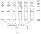
- Each amplifier module VM1-VMn is assigned a signal source M1-Mn, wherein the signal source M1-Mn respectively to the input IN of the amplifier module VM1-VMn connected is.
- the outputs OUT of the amplifier modules VM1-VM6 are equipped with a Summator SUM connected. In summer SUM, the output powers become the individual amplifier modules VM1-VM6 combined.
- the amplifier modules are matched in pairs, wherein all other modules are switched off during the adjustment except for the two modules to be adjusted.
- the phase of any amplifier module hereinafter referred to as reference module, is initialized and kept constant during the calibration procedure.
- the remaining modules are connected individually and expediently in sequence.
- the gain module VM1 is selected as the reference module.
- VM1 VM2 VM3 VM4 VM5 VM6 Step 1 one one x x x x x 2nd step one x one x x x 3rd step one x x one x x 4th step one x x x one x 5th step one x x x x one
- the phase of the respectively second amplifier module VM2-VM6 is increased from zero until a power minimum of the output power is measured at the output of the summer.
- the associated phase value of the corresponding amplifier module VM2-VM6 is stored (not shown).
- the adjustment to the power minimum is more favorable than a comparison to the power maximum, since the minimum on the phase adjustment is significantly sharper.
- the inventive method is applicable in antenna systems with or several channels.
Landscapes
- Engineering & Computer Science (AREA)
- Power Engineering (AREA)
- Amplifiers (AREA)
Abstract
Description
Ein Nachteil dieses Verfahrens ist, dass in der Serienproduktion von Bauteilen mit mehreren parallel geschalteten Verstärkermodulen ein erhöhter Abgleichaufwand nötig ist. Ein weiterer Nachteil ist, dass Phasenfehler, welche z.B. aufgrund von Temperaturveränderungen oder Alterung auftreten, nicht ausgeglichen werden können.
Ein weiterer Vorteil des erfindungsgemäßen Verfahrens ist, dass das Ergebnis des Phasenabgleichs unabhängig von dem im ersten Verfahrensschritt ausgewählten Referenzmoduls ist.
Die Phase eines beliebigen Verstärkermoduls, im weiteren als Referenzmodul bezeichnet, wird initialisiert und während der Abgleichprozedur konstant gehalten. Die übrigen Module werden einzeln und zweckmäßig der Reihe nach hinzugeschaltet.
| VM1 | VM2 | VM3 | VM4 | VM5 | VM6 | |
| 1. Schritt | ein | ein | x | x | x | x |
| 2. Schritt | ein | x | ein | x | x | x |
| 3. Schritt | ein | x | x | ein | x | x |
| 4. Schritt | ein | x | x | x | ein | x |
| 5. Schritt | ein | x | x | x | x | ein |
Der Abgleich auf das Leistungsminimum ist günstiger als ein Abgleich auf das Leistungsmaximum, da das Minimum über die Phaseneinstellung deutlich schärfer ausgeprägt ist. Nach Abschluß des Phasenabgleichs, d.h. alle Verstärkermodule VM2-VM6 wurden mit dem Referenzmodul VM1 abgeglichen, wird die Phase des als Referenzmoduls festgelegten Verstärkermoduls VM1 um 180° gedreht. Anschließend werden alle Verstärkermodule aktiviert.
Claims (6)
- Verfahren zum Abgleichen der Phasen einer Anzahl von Verstärkermodulen (VM1,...,VMn) mittels eines Referenzmoduls (VM1) zur Maximierung der kombinierten Ausgangsleistung der Verstärkermodule (VM1,...,VMn), dadurch gekennzeichnet, dass in einem ersten Schritt ein Verstärkermodul (VM1) als Referenzmodul mit einer festen Phase bestimmt wird, dass in einem zweiten und in weiteren Schritten die Phasen der anderen Verstärkermodule (VM2,...,VMn) jeweils paarweise mit dem im ersten Schritt bestimmten Referenzmodul (VM1) derart eingestellt werden, dass die kombinierte Ausgangsleistung aus dem jeweiligen einzelnen Verstärkermodul (VM2,...,VMn) und dem Referenzmodul (VM1) minimal wird und dass in einem letzten Schritt die Phase des Referenzmoduls (VM1) um 180° gedreht wird.
- Verfahren nach Anspruch 1, dadurch gekennzeichnet, dass vor einem Phasenabgleich zwischen dem Referenzmodul (VM1) und einem Verstärkermodul (VM2,...,VMn) die übrigen Verstärkermodule ausgeschaltet werden.
- Verfahren nach einem der vorangehenden Ansprüche, dadurch gekennzeichnet, dass die Phase für jedes Verstärkermodul (VM1,...,VMn) digital erzeugt und eingestellt wird.
- Verfahren nach einem der vorangehenden Ansprüche, dadurch gekennzeichnet, dass der Phasenwert, bei dem die kombinierte Ausgangsleistung aus dem jeweiligen einzelnen Verstärkermodul (VM2,...,VMn) und dem Referenzmodul (VM1) minimal ist, gespeichert wird.
- Schaltung zum Abgleichen der Phasen einer Anzahl von Verstärkermodulen (VM1,...,VMn) nach einem Verfahren gemäß einem der vorangehenden Ansprüche, dadurch gekennzeichnet, dass jeder Verstärkerstufe (VM1,...,VMn) eine Signalquelle (M1,...,Mn) mit einer einstellbaren Phase zugeordnet ist.
- Schaltung nach Anspruch 5, dadurch gekennzeichnet, dass eine mit der Signalquelle (M1,...,Mn) verbundene digitale Schnittstelle vorhanden ist.
Applications Claiming Priority (2)
| Application Number | Priority Date | Filing Date | Title |
|---|---|---|---|
| DE102004006070A DE102004006070B3 (de) | 2004-02-07 | 2004-02-07 | Verfahren und Schaltung zum Phasenabgleich von Verstärkermodulen |
| DE102004006070 | 2004-02-07 |
Publications (2)
| Publication Number | Publication Date |
|---|---|
| EP1562287A1 true EP1562287A1 (de) | 2005-08-10 |
| EP1562287B1 EP1562287B1 (de) | 2006-08-09 |
Family
ID=34683975
Family Applications (1)
| Application Number | Title | Priority Date | Filing Date |
|---|---|---|---|
| EP04030213A Ceased EP1562287B1 (de) | 2004-02-07 | 2004-12-21 | Verfahren und Schaltung zum Phasenabgleich von Verstärkermodulen |
Country Status (3)
| Country | Link |
|---|---|
| US (1) | US7230478B2 (de) |
| EP (1) | EP1562287B1 (de) |
| DE (2) | DE102004006070B3 (de) |
Families Citing this family (3)
| Publication number | Priority date | Publication date | Assignee | Title |
|---|---|---|---|---|
| US8843088B2 (en) | 2008-10-15 | 2014-09-23 | Apple Inc. | Minimum feedback radio architecture with digitally configurable adaptive linearization |
| US8213880B2 (en) * | 2008-10-15 | 2012-07-03 | Rockstar Bidco, LP | Minimum feedback radio architecture with digitally configurable adaptive linearization |
| US20140152389A1 (en) * | 2011-07-25 | 2014-06-05 | Andrew Llc | Actively Tuned Circuit Having Parallel Carrier and Peaking Paths |
Citations (1)
| Publication number | Priority date | Publication date | Assignee | Title |
|---|---|---|---|---|
| WO2001006643A1 (en) * | 1999-07-20 | 2001-01-25 | Qualcomm Incorporated | Parallel amplifier architecture using digital phase control techniques |
Family Cites Families (3)
| Publication number | Priority date | Publication date | Assignee | Title |
|---|---|---|---|---|
| DE1913670A1 (de) * | 1969-03-18 | 1970-09-24 | Siemens Ag | Einrichtung zur Erzeugung elektromagnetischer Schwingungsenergie,insbesondere im Mikrowellenbereich |
| US6006111A (en) * | 1997-10-08 | 1999-12-21 | Nortel Networks Corporation | Self-balancing matrix amplifier |
| JP2001094350A (ja) * | 1999-08-31 | 2001-04-06 | Samsung Electronics Co Ltd | 携帯電話端末用電力増幅器 |
-
2004
- 2004-02-07 DE DE102004006070A patent/DE102004006070B3/de not_active Expired - Fee Related
- 2004-12-21 EP EP04030213A patent/EP1562287B1/de not_active Ceased
- 2004-12-21 DE DE502004001153T patent/DE502004001153D1/de not_active Expired - Lifetime
-
2005
- 2005-02-04 US US11/049,669 patent/US7230478B2/en not_active Expired - Fee Related
Patent Citations (1)
| Publication number | Priority date | Publication date | Assignee | Title |
|---|---|---|---|---|
| WO2001006643A1 (en) * | 1999-07-20 | 2001-01-25 | Qualcomm Incorporated | Parallel amplifier architecture using digital phase control techniques |
Also Published As
| Publication number | Publication date |
|---|---|
| DE102004006070B3 (de) | 2005-09-22 |
| DE502004001153D1 (de) | 2006-09-21 |
| US7230478B2 (en) | 2007-06-12 |
| EP1562287B1 (de) | 2006-08-09 |
| US20050189991A1 (en) | 2005-09-01 |
Similar Documents
| Publication | Publication Date | Title |
|---|---|---|
| DE60317371T2 (de) | Verstärkung mit hohem wirkungsgrad | |
| DE2904786C2 (de) | Verfahren zur Regelung von Wechselrichtern im Parallelbetrieb und Schaltungsanordnungen zur Durchführung des Verfahrens | |
| DE102007044131B4 (de) | Speichersteuerung und Speichersystem mit einer Speichersteuerung und einer Speicherschaltung | |
| DE2710517A1 (de) | Steuersystem mit zwei oder mehr kanaelen | |
| DE102012222065A1 (de) | Parallelwechselrichter-vorrichtung | |
| DE19905826A1 (de) | Vorrichtung zum gleichzeitigen Verstärken mehrerer Signale | |
| DE3006451A1 (de) | Bearbeitungsschaltung fuer antennensignale | |
| DE112014002276T5 (de) | Modularer konfigurierbarer Multimegawatt-Leistungsverstärker | |
| EP0825707B1 (de) | Lastausgleichsregelung von mehreren Antrieben | |
| DE60027989T2 (de) | Leistungsverstärkersystem für ein Antennensystem | |
| EP1562287B1 (de) | Verfahren und Schaltung zum Phasenabgleich von Verstärkermodulen | |
| DE10304872B3 (de) | Konvertieranordnung, Verfahren zum Konvertieren eines Thermometercodes und Analog-Digital-Wandler | |
| DE102014003168A1 (de) | Steuereinrichtung für einen Servomotor | |
| DE102023124968A1 (de) | Verfahren zur Schrupp- oder Schruppdrehbearbeitung mit optimierten Prozessparametern | |
| DE3219923A1 (de) | Signalsystem mit aehnlichen redundanzsignalen | |
| DE3707143C2 (de) | ||
| DE102008007100A1 (de) | Verfahren und Vorrichtung zur Stromregelung oder Momentenregelung | |
| DE10219657A1 (de) | Lautsprechersystem | |
| DE102019133807A1 (de) | Eingebettetes system zur umgebungskontrolle und lebenserhaltung mit kompaktem formfaktor | |
| DE69122647T2 (de) | Informationssignalverarbeitungsmethode und -apparat | |
| DE3346179C2 (de) | ||
| DE102022202068A1 (de) | Verfahren zum Bestimmen einer E/E-Architektur eines Fahrzeugs | |
| DE1205738B (de) | Schaltungsanordnung zur Fehlerkorrektur binaer verschluesselter Datenwoerter | |
| EP1777078B2 (de) | Verfahren zur Verarbeitung von Druckprodukten zu Druckerzeugnissen in Chargen sich folgender unterschiedlicher Fertigungsaufträge | |
| DE102016007721A1 (de) | Servosteuerungssystem mit der Funktion zum Schalten eines Lernspeichers |
Legal Events
| Date | Code | Title | Description |
|---|---|---|---|
| PUAI | Public reference made under article 153(3) epc to a published international application that has entered the european phase |
Free format text: ORIGINAL CODE: 0009012 |
|
| AK | Designated contracting states |
Kind code of ref document: A1 Designated state(s): AT BE BG CH CY CZ DE DK EE ES FI FR GB GR HU IE IS IT LI LT LU MC NL PL PT RO SE SI SK TR |
|
| AX | Request for extension of the european patent |
Extension state: AL BA HR LV MK YU |
|
| 17P | Request for examination filed |
Effective date: 20051014 |
|
| GRAP | Despatch of communication of intention to grant a patent |
Free format text: ORIGINAL CODE: EPIDOSNIGR1 |
|
| AKX | Designation fees paid |
Designated state(s): DE FR GB IT |
|
| GRAS | Grant fee paid |
Free format text: ORIGINAL CODE: EPIDOSNIGR3 |
|
| GRAA | (expected) grant |
Free format text: ORIGINAL CODE: 0009210 |
|
| AK | Designated contracting states |
Kind code of ref document: B1 Designated state(s): DE FR GB IT |
|
| REG | Reference to a national code |
Ref country code: GB Ref legal event code: FG4D Free format text: NOT ENGLISH |
|
| REF | Corresponds to: |
Ref document number: 502004001153 Country of ref document: DE Date of ref document: 20060921 Kind code of ref document: P |
|
| GBT | Gb: translation of ep patent filed (gb section 77(6)(a)/1977) |
Effective date: 20061030 |
|
| ET | Fr: translation filed | ||
| PLBE | No opposition filed within time limit |
Free format text: ORIGINAL CODE: 0009261 |
|
| STAA | Information on the status of an ep patent application or granted ep patent |
Free format text: STATUS: NO OPPOSITION FILED WITHIN TIME LIMIT |
|
| 26N | No opposition filed |
Effective date: 20070510 |
|
| REG | Reference to a national code |
Ref country code: DE Ref legal event code: R081 Ref document number: 502004001153 Country of ref document: DE Owner name: AIRBUS DEFENCE AND SPACE GMBH, DE Free format text: FORMER OWNER: EADS DEUTSCHLAND GMBH, 85521 OTTOBRUNN, DE Effective date: 20140916 Ref country code: DE Ref legal event code: R081 Ref document number: 502004001153 Country of ref document: DE Owner name: AIRBUS DS ELECTRONICS AND BORDER SECURITY GMBH, DE Free format text: FORMER OWNER: EADS DEUTSCHLAND GMBH, 85521 OTTOBRUNN, DE Effective date: 20140916 Ref country code: DE Ref legal event code: R081 Ref document number: 502004001153 Country of ref document: DE Owner name: HENSOLDT SENSORS GMBH, DE Free format text: FORMER OWNER: EADS DEUTSCHLAND GMBH, 85521 OTTOBRUNN, DE Effective date: 20140916 |
|
| REG | Reference to a national code |
Ref country code: FR Ref legal event code: PLFP Year of fee payment: 12 |
|
| REG | Reference to a national code |
Ref country code: DE Ref legal event code: R081 Ref document number: 502004001153 Country of ref document: DE Owner name: AIRBUS DS ELECTRONICS AND BORDER SECURITY GMBH, DE Free format text: FORMER OWNER: AIRBUS DEFENCE AND SPACE GMBH, 85521 OTTOBRUNN, DE Ref country code: DE Ref legal event code: R081 Ref document number: 502004001153 Country of ref document: DE Owner name: HENSOLDT SENSORS GMBH, DE Free format text: FORMER OWNER: AIRBUS DEFENCE AND SPACE GMBH, 85521 OTTOBRUNN, DE |
|
| REG | Reference to a national code |
Ref country code: FR Ref legal event code: PLFP Year of fee payment: 13 |
|
| REG | Reference to a national code |
Ref country code: DE Ref legal event code: R082 Ref document number: 502004001153 Country of ref document: DE Representative=s name: LIFETECH IP SPIES & BEHRNDT PATENTANWAELTE PAR, DE Ref country code: DE Ref legal event code: R081 Ref document number: 502004001153 Country of ref document: DE Owner name: HENSOLDT SENSORS GMBH, DE Free format text: FORMER OWNER: AIRBUS DS ELECTRONICS AND BORDER SECURITY GMBH, 82024 TAUFKIRCHEN, DE |
|
| REG | Reference to a national code |
Ref country code: FR Ref legal event code: PLFP Year of fee payment: 14 |
|
| PGFP | Annual fee paid to national office [announced via postgrant information from national office to epo] |
Ref country code: DE Payment date: 20171211 Year of fee payment: 14 Ref country code: FR Payment date: 20171221 Year of fee payment: 14 |
|
| PGFP | Annual fee paid to national office [announced via postgrant information from national office to epo] |
Ref country code: GB Payment date: 20171221 Year of fee payment: 14 |
|
| PGFP | Annual fee paid to national office [announced via postgrant information from national office to epo] |
Ref country code: IT Payment date: 20171221 Year of fee payment: 14 |
|
| REG | Reference to a national code |
Ref country code: DE Ref legal event code: R119 Ref document number: 502004001153 Country of ref document: DE |
|
| GBPC | Gb: european patent ceased through non-payment of renewal fee |
Effective date: 20181221 |
|
| PG25 | Lapsed in a contracting state [announced via postgrant information from national office to epo] |
Ref country code: FR Free format text: LAPSE BECAUSE OF NON-PAYMENT OF DUE FEES Effective date: 20181231 Ref country code: DE Free format text: LAPSE BECAUSE OF NON-PAYMENT OF DUE FEES Effective date: 20190702 Ref country code: IT Free format text: LAPSE BECAUSE OF NON-PAYMENT OF DUE FEES Effective date: 20181221 |
|
| PG25 | Lapsed in a contracting state [announced via postgrant information from national office to epo] |
Ref country code: GB Free format text: LAPSE BECAUSE OF NON-PAYMENT OF DUE FEES Effective date: 20181221 |