EP1560950B1 - A crystal puller and method for growing a monocrystalline ingot - Google Patents
A crystal puller and method for growing a monocrystalline ingot Download PDFInfo
- Publication number
- EP1560950B1 EP1560950B1 EP03768900A EP03768900A EP1560950B1 EP 1560950 B1 EP1560950 B1 EP 1560950B1 EP 03768900 A EP03768900 A EP 03768900A EP 03768900 A EP03768900 A EP 03768900A EP 1560950 B1 EP1560950 B1 EP 1560950B1
- Authority
- EP
- European Patent Office
- Prior art keywords
- melt
- crystal
- heat exchanger
- temperature
- heat
- Prior art date
- Legal status (The legal status is an assumption and is not a legal conclusion. Google has not performed a legal analysis and makes no representation as to the accuracy of the status listed.)
- Expired - Fee Related
Links
Images


Classifications
-
- C—CHEMISTRY; METALLURGY
- C30—CRYSTAL GROWTH
- C30B—SINGLE-CRYSTAL GROWTH; UNIDIRECTIONAL SOLIDIFICATION OF EUTECTIC MATERIAL OR UNIDIRECTIONAL DEMIXING OF EUTECTOID MATERIAL; REFINING BY ZONE-MELTING OF MATERIAL; PRODUCTION OF A HOMOGENEOUS POLYCRYSTALLINE MATERIAL WITH DEFINED STRUCTURE; SINGLE CRYSTALS OR HOMOGENEOUS POLYCRYSTALLINE MATERIAL WITH DEFINED STRUCTURE; AFTER-TREATMENT OF SINGLE CRYSTALS OR A HOMOGENEOUS POLYCRYSTALLINE MATERIAL WITH DEFINED STRUCTURE; APPARATUS THEREFOR
- C30B29/00—Single crystals or homogeneous polycrystalline material with defined structure characterised by the material or by their shape
- C30B29/02—Elements
- C30B29/06—Silicon
-
- C—CHEMISTRY; METALLURGY
- C30—CRYSTAL GROWTH
- C30B—SINGLE-CRYSTAL GROWTH; UNIDIRECTIONAL SOLIDIFICATION OF EUTECTIC MATERIAL OR UNIDIRECTIONAL DEMIXING OF EUTECTOID MATERIAL; REFINING BY ZONE-MELTING OF MATERIAL; PRODUCTION OF A HOMOGENEOUS POLYCRYSTALLINE MATERIAL WITH DEFINED STRUCTURE; SINGLE CRYSTALS OR HOMOGENEOUS POLYCRYSTALLINE MATERIAL WITH DEFINED STRUCTURE; AFTER-TREATMENT OF SINGLE CRYSTALS OR A HOMOGENEOUS POLYCRYSTALLINE MATERIAL WITH DEFINED STRUCTURE; APPARATUS THEREFOR
- C30B15/00—Single-crystal growth by pulling from a melt, e.g. Czochralski method
- C30B15/14—Heating of the melt or the crystallised materials
-
- C—CHEMISTRY; METALLURGY
- C30—CRYSTAL GROWTH
- C30B—SINGLE-CRYSTAL GROWTH; UNIDIRECTIONAL SOLIDIFICATION OF EUTECTIC MATERIAL OR UNIDIRECTIONAL DEMIXING OF EUTECTOID MATERIAL; REFINING BY ZONE-MELTING OF MATERIAL; PRODUCTION OF A HOMOGENEOUS POLYCRYSTALLINE MATERIAL WITH DEFINED STRUCTURE; SINGLE CRYSTALS OR HOMOGENEOUS POLYCRYSTALLINE MATERIAL WITH DEFINED STRUCTURE; AFTER-TREATMENT OF SINGLE CRYSTALS OR A HOMOGENEOUS POLYCRYSTALLINE MATERIAL WITH DEFINED STRUCTURE; APPARATUS THEREFOR
- C30B15/00—Single-crystal growth by pulling from a melt, e.g. Czochralski method
- C30B15/20—Controlling or regulating
- C30B15/203—Controlling or regulating the relationship of pull rate (v) to axial thermal gradient (G)
-
- C—CHEMISTRY; METALLURGY
- C30—CRYSTAL GROWTH
- C30B—SINGLE-CRYSTAL GROWTH; UNIDIRECTIONAL SOLIDIFICATION OF EUTECTIC MATERIAL OR UNIDIRECTIONAL DEMIXING OF EUTECTOID MATERIAL; REFINING BY ZONE-MELTING OF MATERIAL; PRODUCTION OF A HOMOGENEOUS POLYCRYSTALLINE MATERIAL WITH DEFINED STRUCTURE; SINGLE CRYSTALS OR HOMOGENEOUS POLYCRYSTALLINE MATERIAL WITH DEFINED STRUCTURE; AFTER-TREATMENT OF SINGLE CRYSTALS OR A HOMOGENEOUS POLYCRYSTALLINE MATERIAL WITH DEFINED STRUCTURE; APPARATUS THEREFOR
- C30B15/00—Single-crystal growth by pulling from a melt, e.g. Czochralski method
- C30B15/20—Controlling or regulating
- C30B15/206—Controlling or regulating the thermal history of growing the ingot
-
- C—CHEMISTRY; METALLURGY
- C30—CRYSTAL GROWTH
- C30B—SINGLE-CRYSTAL GROWTH; UNIDIRECTIONAL SOLIDIFICATION OF EUTECTIC MATERIAL OR UNIDIRECTIONAL DEMIXING OF EUTECTOID MATERIAL; REFINING BY ZONE-MELTING OF MATERIAL; PRODUCTION OF A HOMOGENEOUS POLYCRYSTALLINE MATERIAL WITH DEFINED STRUCTURE; SINGLE CRYSTALS OR HOMOGENEOUS POLYCRYSTALLINE MATERIAL WITH DEFINED STRUCTURE; AFTER-TREATMENT OF SINGLE CRYSTALS OR A HOMOGENEOUS POLYCRYSTALLINE MATERIAL WITH DEFINED STRUCTURE; APPARATUS THEREFOR
- C30B21/00—Unidirectional solidification of eutectic materials
- C30B21/06—Unidirectional solidification of eutectic materials by pulling from a melt
-
- Y—GENERAL TAGGING OF NEW TECHNOLOGICAL DEVELOPMENTS; GENERAL TAGGING OF CROSS-SECTIONAL TECHNOLOGIES SPANNING OVER SEVERAL SECTIONS OF THE IPC; TECHNICAL SUBJECTS COVERED BY FORMER USPC CROSS-REFERENCE ART COLLECTIONS [XRACs] AND DIGESTS
- Y10—TECHNICAL SUBJECTS COVERED BY FORMER USPC
- Y10T—TECHNICAL SUBJECTS COVERED BY FORMER US CLASSIFICATION
- Y10T117/00—Single-crystal, oriented-crystal, and epitaxy growth processes; non-coating apparatus therefor
- Y10T117/10—Apparatus
- Y10T117/1024—Apparatus for crystallization from liquid or supercritical state
- Y10T117/1032—Seed pulling
- Y10T117/1064—Seed pulling including a fully-sealed or vacuum-maintained crystallization chamber [e.g., ampoule]
-
- Y—GENERAL TAGGING OF NEW TECHNOLOGICAL DEVELOPMENTS; GENERAL TAGGING OF CROSS-SECTIONAL TECHNOLOGIES SPANNING OVER SEVERAL SECTIONS OF THE IPC; TECHNICAL SUBJECTS COVERED BY FORMER USPC CROSS-REFERENCE ART COLLECTIONS [XRACs] AND DIGESTS
- Y10—TECHNICAL SUBJECTS COVERED BY FORMER USPC
- Y10T—TECHNICAL SUBJECTS COVERED BY FORMER US CLASSIFICATION
- Y10T117/00—Single-crystal, oriented-crystal, and epitaxy growth processes; non-coating apparatus therefor
- Y10T117/10—Apparatus
- Y10T117/1024—Apparatus for crystallization from liquid or supercritical state
- Y10T117/1032—Seed pulling
- Y10T117/1068—Seed pulling including heating or cooling details [e.g., shield configuration]
Definitions
- the present invention relates to a crystal puller and method for growing single crystal semiconductor material, and more particularly to a crystal puller and method for growing an ingot or crystal with desired defect characteristics.
- the type and initial concentration of these intrinsic point defects in the silicon are determined as the ingot cools from the temperature of solidification (i.e., about 1410°C) to a temperature greater than about 1300°C (i.e., about 1325°C, 1350°C or more); that is, the initial type and initial concentration of these defects are controlled by the ratio v/G 0 , where v is the growth velocity and Go is the average axial temperature gradient over this temperature range.
- a transition from self-interstitial dominated growth to vacancy dominated growth occurs near a critical value of v/G 0 which, based upon currently available information, appears to be about 2.1x10 -5 cm 2 /sK, where Go is determined under conditions in which the axial temperature gradient is constant within the temperature range defined above. Accordingly, process conditions, such as growth rate (which affect v), as well as hot zone configurations (which affect Go), can be controlled to determine whether the initial intrinsic point defects within the silicon single crystal will be predominantly vacancies (where v/G 0 is generally greater than the critical value) or self-interstitials (where v/G 0 is generally less than the critical value).
- Defects associated with the agglomeration of crystal lattice vacancies, or vacancy intrinsic point defects include such observable crystal defects as D-defects, Flow Pattern Defects (FPDs), Gate Oxide Integrity (GOI) Defects, Crystal Originated Particle (COP) Defects, and crystal originated Light Point Defects (LPDs), as well as certain classes of bulk defects observed by infrared light scattering techniques (such as Scanning Infrared Microscopy and Laser Scanning Tomography). Also present in regions of excess vacancies are defects which act as the nuclei for the formation of oxidation induced stacking faults (OISF). It is speculated that this particular defect is a high temperature nucleated oxygen precipitate catalyzed by the presence of excess vacancies.
- OISF oxidation induced stacking faults
- Defects associated with the agglomeration of silicon self-interstitial atoms include such observable crystal defects as A-defects and B-defects (sometimes referred to as A-type swirl defects and B-type swirl defects).
- A-defects have been reported to be interstitial-related dislocation loops.
- B-defects have been reported to be three-dimensional interstitial agglomerates.
- agglomerated intrinsic point defects e.g., A-, B-, and D-defects and OSF nuclei and OSF
- Agglomerated defects exist as separate phases in the Cz-silicon and can include D-defects, A and B-defects, OSF nuclei and OSF, oxides, nitrides, silicides and other precipitates. Formation and distribution of agglomerated defects are functions of growth conditions at the melt/crystal interface, and time-temperature (or thermal) history of each location in the Cz-silicon crystal.
- agglomerated defects involves various physical and chemical processes. However, in a simplistic sense, it is possible to identify a set of rate controlling steps in a given temperature range within the crystal. For example, one can identify several significant steps in formation of agglomerated defects and the temperature range in which each plays a dominant role. These steps include:
- Figure 4 is a schematic of a growing crystal depicting the sequential nature of defect dynamics within the crystal.
- a crystal segment undergoes initial point defect incorporation (I), diffusion and recombination (DR), nucleation (N) and growth (G).
- Oxygen precipitation (OP) occurs during nucleation and growth. It is evident that the temperature gradient in the crystal at the melt/crystal interface and the crystal growth rate play significant roles in initial point defect incorporation. Subsequent processes, such as nucleation and growth are influenced by the local cooling rates, i.e., the thermal history of the crystal subsequent to the initial incorporation of the intrinsic point defects.
- the local cooling rate is given by vxG s.f.z , where G s,f,z is the local temperature gradient.
- G s,f,z is the local temperature gradient.
- a portion or all of the silicon crystal which is subsequently sliced into silicon wafers be substantially free of agglomerated defects.
- the ratio v / G s,f,z is controlled to determine the initial type and concentration of intrinsic point defects.
- the subsequent thermal history is controlled to allow for prolonged diffusion time to suppress the concentration of intrinsic point defects and avoid the formation of agglomerated intrinsic point defects in a portion or all of the crystal. See, for example, United States Patent Nos. 6,287,380 , 6,254,672 , 5,919,302 , 6,312,516 and 6,328,795 , the entire disclosures of which are hereby incorporated herein by reference.
- the ratio v / G s,f,z is controlled to determine the initial type and concentration of intrinsic point defects.
- the subsequent thermal history is controlled to rapidly cool the crystal through a target nucleation temperature to avoid the formation of agglomerated intrinsic point defects.
- This approach may also include allowing prolonged cooling above the nucleation temperature to reduce the concentration of intrinsic point defects prior to rapidly cooling the crystal through the target nucleation temperature to avoid the formation of agglomerated intrinsic point defects. See, for example, International Application No. PCT/USOO/25525 published on March 29, 2001 under International Publication No. WO 01/21861 , the entire disclosure of which is incorporated herein by reference.
- the growth conditions, v / G s,f,z and cooling rate through the target nucleation temperature are controlled in order to limit the size, and in some cases the density, of vacancy-related agglomerated defects, and optionally the residual vacancy concentration, in single crystal silicon wafers derived therefrom.
- silicon may be acceptable or even desirable to produce silicon having any of the above described defects. That is, it may be acceptable or desirable to produce material a portion or all of which contains either D-defects, OSF, OSF nuclei, B-defects or A-defects or combinations thereof.
- silicon crystals are grown under conditions wherein D-defects form throughout the crystal.
- Silicon wafers sliced from such D-defect containing crystals may then be subjected to thermal anneals to remove the D-defects from the surface region of the wafer, or subjected to an epitaxial deposition process wherein the D-defects revealed on the surface of the wafer as COPs are filled by the deposition of an epitaxial layer on the surface of the wafer.
- thermal anneals to remove the D-defects from the surface region of the wafer, or subjected to an epitaxial deposition process wherein the D-defects revealed on the surface of the wafer as COPs are filled by the deposition of an epitaxial layer on the surface of the wafer.
- Silicon wafers sliced from such B-defect containing crystals may be subjected to rapid thermal anneals to dissolve the B-defects. See, for example, International Application No. PCT/US/00/25524 published on March
- US 5,137,699 describes an apparatus and method employing an interface heater segment for control of a shape of a peripheral edge region of a solidification interface in a Czochralski crystal pulling process in which an interface heater segment, independently controllable from a primary heater, is provided at the level of the solidification interface around the periphery of the crucible, the interface heater segment is selectively controlled to influence the shape of the solidification interface at the peripheral edge region thereof, in order to eliminate problems experienced with edge downturn at the peripheral edge region of the interface.
- US 6,036,776 describes a single crystal manufacturing device which can perform the lifting of single crystals at a high speed, allowing single crystals with uniform qualities along their axes to be obtained.
- the method for manufacturing single crystals is achieved by using a single-crystal manufacturing device provided with a combination of a heat-shield plate and an after-cooler.
- the heat-shield plate the thickness of the lower portion of which is 2-6 times that of a conventional heat-shield plate, surrounds the single crystal being lifted.
- the after-cooler covers the top surface of the rear of the heat-shield plate and encompasses the single crystal being lifted.
- the amount of cooling waters applied to the after-cooler is slowly increased until the time that the single crystal is lifted to a preset length, and then the amount of cooling water is kept constant. By this means, the temperature gradients of the single crystal in the region near the solid-liquid boundary can be increased, and the shape of the single crystal lifted can be easily kept unchanged.
- JP 11255577 describes an apparatus for pulling a silicon single crystal.
- the apparatus is equipped with a crucible lifting or lowering means for lifting or lowering a quartz crucible drawing a silicon melt therein and a cylindrical heat shielding unit surrounding a silicon single crystal rod grown from the silicon melt therein and the cylindrical heat shielding unit surrounding a silicon single crystal rod grown from the silicon melt.
- the heat shielding unit is provided with an annular heat radiating unit having an area covering a space between the inner surface of the quartz crucible and the outer surface of the heat shielding unit.
- the heat radiating unit is lifted or lowered respectively independently of the heat shielding unit and maintained at a prescribed position by a means for lifting or lowering the heat radiating unit.
- the prescribed positioned is preferably located at the top of the quartz crystal and one or more through-holes are more preferably formed in the heat radiating unit.
- the present invention is directed to an apparatus and method for growing single crystal silicon crystals having desired defect characteristics. More specifically, the present invention provides an apparatus and method for controlling the growth parameter vlG s,f,z in the vicinity of the melt/crystal interface and the time-temperature history of crystal-segments in various temperature ranges of interest to control the formation and distribution of agglomerated defects.
- a crystal puller for growing monocrystalline ingots comprises a housing and a crucible in the housing for containing a semiconductor source material melt.
- the puller further comprises a side heater adjacent the crucible for heating the crucible and a pulling mechanism for pulling a growing ingot upward from the upper surface of the melt.
- a portion of an upper surface of the melt remains exposed during growing of the ingot and has an area.
- a melt heat exchanger is sized and shaped for surrounding the ingot and is disposed adjacent the exposed upper surface portion of the melt.
- the heat exchanger includes a heat source disposed to face the exposed upper surface portion of the melt.
- the heat source has an area for radiating heat to the melt sized at least 30% of the area of the exposed upper surface portion of the melt for controlling heat transfer at the upper surface of the melt.
- the melt heat exchanger is adapted to reduce heat loss at the exposed upper surface portion.
- the crystal heat exchanger is sized and shaped to surround the ingot and is positioned above the melt heat exchanger for cooling a first portion of the growing ingot proximate a melt/crystal interface.
- a reflector assembly for use in a crystal puller comprises a cover disposed above the melt and has a central opening sized and shaped for surrounding the ingot as the ingot is pulled from the melt.
- a crystal heat exchanger is mounted at least partially inside the cover and is adapted to be disposed above the melt and to substantially surround the ingot for cooling a first segment of the growing ingot that is adjacent the melt/crystal interface.
- a melt heat exchanger is mounted at least partially inside the cover and is adapted to surround the ingot proximate the surface of the melt for controlling heat transfer at the surface of the melt.
- a reflector for use in a crystal puller comprises a crystal heat exchanger sized and shaped for placement above the melt and substantially surrounding the ingot for cooling a first segment of the growing ingot proximate a meltlcrystal interface.
- a lower crystal heater is disposed above the crystal heat exchanger and substantially surrounds the ingot for maintaining a second segment of the ingot at a predetermined temperature.
- the crystal puller comprises a reflector including an annular melt heat exchanger sized and shaped for surrounding the ingot and disposed adjacent the exposed upper surface portion of the melt.
- the heat exchanger includes a heat source adapted to be disposed to face the exposed upper surface portion of the melt and to be within 50 mm of the exposed upper surface portion of the melt.
- the heat source has an area sized at least 40% of the area of the exposed upper surface portion of the melt for controlling heat transfer at the upper surface of the melt.
- the melt heat exchanger is adapted to reduce heat loss at the exposed upper surface portion and a crystal heat exchanger is sized and shaped to be disposed above the melt and substantially surround the ingot for cooling a first segment of the growing ingot.
- Another aspect of the invention is directed to a method of growing a monocrystalline ingot.
- the method comprises forming a melt of semiconductor source material in a crucible, pulling semiconductor source material from the surface of the melt such that the source material solidifies into a monocrystalline ingot, and selectively controlling heat transfer at the surface of the melt using a heat source disposed to face the exposed upper surface portion of the melt.
- the heat source has an area for radiating heat to the melt sized at least 30% of the area of the exposed upper surface portion of the melt. Heat is removed from the ingot at a location above a melt/ingot interface using a crystal heat exchanger.
- Another method of growing a monocrystalline ingot comprises pulling the growing ingot upward from the melt.
- the puller includes a side heater adjacent the crucible for heating the crucible, and a melt heat exchanger facing at least 30% of an exposed portion of the melt surface for heating the exposed portion.
- the method further comprises controlling the temperatures of the melt heat exchanger and the side heater to control formation of defects within the ingot.
- Yet another method of growing a monocrystalline ingot comprises controlling an axial temperature gradient at the interface by manipulating a temperature field at a melt/ingot interface.
- a further method of growing a monocrystalline ingot comprises controlling heat radiated from the melt heat exchanger and the side heater to control the interface shape and controlling heat radiated from the lower heater to control the thermal history of segments of the growing ingot.
- Figure 1 is a schematic section view of an embodiment of a novel crystal puller
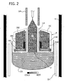
- FIG 2 is a schematic section of another embodiment of the novel crystal puller (with melt heat exchanger (MHE), crystal heat exchanger (CHE), lower heater (LH) and upper heater (UH));
- MHE melt heat exchanger
- CHE crystal heat exchanger
- LH lower heater
- UH upper heater
- Figures 3 and 4 are schematic graphs of defect dynamics
- Figures 5A-5B are comparisons between crystal pullers with and without melt heat exchanger (MHE) using variation in the maximum crucible temperature with the negative melt-side temperature gradient at the melt/crystal interface
- Figure 5A is a graph of maximum crucible temperature comparing the conventional crystal puller to the novel crystal puller
- Figure 5B is a graph substituting heater power for maximum crucible temperature
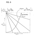
- Figure 6 is a graph showing the relationship between v / G s,f,z and vG l,f,z for different G s,f,z , at the melt/crystal interface;
- Figure 7 is a quantitative graph of variation in parameters at the interface for a fixed vlG s,f,z ;
- Figure 8 is a schematic of a conventional crystal puller, and Figure 8A is a graph of the dependence of crucible temperature on the melt-side temperature gradient at the melt/crystal interface;
- Figure 9 is a graph of the relationship between crucible temperature, and the melt-side temperature gradient at the interface and at the open surface as a function of quality of the crystal puller design
- Figure 10 is a graph of the possible qualitative dependence of the interface shape on melt heat exchanger (MHE) power
- Figure 11 is a graph of radial distribution of G s,f,Z at the interface for a typical crystal puller and for a novel crystal puller with active melt heat exchanger (MHE) and crystal heat exchanger (CHE);
- Figure 12A is a graph showing the comparison between the axial temperature profile in a crystal in the novel crystal puller with active melt heat exchanger (MHE) and crystal heat exchanger (CHE), and that in a conventional crystal puller
- Figure 13 is a graph of the axial temperature profiles in novel crystal pullers with various heat sources and heat sinks operating and a profile of a conventional crystal puller;
- Figure 14 is a graph of the relative variation in G s,f,z versus pull-rate in a conventional crystal puller
- Figure 15 is a simulated temperature field in the base-line conventional crystal puller
- Figure 16A is a graph of axial temperature profile in a growing conventional crystal and Figure 16B is a graph of crystal-side negative axial temperature gradient (G s,f , z ) at the melt/crystal interface as a function of radial location;
- Figure 17 is a simulated temperature field in the heavily insulated novel crystal puller with active upper heater (UH) and inactive melt heat exchanger (MHE), crystal heat exchanger (CHE), and lower heater (LH);
- UH active upper heater
- MHE inactive melt heat exchanger
- CHE crystal heat exchanger
- LH lower heater
- Figure 18A is a graph showing axial temperature profiles in the conventional crystal puller and the insulated novel crystal puller with active upper heater (UH);
- Figure 18B is a graph comparing the conventional crystal puller and the insulated novel crystal puller with active upper heater (UH) with respect to G s,f,z at the interface;
- Figure 18C is a graph of radial variation in the ratio of q fusion,, z / q / i,f,z for the conventional crystal puller and the insulated novel crystal puller with active upper heater (UH);
- Figure 19 is a simulated temperature field in the novel crystal puller with active crystal heat exchanger (CHE) and upper heater (UH) and inactive lower heater (LH) and melt heat exchanger (MHE);
- CHE active crystal heat exchanger
- UH upper heater
- LH inactive lower heater
- MHE melt heat exchanger
- Figure 20A is a graph comparing the conventional crystal puller, the insulated novel crystal puller with active upper heater (UH), and the novel crystal puller with active crystal heat exchanger (CHE) and upper heater (UH) with respect to axial temperature profiles;
- Figure 20B is a graph showing a comparison between the conventional crystal puller, the insulated novel crystal puller with active upper heater (UH), and the novel crystal puller with active crystal heat exchanger (CHE) and upper heater (UH) with respect to G s , f , z ;
- Figure 20C is a graph of variation in the ratio of q fusion,, z / q i,f,z for the conventional crystal puller, the insulated crystal puller with active upper heater (UH), and the novel crystal puller with active crystal heat exchanger (CHE) and upper heater (UH);
- Figure 21 is a simulated temperature field in the novel crystal puller with active crystal heat exchanger (CHE), lower heater (LH), and upper heater (UH) and with inactive melt heat exchanger (MHE);
- CHE active crystal heat exchanger
- LH lower heater
- UH upper heater
- MHE inactive melt heat exchanger
- Figure 22A is a graph comparing the conventional crystal puller, and the various configurations of the novel crystal puller with respect to axial temperature profiles;
- Figure 22B is a graph comparing the conventional crystal puller, and the various configurations of the novel crystal puller with respect to G s,f,z ;
- Figure 22C is a graph of variation in the ratio of q fusion,,z lq i,f,z for the conventional crystal puller and the various configurations of the novel crystal puller;
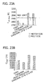
- Figures 23A-23B are bar graphs of maximum crucible temperatures and side heater powers for different configurations of the conventional crystal puller and the novel crystal puller;
- Figures 24A-24B are bar graphs of the relationship between the heat loss from the melt surface (in terms of G l,os,z ) and side heater powers for different configurations of the novel crystal puller;
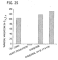
- Figure 25 is a bar graph of radial variation in G s,f,z at the interface for various configurations of the novel crystal puller
- Figure 26 is a simulated temperature field in the novel crystal puller (active melt heat exchanger (MHE), crystal heat exchanger (CHE), lower heater (LH), and upper heater (UH)) at MHE temperature equal to 2100 K and UH power equal to 20kW;
- MHE active melt heat exchanger
- CHE crystal heat exchanger
- LH lower heater
- UH upper heater
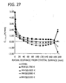
- Figure 27 is a graph of the effect of melt heat exchanger (MHE) temperature on the heat transfer at the open-melt surface for the novel crystal puller (active melt heat exchanger (MHE), crystal heat exchanger (CHE), lower heater (LH), and upper heater (UH));
- MHE melt heat exchanger
- CHE crystal heat exchanger
- LH lower heater
- UH upper heater
- Figure 28 is a graph of the effect of melt heat exchanger (MHE) temperature on the maximum crucible temperature for the novel crystal puller (active melt heat exchanger (MHE), crystal heat exchanger (CHE), lower heater (LH), and upper heater (UH));
- MHE melt heat exchanger
- CHE crystal heat exchanger
- LH lower heater
- UH upper heater
- Figure 29 is a graph of the effect of melt heat exchanger (MHE) temperature on the side heater power in the novel crystal puller (active melt heat exchanger (MHE), crystal heat exchanger (CHE), lower heater (LH), and upper heater (UH));
- MHE melt heat exchanger
- CHE crystal heat exchanger
- LH lower heater
- UH upper heater
- Figure 30 is a graph of the sensitivity of the side heater power to the melt heat exchanger (MHE) temperature in the novel crystal puller (active melt heat exchanger (MHE), crystal heat exchanger (CHE), and lower heater (LH));
- Figures 31A-31D are simulated temperature fields showing dependence of the interface shape on the MHE temperature in the novel crystal puller (active melt heat exchanger (MHE), crystal heat exchanger (CHE), lower heater (LH), and upper heater (UH));
- MHE active melt heat exchanger
- CHE crystal heat exchanger
- LH lower heater
- UH upper heater
- Figure 32 is a graph of the decreasing v / G / ,f,z with increasing melt heat exchanger (MHE) temperature in the novel crystal puller (active melt heat exchanger (MHE), crystal heat exchanger (CHE), lower heater (LH), and upper heater (UH));
- MHE melt heat exchanger
- CHE crystal heat exchanger
- LH lower heater
- UH upper heater
- Figure 33A is a graph of the effect of melt heat exchanger (MHE) temperature on G s,f,z at the interface in a crystal grown in the novel crystal puller (active melt heat exchanger (MHE), crystal heat exchanger (CHE), lower heater (LH), and upper heater (UH));
- MHE melt heat exchanger
- CHE crystal heat exchanger
- LH lower heater
- UH upper heater
- Figure 33B is a graph of the radial variation in G s , f,z in the novel crystal puller (active melt heat exchanger (MHE), crystal heat exchanger (CHE), lower heater (LH), and upper heater (UH));
- MHE active melt heat exchanger
- CHE crystal heat exchanger
- LH lower heater
- UH upper heater
- Figure 33C is a graph of the axial temperature profiles in a crystal grown in the novel crystal puller (active melt heat exchanger (MHE), crystal heat exchanger (CHE), lower heater (LH), and upper heater (UH)) at various MHE temperatures;
- MHE active melt heat exchanger
- CHE crystal heat exchanger
- LH lower heater
- UH upper heater
- Figure 34 is a simulated temperature field in the novel crystal puller (active melt heat exchanger (MHE), crystal heat exchanger (CHE), lower heater (LH), and upper heater (UH)) at MHE power equal to about 27.02 kW;
- MHE active melt heat exchanger
- CHE crystal heat exchanger
- LH lower heater
- UH upper heater
- Figure 35 is a graph of the effect of melt heat exchanger (MHE) power on G l , os,z in the novel crystal puller (active melt heat exchanger (MHE), crystal heat exchanger (CHE), lower heater (LH), and upper heater (UH));
- MHE melt heat exchanger
- CHE crystal heat exchanger
- LH lower heater
- UH upper heater
- Figure 36 is a graph of the effect of melt heat exchanger (MHE) power on the maximum crucible temperature in the novel crystal puller (active melt heat exchanger (MHE), crystal heat exchanger (CHE), lower heater (LH), and upper heater (UH));
- MHE melt heat exchanger
- CHE crystal heat exchanger
- LH lower heater
- UH upper heater
- Figure 37 is a graph of the melt heat exchanger (MHE) power on the side heater power in the novel crystal puller (active melt heat exchanger (MHE), crystal heat exchanger (CHE), lower heater (LH), and upper heater (UH));
- MHE melt heat exchanger
- CHE crystal heat exchanger
- LH lower heater
- UH upper heater
- Figures 38A-38D are simulated variations in the interface shape as a function of the melt heat exchanger (MHE) power in the novel crystal puller (active melt heat exchanger (MHE), crystal heat exchanger (CHE), lower heater (LH), and upper heater (UH));
- MHE melt heat exchanger
- CHE crystal heat exchanger
- LH lower heater
- UH upper heater
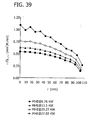
- Figure 39 is a graph of the dependence of G l,f,z on the melt heat exchanger (MHE) power in the novel crystal puller (active melt heat exchanger (MHE), crystal heat exchanger (CHE), lower heater (LH), and upper heater (UH));
- MHE melt heat exchanger
- CHE crystal heat exchanger
- LH lower heater
- UH upper heater
- Figure 40A is a graph of the effect of melt heat exchanger (MHE) power on G s,f,z in the novel crystal puller (active melt heat exchanger (MHE), crystal heat exchanger (CHE), lower heater (LH), and upper heater (UH));
- MHE melt heat exchanger
- CHE crystal heat exchanger
- LH lower heater
- UH upper heater
- Figure 40B is a graph of the effect of melt heat exchanger (MHE) power on the relative uniformity of G s,f,z in the novel crystal puller (active melt heat exchanger (MHE), crystal heat exchanger (CHE), lower heater (LH), and upper heater (UH));
- MHE melt heat exchanger
- CHE crystal heat exchanger
- LH lower heater
- UH upper heater
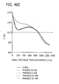
- Figure 40C is a graph of the effect of melt heat exchanger (MHE) power on the time-temperature history of a crystal-segment in the novel crystal puller (active melt heat exchanger (MHE), crystal heat exchanger (CHE), lower heater (LH), and upper heater (UH));
- MHE melt heat exchanger
- CHE crystal heat exchanger
- LH lower heater
- UH upper heater
- Figure 41 is a graph of the effect of melt heat exchanger (MHE) temperature on the maximum crucible temperature in the novel crystal puller (active melt heat exchanger (MHE), crystal heat exchanger (CHE), lower heater (LH), and upper heater (UH));
- MHE melt heat exchanger
- CHE crystal heat exchanger
- LH lower heater
- UH upper heater
- Figure 42A is a graph of the effect of melt heat exchanger (MHE) temperature on G s,f,z (r) in the novel crystal puller (active melt heat exchanger (MHE), crystal heat exchanger (CHE), lower heater (LH), and upper heater (UH));
- MHE melt heat exchanger
- CHE crystal heat exchanger
- LH lower heater
- UH upper heater
- Figure 42B is a graph of the effect of melt heat exchanger (MHE) temperature on the relative uniformity of G s , f,z (r) in the novel crystal puller (active melt heat exchanger (MHE), crystal heat exchanger (CHE), lower heater (LH), and upper heater (UH));
- MHE melt heat exchanger
- CHE crystal heat exchanger
- LH lower heater
- UH upper heater
- Figure 42C is a graph of the effect of melt heat exchanger (MHE) temperature on the time-temperature history of a crystal-segment in the novel crystal puller (active melt heat exchanger (MHE), crystal heat exchanger (CHE), lower heater (LH), and upper heater (UH));
- MHE melt heat exchanger
- CHE crystal heat exchanger
- LH lower heater
- UH upper heater
- Figure 43 is a graph of the effect of pull-rate on the heat transport between MHE and melt in the novel crystal puller (active melt heat exchanger (MHE), crystal heat exchanger (CHE), lower heater (LH), and upper heater (UH));
- MHE active melt heat exchanger
- CHE crystal heat exchanger
- LH lower heater
- UH upper heater
- Figure 44 is a graph of the effect of pull-rate on the side heater power in the novel crystal puller (active melt heat exchanger (MHE), crystal heat exchanger (CHE), lower heater (LH), and upper heater (UH)), the MHE temperature is fixed at 1900K, the LH and UH powers are fixed at 2.28 kW and at 20kW, respectively;
- MHE active melt heat exchanger
- CHE crystal heat exchanger
- LH lower heater
- UH upper heater
- Figure 45 is a graph of the effect of increasing pull-rate on the maximum crucible temperature in the novel crystal puller (active melt heat exchanger (MHE), crystal heat exchanger (CHE), lower heater (LH), and upper heater (UH)), the MHE temperature fixed at 1900 K;
- MHE active melt heat exchanger
- CHE crystal heat exchanger
- LH lower heater
- UH upper heater
- Figure 46 is a graph of the effect of pull-rate on the melt-side axial temperature gradients in the novel crystal puller (active melt heat exchanger (MHE), crystal heat exchanger (CHE), lower heater (LH), and upper heater (UH)), the MHE temperature fixed at 1900 K;
- MHE active melt heat exchanger
- CHE crystal heat exchanger
- LH lower heater
- UH upper heater
- Figure 47 is a graph of the increasing contribution of heat generated by solidification with increasing pull-rate in the novel crystal puller (active melt heat exchanger (MHE), crystal heat exchanger (CHE), lower heater (LH), and upper heater (UH));
- MHE active melt heat exchanger
- CHE crystal heat exchanger
- LH lower heater
- UH upper heater
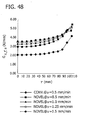
- Figure 48 is a graph of the effect of pull-rate on the uniformity and magnitude of G s,f,z (r) in the novel crystal puller (active melt heat exchanger (MHE), crystal heat exchanger (CHE), lower heater (LH), and upper heater (UH));
- MHE active melt heat exchanger
- CHE crystal heat exchanger
- LH lower heater
- UH upper heater
- Figure 49 is a graph of the relative variation in G s,f,z as a function of pull-rate in the novel crystal puller (active melt heat exchanger (MHE), crystal heat exchanger (CHE), lower heater (LH), and upper heater (UH));
- MHE active melt heat exchanger
- CHE crystal heat exchanger
- LH lower heater
- UH upper heater
- Figure 50 is a graph of the non-linear relationship between v and v / G s,f,z in the novel crystal puller (active melt heat exchanger (MHE), crystal heat exchanger (CHE), lower heater (LH), and upper heater (UH));
- MHE active melt heat exchanger
- CHE crystal heat exchanger
- LH lower heater
- UH upper heater
- Figure 51 is a graph of the quasi-steady state temperature profiles in a crystal growing in the novel crystal puller (active melt heat exchanger (MHE), crystal heat exchanger (CHE), lower heater (LH), and upper heater (UH)) as a function of the pull-rate;
- MHE active melt heat exchanger
- CHE crystal heat exchanger
- LH lower heater
- UH upper heater
- Figures 52A-52D are simulated interface shapes as a function of the pull-rate in the novel crystal puller with active melt heat exchanger (MHE), crystal heat exchanger (CHE), lower heater (LH), and upper heater (UH), the MHE temperature fixed at 1900 K;
- MHE active melt heat exchanger
- CHE crystal heat exchanger
- LH lower heater
- UH upper heater
- Figure 53A is a simulated temperature field in the novel crystal puller with active melt heat exchanger (MHE) and crystal heat exchanger (CHE) at the pull-rate equal to 0.5 mm/min., the MHE power fixed at 40.53 kW and the CHE temperature fixed at 300 K;
- MHE active melt heat exchanger
- CHE crystal heat exchanger
- Figure 53B is a simulated temperature field in the novel crystal puller with active melt heat exchanger (MHE) and crystal heat exchanger (CHE) at the pull-rate equal to 2.5 mm/min.;
- Figure 54 is a graph of the radial variation in the melt-side negative axial temperature gradient at the open surface with the pull-rate for the novel crystal puller with active melt heat exchanger (MHE) and crystal heat exchanger (CHE);
- Figure 55 is a graph of the side heater power as a function of the pull-rate in the novel crystal puller with active melt heat exchanger (MHE) and crystal heat exchanger (CHE);
- Figure 56 is a graph of the decreasing maximum crucible temperature with increasing pull-rate in the novel crystal puller with active melt heat exchanger (MHE) and crystal heat exchanger (CHE);
- Figure 57 is a graph of the radial variation of G s,f,z as a function of the pull-rate in the novel crystal puller with active melt heat exchanger (MHE) and crystal heat exchanger (CHE);
- Figure 58 is a graph of the relative radial variation of G s,f,z with increasing pull-rates in the novel crystal puller with active melt heat exchanger (MHE) and crystal heat exchanger (CHE);
- Figure 59 is a graph of the relative effect of increasing contribution of the heat generated by solidification to the conductive heat transfer in the crystal (measured in terms of v / G / ,f,z ) with increasing pull-rate in the novel crystal puller with active melt heat exchanger (MHE) and crystal heat exchanger (CHE);
- Figures 60A-60C are simulated interface shapes as a function of the pull-rate in the novel crystal puller with active melt heat exchanger (MHE) and crystal heat exchanger (CHE);
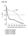
- Figure 61 is a graph of the axial temperature profile in a growing crystal in the novel crystal puller with active melt heat exchanger (MHE) and crystal heat exchanger (CHE); and
- Figure 62 is a graph of vlG s,f,z as a function of the pull-rate in the novel crystal puller with active melt heat exchanger (MHE) and crystal heat exchanger (CHE).
- MHE active melt heat exchanger
- CHE crystal heat exchanger
- an embodiment of the novel crystal puller CP comprises a housing H and a quartz crucible CR in the housing for containing a semiconductor material (e.g., silicon) melt M.
- a pulling mechanism P (suitably a shaft or pull wire) secured in the housing and adapted to extend toward the crucible is adapted to continuously pull the solid monocrystalline ingot or crystal C from the melt.
- a tubular graphite reflector R (or heat shield) suitably secured in a growth chamber of the housing H includes a cover GC suitably made of graphite and having a central opening sized and shaped for surrounding the growing crystal.
- An annular melt heat exchanger MHE is mounted within the cover GC to face the exposed melt surface MS.
- the melt heat exchanger MHE includes a heat source, such as an electrically-powered heater.
- the melt heat exchanger MHE may also include heat absorption structure.
- a crystal heat exchanger CHE (or active cooling jacket) is also mounted within the cover GC to surround and to face the growing crystal C.
- the crystal heat exchanger CHE is disposed above the melt heat exchanger MHE as close to the melt/crystal interface F as practical, desirably such that the crystal heat exchanger CHE cools (or removes heat from) a crystal segment proximate the interface.
- the crystal heat exchanger CHE is cooled by conventional cooling fluid (typically water), though other heat transfer media may be used.
- the crystal heat exchanger CHE may also include a heater.
- the temperature (and resulting heat transfer capacity) of the melt heat exchanger is controlled by regulating the electrical current (the power) passing therethrough.
- the temperature of the crystal heat exchanger is suitably controlled by regulating the temperature and flow rate of the cooling fluid.
- the cover GC of the reflector R may also be filled, or at least partially filled, with insulation INS, for example to resist radiative heat transfer between the exposed melt surface MS (the exposed upper surface portion of the melt) and the crystal outer surface.
- Insulation INS of appropriate thermal conductivity may optionally be disposed between the melt heat exchanger MHE and the open melt-surface MS to further control (e.g., inhibit) heat transfer between the melt-surface and the MHE.
- insulation INS of desired thermal conductivity is disposed between the crystal heat exchanger CHE and the crystal C. Note that in addition to, or instead of, manipulating the temperature of the melt heat exchanger MHE and crystal heat exchanger CHE, the thermal conductivity of the insulation INS can be appropriately selected to control heat transfer.
- the thermal conductivity, thickness and material of the insulation INS can be selected to correspond to the heat transfer desired.
- the melt heat exchanger MHE may be constructed to have a controllable radial and/or axial power profile, and the crystal heat exchanger CHE may similarly be constructed to have controllable axial and/or radial cooling profile.
- the reflector R therein is significantly thicker than conventional reflectors.
- the reflector R has a relatively constant inner and outer diameter over most of its height, resuming in a reflector thickness of at least 200 mm, 300 mm, 400 mm, or in some embodiments, at least 500 mm. A substantial portion of the insulation is of nearly the same thickness as the reflector R.
- Heat loss from the exposed melt surface MS is actively controlled by operation of the melt heat exchanger MHE to increase the G l,f,z (negative melt-side temperature gradient at the interface) without significantly increasing the crucible temperature T cr .
- Actively changing the effective temperature of the environment above the exposed melt surface MS i.e., the environment that the melt'sees', more effectively controls the heat loss from the melt-surface than prior art passive shields and reflectors. There is no active control over the effective temperature if the melt surface is merely covered by the prior art reflecting and insulating material.
- the active heat source in this embodiment disposed in the melt heat exchanger MHE.
- the active heat source of the melt heat exchanger MHE may be sized to cover or face as much of the melt surface as practical.
- the heat source has an area sized at least 30%, more preferably at least 40%, even more preferably at least 50%, more preferably at least 60%, and even more preferably at least 75% of an area of the exposed melt surface MS (the exposed upper surface portion). Note that the relevant area of the exposed melt surface MS does not include the portion occupied by the crystal C.
- the heat source is disposed opposite the melt surface and in one embodiment, the heat source extends generally parallel to the melt surface. Note that the heat source, or portions thereof may be angled relative to the melt surface within the scope of this invention.
- the heat source in particular a lower surface of the heat source, is adapted to be disposed proximate the melt surface, for example, within 100 mm, 50 mm and in some embodiments within 30mm thereof.
- the space between the melt heat exchanger MHE heat source and the exposed melt surface MS may vary as the melt M is consumed.
- the crucible CR is typically moved upward by suitable means during crystal growth so as to reduce such variation of the distance, though it is contemplated to move the reflector R or components therein as well.
- the structural components of the crystal puller CP need not be removed or added to the puller to produce a desired product. However, each component need not necessarily be active or operating during crystal growth.
- Operation of the melt heat exchanger MHE tends to decrease the heat loss from the open melt surface MS but tends to increase the heat transfer to the crystal surface, thereby increasing the crystal temperature and decreasing the G s , f,z (crystal side negative temperature gradient at the melt/crystal interface). Such an increase may cause a reduction in pull rate and thereby reduce productivity. Operation of the crystal heat exchanger CHE should compensate for the effect of the melt heat exchanger MHE and serve to increase G s,f,z . Depending upon the cooling capacity of the crystal heat exchanger CHE, the increase in G s,f,z can be relatively high, which can improve the productivity significantly.
- the heat transfer path between the melt heat exchanger MHE and the crystal heat exchanger CHE is insulated to allow relatively independent tuning (control) of both the MHE and the CHE.
- the benefits of the crystal heat exchanger CHE i.e., the cooling effect
- the crystal heat exchanger CHE i.e., the cooling effect
- FIG. 5A The variation in crucible temperature as a function of melt-side temperature gradients in the novel crystal puller CP compared to a traditional crystal puller is shown qualitatively in Figure 5A .
- Figure 5B shows the side heater power for similar crystal pullers.
- Significant factors in achieving a desired microdefect distribution in a crystal-segment include controlling v / G s,f,z at the melt/crystal interface F, the radial variation of vlG s,f,z and the time-temperature or thermal history of the segment.
- Crystal growth is a dynamic process.
- Equation (1) states that sum of the conductive heat on the melt-side and the heat generated by solidification is transferred by conduction through the crystal C. This balance assumes that crystal C, even at high temperatures, does not act as a heat-pipe and that the mode of heat transfer through the crystal is conduction.
- Equation (3) states that for a given G s,f,z , maximum pull-rate can be achieved when the melt-side temperature gradient at the interface, G l , f,z , is equal to zero.
- the melt M should be isothermal for the pull-rate to be maximum for a given crystal-side temperature gradient.
- (vlG s,f,z ) mx is generally a function of material properties, and for silicon, its value is between 0.5 and 1. Width of this range is determined by the variation in reported values for the heat of fusion for silicon.
- Equation (3) has infinite solutions for a given v / G s,f,z at the interface, which means that there are infinite variations in the crystal puller design that allow crystal growth at a given v / G s,f,z with varying G l,f,z at the interface.
- the solutions can be plotted on a vlG s,f,z vs. G l,f,z graph. Points of constant G s,f,z are connected to show a family of constant G s,f,z lines. Each line represents a straight line given by equation (3) for a fixed G s,f,z .
- each line represents (vlG s,f,z ) mx and the slope is equal to - ⁇ l ⁇ s ⁇ - ⁇ ⁇ H ⁇ G s , f , z .
- the slope of the line decreases the temperature gradient increases.
- Pull-rates change along constant G s , f,z lines. Movement towards intersection of a constant G s,f,z line and the v / G s,f,z axis indicates increasing pull-rates and movement away from this intersection indicates decreasing pull-rates. It is obvious that changing pull-rates in this way changes v / G s,f,z ratio. Therefore, pull-rate or the productivity of a defect-controlled crystal cannot be increased in this manner.
- the novel crystal puller CP enables higher pull-rates for a given vlG s,f,z ratio than a conventional crystal puller due to manipulation of the dynamics between some parameters.
- the novel crystal puller CP enables a much greater change in the melt-side temperature gradient at the interface relative to the change in the crucible temperature. In this way, very high melt-side temperature gradients at the interface can be achieved while maintaining the crucible CR below maximum allowable crucible temperature, T cr,mx .
- the ratio of change in the melt-side temperature gradient at the interface (G l , f,z as well as the average gradient) to the change in the crucible temperature is increased in the new crystal puller.
- Figure 9 shows the relationship between the ratio and quality (unitless) of the crystal puller design. As the relationship between the crucible temperature and the melt-side temperature gradient at the interface becomes more efficient, the pull-rate of the crystal C, and hence, the productivity can be increased.
- the melt M becomes hotter and the heat loss from the exposed melt surface MS increases.
- the heat loss may be measured by an increase in the heat flux normal to the open melt surface MS i.e., by the melt-side temperature gradient at the MS.
- the negative melt-side temperature gradient at the open or exposed melt surface is denoted by G l,ms,z .
- Subscript ms denotes the exposed melt surface MS.
- the crucible temperature is interactively set by manipulating the side heater power to establish a condition at the melt/crystal interface F that satisfies equation (1) (or in 1-dimensional sense, equation (2)).
- heat entering the crystal C from the melt M is quite negligible compared to the total heat loss from the open melt surface MS.
- a quasi-steady-state heat balance indicates that as the heat loss from the open melt surface MS increases the heat entering the melt M from the side heater (through the side of the crucible) increases. In essence, the balance results in an increase in side heater power and the crucible temperature.
- heat loss from the melt surface MS is desirably decreased to control or limit the increase in the crucible temperature.
- the ratio of change in the axial melt-side temperature gradient at the exposed melt surface MS to the change in the crucible temperature should be low (see Figure 9 ).
- equation (6) states that as the heat loss from the open melt surface MS decreases, less heater power is required to grow the crystal C and the increase in crucible temperature is correspondingly reduced.
- the initial point defect incorporation in a growing crystal depends, at least in part, on (v / G s,f,z ).
- the shape of the interface tends to be curvilinear. Therefore, the effect of temperature gradients at the (curvilinear) meltlcrystal interface F should be addressed to understand the point defect incorporation.
- the radial uniformity in the incorporated point defect field depends, at least in part, on the interface shape:
- process tuning e.g., control of the melt heat exchanger, crystal heat exchanger, among other components
- G s,f,z ( r ) is desirable to achieve desired G s,f,z ( r ) .
- equation (1) is applied for an axi-symmetric two-dimensional model of the crystal puller.
- Subscript r and z indicate r and z directions.
- Subscript fusion indicates the heat-flux by solidification of melt and subscript n indicates normal flux. Note that when n is not used as a subscript, it denotes the unit vector normal to the interface. It is evident that as the radial uniformity of the flux ( q s,f,z ) increases, the radial uniformity of the gradient ( G s , f , z ) increases. The same argument holds true for the melt-side.
- the novel crystal puller CP may be controlled or tuned to vary the local temperature field at or near the melt/crystal interface F such that a desired predetermined gradient ( G s,f , z ( r )) is achieved.
- the novel crystal puller CP is capable of manipulating and tuning (or controlling) the shape of the interface such that the optimum radial control of G s,f,z is achieved, and to allow an efficient growth process.
- the capacity of the crystal puller to manipulate and tune the interface shape, e.g., for a fixed pull-rate enables a process that produces defect-controlled silicon, among other types of crystal.
- the shape of the melt/crystal interface F changes as a function of the temperature field at or near the interface (the local temperature field). Most of the heat entering the melt is transferred through the exposed melt surface MS to the environment. Thus, controlling the heat transfer through the open melt surface MS using, e.g., the melt heat exchanger MHE heat source, effectively changes the temperature field in the melt M and the crystal C (and thus the local temperature field).
- the local temperature field typically affects initial type and concentration of intrinsic point defects as the silicon solidifies.
- the local temperature field generally ranges from the temperature of solidification (i.e., about 1410°C) to a temperature greater than about 1300°C (i.e., about 1325°C, 1350°C or more).
- the active melt heat exchanger MHE can also change the global temperature field (the field away from the interface).
- the temperature of the melt heat exchanger MHE influences the magnitude and the direction of the heat flux from the melt-surface. Note that the temperature of the melt heat exchanger MHE can be manipulated by controlling the current passing through it (the power). As the melt heat exchanger MHE power (and therefore temperature) increase, the heat loss from the melt-surface decreases. Operating the melt heat exchanger MHE, even at relatively low power temperature, tends to enable a decrease in the side heater temperature. Generally, as the melt heat exchanger MHE power increases, the required side heater power decreases.
- melt heat exchanger MHE causes the melt/crystal interface F to move downward.
- the downward movement of the interface can also be facilitated by operation of the crystal heat exchanger CHE.
- the shape of the melt/crystal interface F can be manipulated and controlled. Manipulation of the interface shape helps to control the radial variation and uniformity of the axial heat flux into the crystal C.
- a qualitative graph of variations in the interface shape as a function of increasing melt heat exchanger MHE power is shown in Figure 10 .
- the melt heat exchanger MHE and the crystal heat exchanger CHE may be used to maintain a relatively high gradient (G s,f,z ) at the interface.
- the melt heat exchanger MHE is desirably operated to maintain satisfactory control of the gradient (G s,f,z (r)).
- the novel crystal puller CP enables relatively high productivity (relatively high pull rate) and control of G s,f,z ( r ) at the interface.
- a comparison between the radial variation of gradient (G s,f,z ) at the interface for the novel crystal puller CP and that a conventional crystal puller is shown in Figure 11 .
- the novel crystal puller CP performs far better than conventional crystal pullers.
- melt heat exchanger MHE Operation of the melt heat exchanger MHE tends to decrease the overall temperature of the melt M.
- the melt M also becomes more isothermal and thereby promotes uniform axial temperature gradients on the melt-side at the melt/crystal interface F.
- the melt heat exchanger MHE in conjunction with the side heater, forms a distributed heat source to improve the radial uniformity.
- the novel crystal puller CP enables control of radial uniformity and variation in v / G s,f,z at the interface and limits the temperature of the crucible CR.
- Melt heat exchanger MHE power should remain relatively low to moderate. As the melt heat exchanger MHE power temperature increases significantly, the melt M can become very hot and the interface may start moving upward away from the M. But even if the melt M becomes very hot, manipulation of the melt heat exchanger MHE power can still be used to tune or control the interface shape and radial variation of G s,f,r ( r ).
- the growth conditions at the melt/crystal interface F for a given crystal C section or segment affect initial point defect incorporation in the segment.
- subsequent defect dynamics is a function of the thermal history of the crystal segment.
- the temperature field in the crystal C changes as it grows.
- the temperature does not change significantly even as the crystal C grows.
- all crystal segments may be assumed to traverse through the same temperature field.
- the time-temperature path of a crystal-segment is obtained by knowing the history of pull-rate as a function of time and the temperature field.
- the novel crystal puller CP can satisfactorily manufacture, for example, any rapid cooled silicon RCS product.
- the axial temperature profile of a crystal C grown in the Figure 1 embodiment is given by Figure 12A , qualitatively.
- Figure 12A also compares the axial temperature profile in a crystal C in a typical conventional crystal puller with that in the crystal grown with active melt heat exchanger MHE and crystal heat exchanger CHE in the novel puller.
- the temperature drop in the C in the novel crystal puller CP with active melt heat exchanger MHE and crystal heat exchanger CHE occurs at much higher rates very close to the melt/crystal interface F.
- the local cooling rates of crystal segments given by the product of pull-rate and the negative axial temperature gradient ( vG s,z ) are much higher for the novel crystal puller CP.
- nucleation temperature is determined by the maximum in the nucleation rate versus temperature curve. If the cooling rates through nucleation temperature are very high, only insignificant nucleation typically takes place. Thus, nucleation temperature in Figures 12A and 12B indicates only the theoretical maximum in nucleation rate but not the number of nuclei formed. In a rapid cooled silicon RCS product, number of microdefects can be very low, although all crystal-segments traverse through a maximum in the nucleation rate.
- the gradient G s,f,z at the interface for the novel crystal puller CP can be controlled more efficiently than for a prior art crystal puller. Therefore, practically all rapid cooled silicon RCS products can be produced in the novel crystal puller CP shown in Figure 1 .
- novel crystal puller CP of Figure 1 mainly addresses the control and manipulation of interfacial conditions. Therefore, additional components (e.g., heaters) are desirably added to the design, as described with respect to Figure 2 , to manipulate and control the time-temperature path of a given crystal segment.
- additional components e.g., heaters
- Some crystal types are manufactured by growing the entire or significant part of the crystal C above the nucleation range of the relevant point defect species, followed by rapid cooling of the crystal in a cooling chamber. Also, manufacture of some crystal relies on allowing extended residence time for crystal-segments through the high temperature zone before nucleation rates of point defects reach their maximum values. Since the residence time is marked by significant diffusion of point defects, it is often termed the "diffusion time.”
- the axial temperature drop in the crystal growing in the novel-crystal puller with only active melt heat exchanger MHE and crystal heat exchanger CHE is relatively high. In other words, crystal segments spaced or distant from the melt/crystal interface F may cool too quickly. Therefore, some modifications to the novel crystal puller CP may be made to maintain a higher temperature or slow the cooling in such crystal segments.
- the novel crystal puller CP of the second embodiment generally allows growth of the crystal C above a set temperature and extends the diffusion time.
- the second embodiment contains the components of the previous embodiment, including the reflector R, melt heat exchanger MHE and the crystal heat exchanger CHE.
- a tubular lower crystal heater LH and tubular upper heater UH are included.
- the lower heater LH is disposed inside the cover GC and above the crystal heat exchanger CHE for maintaining the crystal temperature above the required nucleation temperature range. As shown, there is little or no space between the crystal heat exchanger CHE and the lower heater LH, though it is contemplated to space the lower heater from the crystal heat exchanger.
- the lower crystal heater LH is suitably electrically heated, substantially similar to the melt heat exchanger MHE, and its power is controlled by regulating the current passing therethrough.
- the lower and upper heaters (LH and UH) may be constructed to have a controllable axial power profile, and the melt heat exchanger MHE may be constructed to have a controllable radial and/or axial power profile, and the crystal heat exchanger CHE may similarly be constructed to have controllable axial and/or radial cooling profile, as noted above.
- the lower heater LH profile and temperature typically depends on the cooling provided by the crystal heat exchanger CHE and the targeted nucleation temperature range.
- Heat provided by the lower heater LH can keep the crystal segments that are distant from the interface warmer for an extended period of time, allowing the extended diffusion and interaction time for point defects and other impurities.
- some crystal types rely on extended diffusion time for point defect diffusion and annihilation followed by rapid quenching through the nucleation temperature.
- the extended diffusion and rapid quenching is accomplished by growing the entire crystal below nucleation temperature and then transferring it to an optional cooling chamber (not shown) located inside the crystal puller. The distance between the melt/crystal interface F and the axial location of the relevant nucleation temperature determines the length of the diffusion time-dependent crystal.
- the upper heater UH is disposed above the lower heater LH.
- the upper heater UH may be used for distributed axial heating over an extended length of the growing crystal, such as for extended diffusion.
- the upper heater UH is suitably disposed above and outside the reflector R and spaced significantly from the lower heater LH.
- a cooling chamber (not shown) may be disposed above the upper heater UH to allow rapid quenching after growth, such as under conditions of extended diffusion and interaction.
- the structural components need not be removed or added to the puller to produce a desired product. However, each component need not necessarily be operating during crystal growth.
- Figure 13 with active (operating) melt heat exchanger MHE, crystal heat exchanger CHE, lower heater LH and upper heater UH, a desirable relatively flat axial temperature profile exists in the crystal C.
- Figure 13 also compares the temperature profiles in growing crystals C in the novel crystal puller CP with operating melt heat exchanger MHE and crystal heat exchanger CHE, and a conventional crystal puller.
- the novel crystal puller CP with active melt heat exchanger MHE, crystal heat exchanger CHE, lower heater LH and upper heater UH the radial profile and the magnitude of G s,f,z at the interface also remain comparable to those in the first embodiment ( Figure 11 ).
- the novel crystal puller CP with melt heat exchanger MHE, crystal heat exchanger CHE, lower heater LH and upper heater UH is versatile and can create different temperature fields in the crystal puller necessary for growing a variety of crystal types.
- the several heat sources (melt heat exchanger MHE, lower heater LH, upper heater UH) and the heat sink (crystal heat exchanger CHE) can be turned on or off depending on the desired temperature field.
- the magnitude and power profile of the heaters (melt heat exchanger MHE, lower heater LH, upper heater UH), and magnitude and axial profile of cooling capacity of the crystal heat exchanger CHE can be manipulated.
- the second embodiment crystal puller can generate temperature fields similar to the first embodiment by switching off lower and upper heaters (LH and UH). Many different crystal types can be produced using the novel crystal puller CP.
- novel crystal puller CP Modes of the operation of the novel crystal puller CP are identified below by the active heat sources (heaters) and heat sink (crystal heat exchanger CHE).
- active heat sources heat sources
- heat sink crystal heat exchanger CHE
- novel crystal puller CP with active melt heat exchanger MHE and upper heater UH means that the CP operates with active MHE and UH while crystal heat exchanger CHE and lower heater LH are switched off.
- operations of the novel crystal puller CP are distinguished by specifying active heat sources and sinks while the crystal puller itself is generically referred to as the CP.
- the novel crystal puller CP may be verified by performing various numerical experiments. The study was accomplished by comparing the performance of the novel crystal puller CP with a conventional crystal puller. The numerical experiments are accomplished, for example, by simulating the temperature field for the novel crystal puller CP and analyzing the results.
- An acceptable quantitative model describing the crystal growth is used for numerical simulation of the growth process in the novel crystal puller CP.
- An acceptable model for crystal-growth includes momentum balance in the melt M and atmosphere, and an energy balance in all components of the crystal puller.
- Argon atmosphere is the typical atmosphere for crystal growth.
- Energy balances in each phase are coupled by boundary conditions defined by conduction, radiation and convection. System equations formed by momentum and energy balance can be a difficult to solve for turbulent flow involving radiative heat transfer. As the crucible CR size increases the buoyancy driven melt-flow becomes turbulent. This is true for practically all of today's crystal pullers.
- a direct numerical simulation of the system involving many solid and fluid phases exchanging energy by all modes of energy transfer, where a fluid exhibits turbulent flow can become very expensive and impractical. Therefore, an acceptable model used for the numerical simulation herein involves reasonable assumptions. In this study we use a popular model used by Virzi. The following assumptions are made:
- the thermal history of a crystal segment can be obtained by generating the steady state temperature field in a crystal at various lengths. Further simplification can be made by assuming that all segments of a crystal pass through a temperature field fixed in r and z. This fixed temperature field can be computed once, for a long crystal, e.g., greater than 800 mm. Thus, the problem becomes simpler by fixing the temperature field independent of the crystal-length. However, it is not necessary to assume that the crystal temperature field is independent of the crystal length. Several pseudo-steady state temperature fields describing different crystal lengths can be simulated and the thermal history of a crystal segment can be computed by interpolation between these temperature fields.
- T T coolant
- T s ⁇ lg T m where subscript s/g denotes the tri-junction node.
- the tri-junction node defines the intersection of the melt/crystal interface F with the outer crystal-surface. The spatial location of the tri-junction node is fixed.
- melt/crystal interface F defined by the isotherm at the melting temperature is anchored at the tri-junction ,node.
- energy balance across the melt/crystal interface F is given by the balance between the sum of conductive heat flux from the melt-side and the heat generation rate by fusion per unit area, and the total conductive flux into the crystal across the interface.
- the temperature field inside the crystal puller is predicted by simultaneous solution of equations (10) through (16) and equation (1).
- the interface shape is given by the isotherm at the melting point anchored at the tri-junction node.
- the typical design of the conventional crystal puller and its temperature field are shown in Figure 15 .
- the temperature field in the crystal pullers is simulated using a commercially available finite-element based Software (MARC).
- MMC finite-element based Software
- the conventional crystal puller in this study is the one that defines the upper limit in productivity of defect-controlled crystal.
- the conventional crystal puller is well-insulated.
- the passive reflector no active heating or cooling
- the upper heater upper heat exchanger
- UH keeps the crystal warmer such that the axial location of the relevant nucleation temperature, (in this case, nucleation temperature for self-interstitials, 1173 K) is around 900 mm above the meltlcrystal interface F.
- the axial temperature profile in a relatively long crystal grown using the conventional crystal puller is shown in Figure 16A .
- the corresponding radial variation of the negative axial crystal-side temperature gradients at the interface (G s,f,z ) is shown in Figure 16B .
- FIG 17 shows the temperature field in the heavily insulated novel crystal puller CP.
- Figure 18A shows that the heavily insulated novel crystal puller CP keeps a 900 mm long crystal above the nucleation temperature of self-interstitials. It can be seen that the radial, variation in G s,f,z for the heavily insulated novel crystal puller CP is greatly minimized ( Figure 18B ).
- the absolute value of G s,f,z is very low as a result of increased conduction path.
- the ratio of rate of heat generation by solidification to the rate of axial heat transfer from the melt M is relatively'high. This ratio can be represented by v / G l,f,z (or vlG s,f,z ) at various radial locations.
- Figure 18C shows radial variation of this ratio for the insulated crystal puller and conventional crystal puller.
- Figure 18C should not be used for direct comparison between conventional and the heavily insulated novel crystal puller CP.
- the upper heater UH helps to maintain the crystal C above the targeted nucleation temperature. Therefore, the upper heater UH is active (operates) for all simulations herein unless otherwise specified.
- FIG 19 shows the temperature field in the crystal C grown in the novel crystal puller CP with active crystal heat exchanger CHE and upper heater UH.
- Figures 20A and 20B display axial temperature profile and radial variation of G s,f,z , respectively.
- the crystal C is rapidly cooled in the presence of an active crystal heat exchanger CHE so that in-situ cooling rates around the nucleation temperature can be very high. Pull-rates around 1.1 mm/min, for a target v / G s,f,z (at the interface) equal to 0.134 K.mm 2 /s can be achieved.
- the radial variation in G s,f,z at the interface is quite significant and a length of the crystal C below nucleation temperature may be reduced to less than 150 mm.
- the ratio vlG l,f,z is very low for this configuration ( Figure 20C ).
- the variation in G s,f,z can result in significant variation in the incorporated point defect concentration.
- the pre-nucleation diffusion-time allowed for a particular crystal-segment to reduce the point defect concentration is also very low as a result of the steep axial temperature profile.
- the variation may require very high in-situ cooling rates around the nucleation temperature to quench or control the microdefect formation. In many cases, such in-situ cooling rates are not achieved. Therefore, a practical solution for making a defect sensitive crystal for such radial variation in v / G s,f,z may involve increasing the pre-nucleation diffusion and annihilation time for point defects by activating the lower heater LH.
- FIG 21 The temperature field in the novel crystal puller CP with active crystal heat exchanger CHE and lower heater LH is shown in Figure 21 .
- Figure 22A shows the effect of lower heater LH on the axial temperature profile.
- the length of the crystal C above the interstitial-nucleation temperature is again around 900 mm.
- Steep axial temperature gradients ( Figure 22B ) may allow relatively high pull-rates, e.g., around 1 mm/min, at critical v/G s,f,z .
- this active crystal heat exchanger CHE and lower heater LH configuration may still suffer from radial variation in v / G s,f,z .
- Figure 22C the contribution of heat of fusion to G s,f,z is quite low compared to the contribution of melt-side conduction, which will be addressed below.
- FIGS 23A-B show the maximum crucible temperatures T cr, mx and the side heater power Q sh for various configurations. As shown, side heater power ranges from about 80 KJ/s to about 160 KJ/s, though the power may range to as low as 40, or even as low as 0 KJ/s, within the scope of the invention.
- FIG. 26 shows the temperature field in the novel crystal puller CP with active melt heat exchanger MHE, crystal heat exchanger CHE (fixed at about 300°K), lower heater LH (fixed at about 17.6 kW) and upper heater UH (fixed at about 20 kW (UH is fixed at 20 kW for all simulations unless otherwise noted)) for a fixed MHE temperature of about 2100°K.
- the effect of varying melt heat exchanger MHE temperature on G /,os,z is shown in Figure 27 .
- melt heat exchanger MHE temperature does not dominate enough to increase the melt-side crucible temperature levels to the inoperable regime.
- the melt-side crucible temperatures tend to be mainly affected by the combination of the melt heat exchanger MHE temperature and side heater power, and hence, do not vary much.
- the melt-side temperatures are desirably lower than the maximum allowable temperature, and thus, do not pose any problems for crystal C growth.
- increasing the melt heat exchanger MHE temperature enables reduction, e.g., simultaneous reduction, of the side heater power (Q SH ).
- melt heat exchanger MHE temperature is also increased so as to decrease the crucible CR temperature during crystal C growth. Care should be taken not to increase the melt heat exchanger MHE temperature beyond the maximum allowable temperature at which melt-side crucible temperatures become too high for most practical operations.
- Figures 31A-D show the change in the interface shape with increasing melt heat exchanger MHE temperature, the lower heater LH power being fixed at about 17.6 kW, the crystal heat exchanger CHE temperature fixed at about 300°K and the upper heater UH power fixed at 20 kW.
- the side heater power required to maintain the melt M at temperature decreases.
- the melt crystal interface moves downward to cause an increase in the radial heat flux in the crystal C closer to the surface, but without significantly increasing the axial flux.
- the radial uniformity of the melt-side axial heat-flux improves with increasing melt heat exchanger MHE temperature.
- the radial uniformity or the variation of G s,f,z is controlled by controlling the interface shape.
- the axial heat-flux from the melt M into the crystal C decreases.
- Figure 32 shows decreasing contribution of the axial heat-flux vlG l,f,z from the melt-side with increasing melt heat exchanger MHE temperature.
- the radial uniformity of the melt-side axial heat-flux improves with increasing melt heat exchanger MHE temperature, which increases the ratio of the heat flux by fusion to the melt-side axial heat flux and contributes to the improvement in the radial uniformity of G s,f,z .
- Figure 33A compares the effect of changing melt heat exchanger MHE temperatures on G s,f,z . Note that there is some heat leak from melt heat exchanger MHE to the crystal C. However, the net effect is that the radial uniformity and magnitude of G s,f,z (r) in the crystal C increase ( Figure 33B ). Increasing melt heat exchanger MHE temperature compensates for the radial non-uniformity which tends to be introduced by the crystal heat exchanger CHE.
- melt heat exchanger MHE temperature is at least about 1950°K
- the radial uniformity of G s,f,z for the novel crystal puller CP with active (operating) melt heat exchanger MHE, crystal heat exchanger CHE, lower heater LH and upper heater UH is better than it is for the conventional putter.
- Use of this novel crystal puller CP also allows higher G and therefore allows higher pull-rates at the same or similar v / G s,f,z ,.
- the axial temperature profiles in a crystal C as a function of changing melt heat exchanger MHE temperatures are shown in Figure 33C .
- One of the objectives of designing the novel crystal puller CP is to control the thermal history of crystal segments irrespective of the MHE effect.
- the melt heat exchanger MHE temperature tends to have a minor effect on the thermal history.
- Manipulating the melt heat exchanger MHE power can also change the effective temperature of the environment of the melt-surface. In fact, in practice it is much easier to control power than the temperature. Therefore, in the following sections some of the examples based on varying the effective melt heat exchanger MHE power are discussed.
- novel crystal puller CP with active melt heat exchanger MHE, crystal heat exchanger CHE, lower heater LH and upper heater UH enables maintenance of vlG s,f,z (r) closer to its critical value while providing sufficient diffusion and annihilation time for point defects before significant nucleation (broadly, formation and growth) of the relevant species takes place.
- the novel crystal puller CP also can achieve higher productivity than what is achievable in the conventional crystal puller.
- the melt-flux control may be achieved by manipulation or control of the melt heat exchanger MHE power/temperature.
- the magnitude of G s,f,z at the interface may be controlled by manipulation and control of the crystal heat exchanger CHE.
- the prolonged diffusion and annihilation time above interstitial nucleation temperature range may be provided by manipulation and control of the lower heater LH and the upper heater UH.
- melt heat exchanger MHE power should not be increased to a level detrimental to crystal C growth.
- the interface shapes for different melt heat exchanger MHE powers are shown in Figure 38A-D . As the melt heat exchanger MHE power increases, the side heater power decreases and the interface moves downward towards the melt M. The increasing curvature of the interface decreases the dramatic increase in G s,f,z closer to the crystal C surface.
- the net effect is an improvement in the radial uniformity of G s,f,z .
- the corresponding decrease in the axial heat-flux from melt-side is shown in terms of vlG l,f,z in Figure 39 .
- the radial variations of G s,f,z for changing melt heat exchanger MHE power are shown in Figure 40A .
- At the interface very high G s,f,z values are achieved.
- Radial uniformity of G s,f,z allows pull-rates around 0.6 mm/min at critical v / G s,f,z ( Figure 40B ).
- the melt heat exchanger MHE effect on the time-temperature history of a crystal-segment is negligible as shown in Figure 40C .
- the crystal C including perfect silicon crystal products, can be efficiently manufactured by controlling the melt heat exchanger MHE temperature.
- the relationships between various parameters are similar to those exhibited in the crystal puller with the melt heat exchanger MHE power control. Therefore, in this section results obtained at various fixed melt heat exchanger MHE temperatures are discussed only in relation to certain parameters, such as G s,f,z and T cr,mx .
- melt heat exchanger MHE temperature The effect of the melt heat exchanger MHE temperature on the maximum crucible CR temperature both on the heater side and the melt-side is shown in Figure 41 .
- the crucible temperatures decrease with increasing melt heat exchanger MHE temperature.
- cumulative effects of the melt heat exchanger MHE temperature and side heater power result in a net decrease in the melt-side crucible temperature.
- Crystal growth can be accomplished at melt heat exchanger MHE temperatures above 1700 K.
- the radial variation in G s,f,z as a function of melt heat exchanger MHE temperature is shown in Figure 42A .
- the radial uniformity v / G s,f,z in the heavily insulated novel crystal puller CP is better than all cases studied above.
- radial uniformity improves uniformity of the incorporated point defect field and decreases the required diffusion time.
- the cost of improving radial uniformity in G s,f,z tends to be paid by decreasing its magnitude ( Figures 17 and 18A-C ), and thus decreasing pull-rate and productivity.
- Rapid cooled silicon RCS relies on high in-situ cooling rates of crystal segments through the relevant nucleation temperatures while the crystal C is being grown. Rapid cooling through point defects nucleation temperatures, which typically vary between 1473 K to 1173 K, typically results in high remnant point defects concentration at lower temperatures. The rapid cooling enables interaction of the point defects with other impurities such as oxygen, below 1323 K. Preferably, a crystal-segment is rapidly cooled through a wide range of temperature from 1523 K to 973 K. The local cooling rates given by vG s , z are sufficient to control nucleation and growth of microdefects and other precipitates. After growth of a complete crystal C, some portion of the C remains above the nucleation temperature range.
- the method of making all-types of rapid cooled silicon RCS is essentially the same.
- a primary feature of making rapid cooled silicon RCS is to maintain required v / G s,f,z conditions at the melt/crystal interface F and achieve required cooling-rates.
- An advantageous feature of an rapid cooled silicon RCS process performed in the novel crystal puller CP is very high pull-rates and higher local cooling rates in most of the crystal C, preferably achieved by operation of at least the crystal heat exchanger CHE.
- the lower heater LH and upper heater UH do not necessarily operate in this rapid cooled silicon RCS process.
- the melt heat exchanger MHE is operated to maintain the maximum crucible temperature below the maximum allowable temperature.
- the novel crystal puller CP operates only with active melt heat exchanger MHE and crystal heat exchanger CHE.
- crystal heat exchanger CHE is maintained at 300 K.
- melt heat exchanger MHE is maintained at a relatively higher power (40.5 kW).
- the melt heat exchanger MHE transfers a significant amount of heat into the melt M for all pull-rates between 0.5 mm/min and 2.5 mm/min ( Figure 54 ) and thereby decreases the side heater power required.
- an increase in the pull-rate increases G s,f,,z and decreases G l,f,,Z , and thereby decreases the side heater power even further ( Figure 55 ).
- the crucible temperature tends to decrease with increasing pull-rate ( Figure 56).
- Figure 56 also shows that the crucible temperatures are in the operable regime for all pull-rates.
- the radial uniformity of G s,f,,z increases with increasing pull-rate ( Figures 57 and 58 ) as a result of increasing effect of fusion ( Figure 59 ).
- the change in the interface shape with increasing pull-rate is shown in Figures 60A-C . It is noted that the change in the interface shape and position with changing pull-rate is influenced by the decreasing melt temperature and the decreasing crystal temperature around the interface.
- the cooling rates in the crystal C are very high as can be seen in Figure 61 .
- Typical cooling rates at 1473 K vary between 22.5 K/min and 4.5 K/min, for pull-rates between 2.5 mm/min and 0.5 mm/min. Similar cooling rates are achieved through interstitial and oxygen precipitation ranges.
- the ratio v / G s,f,,z changes non-linearly with the pull rate as shown in Figure 62 .
- a crystal segment Upon initial incorporation of point defects, a crystal segment goes through a cooling period, during which sufficient super saturation of relevant point defect builds up to initiate significant nucleation and growth of precipitates.
- the nucleation rate is a function of super saturation and the cooling rates.
- the nucleation temperature is defined by the maximum nucleation rate. If the time-scale of cooling is much smaller than the time-scale of nucleation, significant nucleation is effectively avoided, or, nucleation is quenched.
- the point defect concentration in a crystal-segment before nucleation depends on initial incorporation and its residence time above its nucleation temperature, defined as the diffusion time. During this diffusion time, vacancies and interstitials inter-diffuse and annihilate, and diffuse out to the surface.
- the nucleation temperature itself can be shifted depending on these conditions. Vacancies agglomerate between 1473 K and 1323 K while interstitials agglomerate between 1223 K and 1173 K. Vacancy nucleation temperature can be pushed to very low values .where alternate nucleation of impurities such as oxygen can take place facilitated by vacancies. Thus, the precipitate formation can happen over a wide range of temperature. Changing the cooling rates before and through the relevant nucleation temperatures can influence the microdefect and precipitate size and density. Rapid cooling can be used to control or suppress agglomerated defect formation (See International Application . No. PCT/USOO/25525).
- controlling the time-temperature history of a crystal segment becomes significant.
- the temperature field in the crystal C changes as it grows.
- the temperature does not change significantly even as the C grows.
- all crystal-segments traverse through the same temperature field of a sufficiently long crystal.
- the time-temperature path or thermal history of a crystal-segment is obtained by simply knowing the history of pull-rate as a function of time and the temperature field in a sufficiently long crystal.
- the radial profile of the gradient should be tuned (or controlled).
- tuning the local temperature field at or adjacent the interface may be controlled by operation of the melt heat exchanger MHE, the crystal heat exchanger CHE, the lower heater LH and/or the upper heater UH.
- the novel crystal puller CP is adapted to control the crucible temperature, interface shape, local temperature field at the interface, temperature gradients at the interface and the cooling or thermal history of each crystal-segment after its growth.
- a high fraction of heat entering the crucible CR and the melt M is transferred from the melt surface MS to its environment. Minimizing this heat transfer from the surface decreases the power requirement of the side heater. Allowing heat to be transferred into the melt M through the melt surface MS by operation of the melt heat exchanger MHE further decreases the side heater power. As the side heater power decreases, the crucible CR temperature also decreases. By varying the rate of heat transfered into the melt M from its open surface MS, the temperature field can be controlled.
- melt heat exchanger MHE temperature and power is controlled by controlling the electric current passing through the MHE.
- the melt heat exchanger MHE is placed facing the melt surface in a well-insulated heat-shield or reflector R that covers most of the open melt-surface MS.
- the reflector R is suitably an annular or tubular ring with an inside surface facing the crystal C, an outside surface facing the outer regions of the crystal puller CP, and the bottom surface facing the melt M.
- the reflector R is desirably filled or at least partially filled with insulation INS.
- the crystal puller CP design of Figures 1 and 2 decrease the temperature gradients inside the crystal C by decreasing the radial heat transfer.
- the crystal heat exchanger CHE which is positioned to face the crystal C, allows for higher pull-rates.
- the arrangement considerably increases the temperature gradients in the crystal C by increasing the radial heat transfer between the C and crystal heat exchanger CHE.
- the radial variation of the temperature gradients increases and as a result of steep axial drop in the temperature, the diffusion time before agglomeration for some crystals decreases.
- microdefect-free crystals may be produced by growing the entire crystal under slightly I-rich conditions in the periphery and slightly V-rich conditions at the center, while keeping all segments of the crystal above a target temperature and then quenching the whole crystal by moving it to a cooling chamber.
- the segments grown in the beginning of the growth process are allowed more diffusion time for mutual annihilation compared to the segments grown later.
- a considerable portion of the crystal (and preferably the entire crystal) is maintained above the target temperature.
- the presence of the crystal heat exchanger CHE decreases the crystal C temperature dramatically. Under such conditions, only a small portion of the crystal C stays above this temperature.
- the lower heater LH is desirably disposed above the crystal heat exchanger CHE in the reflector R.
- the upper heater UH is disposed above the lower heater LH and the reflector R. The described arrangement allows considerable length of crystal C to be grown above the target temperature at a relatively high rate while maintaining the crucible CR temperature below the maximum allowable value.
- melt heat exchanger MHE power can be used to manipulate, control or tune the local temperature field attached around the interface, and control (tune) the global temperature field (distant from the interface) as well.
- the capacity to control the temperature fields is desirable in making a defect-controlled silicon crystal.
- the side heater power may be reduced along with the crucible temperature.
- the heat transfer between the crystal-surface and colder environment creates very high axial and radial temperature gradients at the periphery of the crystal C.
- the gradient ( G s,f,z ) at the center of the crystal increases more than G s,f,z at the periphery.
- G s,f,z at the center is lower than that at the periphery of the crystal C, the radial uniformity of G s,f,z tends to increase with increasing pull-rate.
- novel crystal puller CP with active melt heat exchanger MHE, crystal heat exchanger CHE, lower heater LH and upper heater UH can produce perfect silicon at relatively high pull rates.
- the semi-perfect silicon defined by a central vacancy core and peripheral perfect region can be produced at even higher rates.
- the in-situ cooling rates of the crystal segments given by the product of pull rate and the axial temperature gradient are not high. These relatively low cooling rates cause typical defect-controlled crystals to be grown entirely above a target nucleation temperature and then cooled by quickly moving them into a separate cooling chamber.
- the in-situ local cooling rates of crystal segments are very high when lower heater LH and upper heater UH are inactive.
- the cooling rates through 1473 K and 1173 K can be as high as 5-20 K/min. In many cases, these cooling rates are sufficient to either partially or completely quench the nucleation reactions.
- another class of defect-controlled products known as rapid cooled silicon RCS can be produced in the novel crystal puller CP with active melt heat exchanger MHE and crystal heat exchanger CHE, and typically with inactive lower heater LH and upper heater UH.
- the novel crystal puller CP is capable of satisfactorily controlling growth conditions and the thermal history of each crystal segment. Flexible control over growth and post growth conditions allows production of variety of crystals at high production rates.
Landscapes
- Chemical & Material Sciences (AREA)
- Engineering & Computer Science (AREA)
- Crystallography & Structural Chemistry (AREA)
- Materials Engineering (AREA)
- Metallurgy (AREA)
- Organic Chemistry (AREA)
- Crystals, And After-Treatments Of Crystals (AREA)
Applications Claiming Priority (3)
| Application Number | Priority Date | Filing Date | Title |
|---|---|---|---|
| US42555602P | 2002-11-12 | 2002-11-12 | |
| US425556P | 2002-11-12 | ||
| PCT/US2003/036046 WO2004044276A1 (en) | 2002-11-12 | 2003-11-10 | A crystal puller and method for growing a monocrystalline ingot |
Publications (2)
| Publication Number | Publication Date |
|---|---|
| EP1560950A1 EP1560950A1 (en) | 2005-08-10 |
| EP1560950B1 true EP1560950B1 (en) | 2008-09-17 |
Family
ID=32313014
Family Applications (1)
| Application Number | Title | Priority Date | Filing Date |
|---|---|---|---|
| EP03768900A Expired - Fee Related EP1560950B1 (en) | 2002-11-12 | 2003-11-10 | A crystal puller and method for growing a monocrystalline ingot |
Country Status (8)
| Country | Link |
|---|---|
| US (1) | US8147613B2 (ko) |
| EP (1) | EP1560950B1 (ko) |
| JP (1) | JP4486889B2 (ko) |
| KR (1) | KR101181052B1 (ko) |
| CN (1) | CN1327041C (ko) |
| DE (1) | DE60323663D1 (ko) |
| TW (1) | TWI325900B (ko) |
| WO (1) | WO2004044276A1 (ko) |
Families Citing this family (16)
| Publication number | Priority date | Publication date | Assignee | Title |
|---|---|---|---|---|
| DE102007005346B4 (de) * | 2007-02-02 | 2015-09-17 | Siltronic Ag | Halbleiterscheiben aus Silicium und Verfahren zu deren Herstellung |
| US8389099B1 (en) | 2007-06-01 | 2013-03-05 | Rubicon Technology, Inc. | Asymmetrical wafer configurations and method for creating the same |
| US8691013B2 (en) | 2011-05-09 | 2014-04-08 | Memc Singapore Pte Ltd | Feed tool for shielding a portion of a crystal puller |
| KR101467103B1 (ko) * | 2013-06-21 | 2014-11-28 | 주식회사 엘지실트론 | 실리콘 단결정 성장 장치 및 그 성장 방법 |
| JP6197680B2 (ja) * | 2014-02-12 | 2017-09-20 | 信越半導体株式会社 | シリコン単結晶製造装置 |
| TWM485251U (zh) * | 2014-04-03 | 2014-09-01 | Globalwafers Co Ltd | 晶體生長裝置及其保溫罩 |
| US11313049B2 (en) | 2015-10-19 | 2022-04-26 | Globalwafers Co., Ltd. | Crystal pulling systems and methods for producing monocrystalline ingots with reduced edge band defects |
| CN105177702A (zh) * | 2015-10-20 | 2015-12-23 | 宁晋松宫电子材料有限公司 | 一种控制单晶环状缺陷的生产工艺 |
| KR101853678B1 (ko) | 2016-06-03 | 2018-05-02 | 알씨텍 주식회사 | 사파이어 성장장치의 상부 단열 구조 |
| CN106048723A (zh) * | 2016-08-01 | 2016-10-26 | 中国电子科技集团公司第四十六研究所 | 一种采用提拉法生长氧化镓晶体的固液界面控制方法 |
| JP6604338B2 (ja) | 2017-01-05 | 2019-11-13 | 株式会社Sumco | シリコン単結晶の引き上げ条件演算プログラム、シリコン単結晶のホットゾーンの改良方法、およびシリコン単結晶の育成方法 |
| FR3075379B1 (fr) * | 2017-12-15 | 2019-11-22 | Commissariat A L'energie Atomique Et Aux Energies Alternatives | Methode de validation de l'histoire thermique d'un lingot semi-conducteur |
| CN111379015A (zh) * | 2020-04-30 | 2020-07-07 | 徐州鑫晶半导体科技有限公司 | 晶体的生长装置及生长方法 |
| CN111763985B (zh) * | 2020-07-01 | 2021-10-19 | 中国科学院上海微系统与信息技术研究所 | 一种用于单晶生产炉的热屏结构及单晶生产炉 |
| US11987899B2 (en) | 2020-11-12 | 2024-05-21 | Globalwafers Co., Ltd. | Methods for preparing an ingot in an ingot puller apparatus and methods for selecting a side heater length for such apparatus |
| CN113373516B (zh) * | 2021-06-16 | 2022-05-03 | 眉山博雅新材料股份有限公司 | 一种用于生长晶体的装置及方法 |
Family Cites Families (47)
| Publication number | Priority date | Publication date | Assignee | Title |
|---|---|---|---|---|
| US4597949A (en) * | 1983-03-31 | 1986-07-01 | Massachusetts Institute Of Technology | Apparatus for growing crystals |
| JPS61183971A (ja) | 1985-02-08 | 1986-08-16 | Matsushita Electric Ind Co Ltd | 薄膜トランジスタ |
| JPH0315550Y2 (ko) * | 1985-05-08 | 1991-04-04 | ||
| JPH0688867B2 (ja) * | 1986-06-27 | 1994-11-09 | 三菱重工業株式会社 | 半導体単結晶製造装置 |
| US5137699A (en) | 1990-12-17 | 1992-08-11 | General Electric Company | Apparatus and method employing interface heater segment for control of solidification interface shape in a crystal growth process |
| JP3016897B2 (ja) | 1991-03-20 | 2000-03-06 | 信越半導体株式会社 | シリコン単結晶の製造方法及び装置 |
| JPH0627684A (ja) * | 1992-07-10 | 1994-02-04 | Tokyo Ohka Kogyo Co Ltd | リソグラフィー用リンス液及びそれを用いた半導体デバイスの製造方法 |
| JP2686223B2 (ja) | 1993-11-30 | 1997-12-08 | 住友シチックス株式会社 | 単結晶製造装置 |
| JP3285111B2 (ja) | 1994-12-05 | 2002-05-27 | 信越半導体株式会社 | 結晶欠陥の少ないシリコン単結晶の製造方法 |
| DE19503357A1 (de) | 1995-02-02 | 1996-08-08 | Wacker Siltronic Halbleitermat | Vorrichtung zur Herstellung eines Einkristalls |
| JP2826589B2 (ja) | 1995-03-30 | 1998-11-18 | 住友シチックス株式会社 | 単結晶シリコン育成方法 |
| JP3085146B2 (ja) | 1995-05-31 | 2000-09-04 | 住友金属工業株式会社 | シリコン単結晶ウェーハおよびその製造方法 |
| JP3533812B2 (ja) | 1996-02-14 | 2004-05-31 | 信越半導体株式会社 | チョクラルスキー法による結晶製造装置、結晶製造方法、およびこの方法から製造される結晶 |
| JP2937108B2 (ja) | 1996-02-23 | 1999-08-23 | 住友金属工業株式会社 | 単結晶引き上げ方法及び単結晶引き上げ装置 |
| US5824149A (en) | 1996-02-28 | 1998-10-20 | Ferrofluidics Corporation | Method and apparatus for controlling crystal temperature gradients in crystal growing systems |
| JP3892496B2 (ja) | 1996-04-22 | 2007-03-14 | Sumco Techxiv株式会社 | 半導体単結晶製造方法 |
| US5824152A (en) | 1996-07-09 | 1998-10-20 | Komatsu Electronic Metals Co., Ltd. | Semiconductor single-crystal pulling apparatus |
| JPH10101482A (ja) | 1996-10-01 | 1998-04-21 | Komatsu Electron Metals Co Ltd | 単結晶シリコンの製造装置および製造方法 |
| JPH10152389A (ja) | 1996-11-21 | 1998-06-09 | Komatsu Electron Metals Co Ltd | 半導体単結晶の製造装置および製造方法 |
| JPH10152395A (ja) | 1996-11-21 | 1998-06-09 | Komatsu Electron Metals Co Ltd | シリコン単結晶の製造方法 |
| SG64470A1 (en) | 1997-02-13 | 1999-04-27 | Samsung Electronics Co Ltd | Methods of manufacturing monocrystalline silicon ingots and wafers by controlling pull rate profiles in a hot zone furnace and ingots and wafers manufactured thereby |
| US6485807B1 (en) * | 1997-02-13 | 2002-11-26 | Samsung Electronics Co., Ltd. | Silicon wafers having controlled distribution of defects, and methods of preparing the same |
| US6045610A (en) | 1997-02-13 | 2000-04-04 | Samsung Electronics Co., Ltd. | Methods of manufacturing monocrystalline silicon ingots and wafers by controlling pull rate profiles in a hot zone furnance |
| DE19711922A1 (de) | 1997-03-21 | 1998-09-24 | Wacker Siltronic Halbleitermat | Vorrichtung und Verfahren zum Ziehen eines Einkristalls |
| CN1280455C (zh) * | 1997-04-09 | 2006-10-18 | Memc电子材料有限公司 | 低缺陷浓度的硅 |
| JPH1125557A (ja) | 1997-07-02 | 1999-01-29 | Nec Home Electron Ltd | ディスクローディング機構 |
| JPH1179889A (ja) | 1997-07-09 | 1999-03-23 | Shin Etsu Handotai Co Ltd | 結晶欠陥が少ないシリコン単結晶の製造方法、製造装置並びにこの方法、装置で製造されたシリコン単結晶とシリコンウエーハ |
| JPH1143396A (ja) | 1997-07-23 | 1999-02-16 | Nippon Steel Corp | シリコン単結晶およびその製造方法ならびに製造装置 |
| US5942032A (en) | 1997-08-01 | 1999-08-24 | Memc Electronic Materials, Inc. | Heat shield assembly and method of growing vacancy rich single crystal silicon |
| JP3992800B2 (ja) | 1997-09-22 | 2007-10-17 | Sumco Techxiv株式会社 | 単結晶製造装置および単結晶の製造方法 |
| US5922127A (en) | 1997-09-30 | 1999-07-13 | Memc Electronic Materials, Inc. | Heat shield for crystal puller |
| JP3596257B2 (ja) | 1997-11-19 | 2004-12-02 | 三菱住友シリコン株式会社 | シリコン単結晶ウェーハの製造方法 |
| DE19756613A1 (de) | 1997-12-18 | 1999-07-01 | Wacker Siltronic Halbleitermat | Verfahren und Vorrichtung zur Herstellung eines Einkristalls |
| US6245430B1 (en) | 1997-12-12 | 2001-06-12 | Sumitomo Sitix Corporation | Silicon single crystal wafer and manufacturing method for it |
| JP3642175B2 (ja) * | 1998-03-11 | 2005-04-27 | 三菱住友シリコン株式会社 | シリコン単結晶の引上げ装置及びその引上げ方法 |
| JP4195738B2 (ja) * | 1998-04-08 | 2008-12-10 | Sumco Techxiv株式会社 | 単結晶製造装置 |
| DE19823962A1 (de) | 1998-05-28 | 1999-12-02 | Wacker Siltronic Halbleitermat | Verfahren zur Herstellung eines Einkristalls |
| KR20010053081A (ko) * | 1998-06-26 | 2001-06-25 | 헨넬리 헬렌 에프 | 결정 성장 장치용 전기 저항 히터 및 그 사용 방법 |
| US6328795B2 (en) * | 1998-06-26 | 2001-12-11 | Memc Electronic Materials, Inc. | Process for growth of defect free silicon crystals of arbitrarily large diameters |
| WO2000013226A1 (en) | 1998-09-02 | 2000-03-09 | Memc Electronic Materials, Inc. | Process for preparing an ideal oxygen precipitating silicon wafer |
| US6312516B2 (en) * | 1998-10-14 | 2001-11-06 | Memc Electronic Materials, Inc. | Process for preparing defect free silicon crystals which allows for variability in process conditions |
| TW505710B (en) * | 1998-11-20 | 2002-10-11 | Komatsu Denshi Kinzoku Kk | Production method for silicon single crystal and production device for single crystal ingot, and heat treating method for silicon single crystal wafer |
| JP2003510235A (ja) * | 1999-09-23 | 2003-03-18 | エムイーエムシー・エレクトロニック・マテリアルズ・インコーポレイテッド | 冷却速度を制御することにより単結晶シリコンを成長させるチョクラルスキー法 |
| US6635587B1 (en) * | 1999-09-23 | 2003-10-21 | Memc Electronic Materials, Inc. | Method for producing czochralski silicon free of agglomerated self-interstitial defects |
| US6285011B1 (en) | 1999-10-12 | 2001-09-04 | Memc Electronic Materials, Inc. | Electrical resistance heater for crystal growing apparatus |
| JP4808832B2 (ja) | 2000-03-23 | 2011-11-02 | Sumco Techxiv株式会社 | 無欠陥結晶の製造方法 |
| US6797062B2 (en) * | 2002-09-20 | 2004-09-28 | Memc Electronic Materials, Inc. | Heat shield assembly for a crystal puller |
-
2003
- 2003-11-10 KR KR1020057008505A patent/KR101181052B1/ko not_active IP Right Cessation
- 2003-11-10 DE DE60323663T patent/DE60323663D1/de not_active Expired - Lifetime
- 2003-11-10 WO PCT/US2003/036046 patent/WO2004044276A1/en active Application Filing
- 2003-11-10 US US10/705,813 patent/US8147613B2/en not_active Expired - Fee Related
- 2003-11-10 CN CNB200380108618XA patent/CN1327041C/zh not_active Expired - Fee Related
- 2003-11-10 EP EP03768900A patent/EP1560950B1/en not_active Expired - Fee Related
- 2003-11-10 JP JP2004552119A patent/JP4486889B2/ja not_active Expired - Fee Related
- 2003-11-12 TW TW092131673A patent/TWI325900B/zh not_active IP Right Cessation
Also Published As
| Publication number | Publication date |
|---|---|
| DE60323663D1 (de) | 2008-10-30 |
| KR101181052B1 (ko) | 2012-09-07 |
| EP1560950A1 (en) | 2005-08-10 |
| JP4486889B2 (ja) | 2010-06-23 |
| CN1738930A (zh) | 2006-02-22 |
| TWI325900B (en) | 2010-06-11 |
| US8147613B2 (en) | 2012-04-03 |
| US20040112277A1 (en) | 2004-06-17 |
| JP2006506306A (ja) | 2006-02-23 |
| CN1327041C (zh) | 2007-07-18 |
| TW200417638A (en) | 2004-09-16 |
| WO2004044276A1 (en) | 2004-05-27 |
| KR20050086573A (ko) | 2005-08-30 |
Similar Documents
| Publication | Publication Date | Title |
|---|---|---|
| EP1560950B1 (en) | A crystal puller and method for growing a monocrystalline ingot | |
| US6045610A (en) | Methods of manufacturing monocrystalline silicon ingots and wafers by controlling pull rate profiles in a hot zone furnance | |
| JP5138678B2 (ja) | Cz成長中のシリコン単結晶側表面から誘起される凝集点欠陥および酸素クラスターの形成制御 | |
| US6472040B1 (en) | Semi-pure and pure monocrystalline silicon ingots and wafers | |
| EP1209259B1 (en) | Low defect density, self-interstitial dominated silicon | |
| US6702892B2 (en) | Production device for high-quality silicon single crystals | |
| JP2003515516A (ja) | 結晶成長導入欠陥を実質的に有さないエピタキシャルシリコンウエハ | |
| JP3627498B2 (ja) | シリコン単結晶の製造方法 | |
| US6840997B2 (en) | Vacancy, dominsated, defect-free silicon | |
| US20010045184A1 (en) | Crystal puller for growing low defect density, self-interstitial dominated silicon | |
| WO2004092455A1 (ja) | 単結晶の製造方法 | |
| EP1330562B1 (en) | Method for the production of low defect density silicon | |
| JP2000272992A (ja) | シリコン単結晶ウエハーおよびその製造方法 | |
| US6858307B2 (en) | Method for the production of low defect density silicon | |
| US7105050B2 (en) | Method for the production of low defect density silicon |
Legal Events
| Date | Code | Title | Description |
|---|---|---|---|
| PUAI | Public reference made under article 153(3) epc to a published international application that has entered the european phase |
Free format text: ORIGINAL CODE: 0009012 |
|
| 17P | Request for examination filed |
Effective date: 20050511 |
|
| AK | Designated contracting states |
Kind code of ref document: A1 Designated state(s): AT BE BG CH CY CZ DE DK EE ES FI FR GB GR HU IE IT LI LU MC NL PT RO SE SI SK TR |
|
| RBV | Designated contracting states (corrected) |
Designated state(s): DE FR GB IT |
|
| 17Q | First examination report despatched |
Effective date: 20071024 |
|
| GRAP | Despatch of communication of intention to grant a patent |
Free format text: ORIGINAL CODE: EPIDOSNIGR1 |
|
| GRAS | Grant fee paid |
Free format text: ORIGINAL CODE: EPIDOSNIGR3 |
|
| GRAA | (expected) grant |
Free format text: ORIGINAL CODE: 0009210 |
|
| AK | Designated contracting states |
Kind code of ref document: B1 Designated state(s): DE FR GB IT |
|
| REG | Reference to a national code |
Ref country code: GB Ref legal event code: FG4D |
|
| REF | Corresponds to: |
Ref document number: 60323663 Country of ref document: DE Date of ref document: 20081030 Kind code of ref document: P |
|
| PLBE | No opposition filed within time limit |
Free format text: ORIGINAL CODE: 0009261 |
|
| STAA | Information on the status of an ep patent application or granted ep patent |
Free format text: STATUS: NO OPPOSITION FILED WITHIN TIME LIMIT |
|
| 26N | No opposition filed |
Effective date: 20090618 |
|
| PGFP | Annual fee paid to national office [announced via postgrant information from national office to epo] |
Ref country code: IT Payment date: 20101123 Year of fee payment: 8 Ref country code: GB Payment date: 20101124 Year of fee payment: 8 |
|
| GBPC | Gb: european patent ceased through non-payment of renewal fee |
Effective date: 20111110 |
|
| PG25 | Lapsed in a contracting state [announced via postgrant information from national office to epo] |
Ref country code: IT Free format text: LAPSE BECAUSE OF NON-PAYMENT OF DUE FEES Effective date: 20111110 |
|
| PG25 | Lapsed in a contracting state [announced via postgrant information from national office to epo] |
Ref country code: GB Free format text: LAPSE BECAUSE OF NON-PAYMENT OF DUE FEES Effective date: 20111110 |
|
| REG | Reference to a national code |
Ref country code: DE Ref legal event code: R082 Ref document number: 60323663 Country of ref document: DE Representative=s name: MAIWALD PATENTANWALTSGESELLSCHAFT MBH, DE |
|
| PGFP | Annual fee paid to national office [announced via postgrant information from national office to epo] |
Ref country code: FR Payment date: 20131118 Year of fee payment: 11 Ref country code: DE Payment date: 20131127 Year of fee payment: 11 |
|
| REG | Reference to a national code |
Ref country code: DE Ref legal event code: R119 Ref document number: 60323663 Country of ref document: DE |
|
| REG | Reference to a national code |
Ref country code: FR Ref legal event code: ST Effective date: 20150731 |
|
| PG25 | Lapsed in a contracting state [announced via postgrant information from national office to epo] |
Ref country code: DE Free format text: LAPSE BECAUSE OF NON-PAYMENT OF DUE FEES Effective date: 20150602 |
|
| PG25 | Lapsed in a contracting state [announced via postgrant information from national office to epo] |
Ref country code: FR Free format text: LAPSE BECAUSE OF NON-PAYMENT OF DUE FEES Effective date: 20141201 |