EP1555574A2 - Maskenloses System zur Erzeugung eines Musters - Google Patents
Maskenloses System zur Erzeugung eines Musters Download PDFInfo
- Publication number
- EP1555574A2 EP1555574A2 EP05000082A EP05000082A EP1555574A2 EP 1555574 A2 EP1555574 A2 EP 1555574A2 EP 05000082 A EP05000082 A EP 05000082A EP 05000082 A EP05000082 A EP 05000082A EP 1555574 A2 EP1555574 A2 EP 1555574A2
- Authority
- EP
- European Patent Office
- Prior art keywords
- pattern
- maskless
- light beam
- generating system
- pixel
- Prior art date
- Legal status (The legal status is an assumption and is not a legal conclusion. Google has not performed a legal analysis and makes no representation as to the accuracy of the status listed.)
- Withdrawn
Links
Images


Classifications
-
- G—PHYSICS
- G03—PHOTOGRAPHY; CINEMATOGRAPHY; ANALOGOUS TECHNIQUES USING WAVES OTHER THAN OPTICAL WAVES; ELECTROGRAPHY; HOLOGRAPHY
- G03F—PHOTOMECHANICAL PRODUCTION OF TEXTURED OR PATTERNED SURFACES, e.g. FOR PRINTING, FOR PROCESSING OF SEMICONDUCTOR DEVICES; MATERIALS THEREFOR; ORIGINALS THEREFOR; APPARATUS SPECIALLY ADAPTED THEREFOR
- G03F7/00—Photomechanical, e.g. photolithographic, production of textured or patterned surfaces, e.g. printing surfaces; Materials therefor, e.g. comprising photoresists; Apparatus specially adapted therefor
- G03F7/70—Microphotolithographic exposure; Apparatus therefor
- G03F7/70483—Information management; Active and passive control; Testing; Wafer monitoring, e.g. pattern monitoring
- G03F7/7055—Exposure light control in all parts of the microlithographic apparatus, e.g. pulse length control or light interruption
- G03F7/70566—Polarisation control
-
- F—MECHANICAL ENGINEERING; LIGHTING; HEATING; WEAPONS; BLASTING
- F16—ENGINEERING ELEMENTS AND UNITS; GENERAL MEASURES FOR PRODUCING AND MAINTAINING EFFECTIVE FUNCTIONING OF MACHINES OR INSTALLATIONS; THERMAL INSULATION IN GENERAL
- F16B—DEVICES FOR FASTENING OR SECURING CONSTRUCTIONAL ELEMENTS OR MACHINE PARTS TOGETHER, e.g. NAILS, BOLTS, CIRCLIPS, CLAMPS, CLIPS OR WEDGES; JOINTS OR JOINTING
- F16B39/00—Locking of screws, bolts or nuts
- F16B39/02—Locking of screws, bolts or nuts in which the locking takes place after screwing down
- F16B39/04—Locking of screws, bolts or nuts in which the locking takes place after screwing down with a member penetrating the screw-threaded surface of at least one part, e.g. a pin, a wedge, cotter-pin, screw
-
- A—HUMAN NECESSITIES
- A61—MEDICAL OR VETERINARY SCIENCE; HYGIENE
- A61B—DIAGNOSIS; SURGERY; IDENTIFICATION
- A61B6/00—Apparatus or devices for radiation diagnosis; Apparatus or devices for radiation diagnosis combined with radiation therapy equipment
- A61B6/44—Constructional features of apparatus for radiation diagnosis
- A61B6/4429—Constructional features of apparatus for radiation diagnosis related to the mounting of source units and detector units
- A61B6/4435—Constructional features of apparatus for radiation diagnosis related to the mounting of source units and detector units the source unit and the detector unit being coupled by a rigid structure
-
- F—MECHANICAL ENGINEERING; LIGHTING; HEATING; WEAPONS; BLASTING
- F16—ENGINEERING ELEMENTS AND UNITS; GENERAL MEASURES FOR PRODUCING AND MAINTAINING EFFECTIVE FUNCTIONING OF MACHINES OR INSTALLATIONS; THERMAL INSULATION IN GENERAL
- F16B—DEVICES FOR FASTENING OR SECURING CONSTRUCTIONAL ELEMENTS OR MACHINE PARTS TOGETHER, e.g. NAILS, BOLTS, CIRCLIPS, CLAMPS, CLIPS OR WEDGES; JOINTS OR JOINTING
- F16B2/00—Friction-grip releasable fastenings
- F16B2/02—Clamps, i.e. with gripping action effected by positive means other than the inherent resistance to deformation of the material of the fastening
- F16B2/06—Clamps, i.e. with gripping action effected by positive means other than the inherent resistance to deformation of the material of the fastening external, i.e. with contracting action
- F16B2/065—Clamps, i.e. with gripping action effected by positive means other than the inherent resistance to deformation of the material of the fastening external, i.e. with contracting action using screw-thread elements
-
- F—MECHANICAL ENGINEERING; LIGHTING; HEATING; WEAPONS; BLASTING
- F16—ENGINEERING ELEMENTS AND UNITS; GENERAL MEASURES FOR PRODUCING AND MAINTAINING EFFECTIVE FUNCTIONING OF MACHINES OR INSTALLATIONS; THERMAL INSULATION IN GENERAL
- F16B—DEVICES FOR FASTENING OR SECURING CONSTRUCTIONAL ELEMENTS OR MACHINE PARTS TOGETHER, e.g. NAILS, BOLTS, CIRCLIPS, CLAMPS, CLIPS OR WEDGES; JOINTS OR JOINTING
- F16B35/00—Screw-bolts; Stay-bolts; Screw-threaded studs; Screws; Set screws
- F16B35/04—Screw-bolts; Stay-bolts; Screw-threaded studs; Screws; Set screws with specially-shaped head or shaft in order to fix the bolt on or in an object
- F16B35/041—Specially-shaped shafts
- F16B35/044—Specially-shaped ends
- F16B35/045—Specially-shaped ends for retention or rotation by a tool
-
- F—MECHANICAL ENGINEERING; LIGHTING; HEATING; WEAPONS; BLASTING
- F16—ENGINEERING ELEMENTS AND UNITS; GENERAL MEASURES FOR PRODUCING AND MAINTAINING EFFECTIVE FUNCTIONING OF MACHINES OR INSTALLATIONS; THERMAL INSULATION IN GENERAL
- F16B—DEVICES FOR FASTENING OR SECURING CONSTRUCTIONAL ELEMENTS OR MACHINE PARTS TOGETHER, e.g. NAILS, BOLTS, CIRCLIPS, CLAMPS, CLIPS OR WEDGES; JOINTS OR JOINTING
- F16B39/00—Locking of screws, bolts or nuts
- F16B39/02—Locking of screws, bolts or nuts in which the locking takes place after screwing down
- F16B39/10—Locking of screws, bolts or nuts in which the locking takes place after screwing down by a plate, spring, wire or ring immovable with regard to the bolt or object and mainly perpendicular to the axis of the bolt
- F16B39/106—Locking of screws, bolts or nuts in which the locking takes place after screwing down by a plate, spring, wire or ring immovable with regard to the bolt or object and mainly perpendicular to the axis of the bolt with a deformable locking element, e.g. disk or pin above the bolt head or nut, flattened into a hole or cavity within which the bolt head or nut is positioned
-
- G—PHYSICS
- G03—PHOTOGRAPHY; CINEMATOGRAPHY; ANALOGOUS TECHNIQUES USING WAVES OTHER THAN OPTICAL WAVES; ELECTROGRAPHY; HOLOGRAPHY
- G03F—PHOTOMECHANICAL PRODUCTION OF TEXTURED OR PATTERNED SURFACES, e.g. FOR PRINTING, FOR PROCESSING OF SEMICONDUCTOR DEVICES; MATERIALS THEREFOR; ORIGINALS THEREFOR; APPARATUS SPECIALLY ADAPTED THEREFOR
- G03F7/00—Photomechanical, e.g. photolithographic, production of textured or patterned surfaces, e.g. printing surfaces; Materials therefor, e.g. comprising photoresists; Apparatus specially adapted therefor
- G03F7/70—Microphotolithographic exposure; Apparatus therefor
- G03F7/70216—Mask projection systems
- G03F7/70283—Mask effects on the imaging process
- G03F7/70291—Addressable masks, e.g. spatial light modulators [SLMs], digital micro-mirror devices [DMDs] or liquid crystal display [LCD] patterning devices
Definitions
- This invention relates generally to lithographic processing. More particularly, this invention relates to a maskless optical writer for direct writing high resolution patterns to substrates such as integrated circuit wafers.
- Lithography is a process used to create features on the surface of substrates. Such substrates can include those used in the manufacture of flat panel displays, circuit boards, various integrated circuits, and the like.
- a frequently used substrate for such applications is a semiconductor wafer.
- a wafer is disposed on a wafer stage and held in place by a chuck.
- the chuck is typically a vacuum or electrostatic chuck capable of securely holding the wafer in place.
- the wafer is exposed to an image projected onto its surface by exposure optics located within a lithography apparatus. While exposure optics are used in the case of photolithography, a different type of exposure apparatus can be used depending on the particular application. For example, x-ray, ion, electron, or photon lithographies each may require a different exposure apparatus, as is known to those skilled in the relevant art.
- the particular example of photolithography is discussed here for illustrative purposes only.
- the proj ected image produces changes in the characteristics of a layer, for example photoresist, deposited on the surface of the wafer. These changes correspond to the features projected onto the wafer during exposure. Subsequent to exposure, the layer can be etched to produce a patterned layer. The pattern corresponds to those features projected onto the wafer during exposure. This patterned layer is then used to remove, dope, or otherwise affect exposed portions of underlying structural layers within the wafer, such as conductive, semiconductive, or insulative layers. This process is then repeated, together with other steps, until the desired features have been formed on the surface, or in various layers, of the wafer.
- a layer for example photoresist
- Step-and-scan technology works in conjunction with a projection optics system that has a narrow imaging slot. Rather than expose the entire wafer at one time, individual fields are scanned onto the wafer one at a time. This is done by moving the wafer and the reticle or light valve that defines the pattern simultaneously such that the imaging slot is moved across the field during the scan. The wafer stage must then be stepped between field exposures to allow multiple copies of a pattern to be exposed over the wafer surface. In this manner, the sharpness of the image projected onto the wafer is maximized.
- Reticles also known as masks or photomasks
- Reticles are used to block photoresist exposure in selected areas, defining the pattern to be exposed.
- Reticles, and the use of reticles, can be expensive, especially for small wafer runs.
- a spatial light modulator such as a grating light valve (GLV) or a digital micromirror device (DMD) (also known as a digital micromirror array or a tilt-mirror array).
- a DMD is an array of a multitude of tiny mirrors, each mirror representing one pixel of a pattern.
- Each micromirror can be individually programmed to be turned on or off, thereby allowing the micromirror array to be programmed to represent a desired pattern.
- an individual micromirror is turned on, an illumination is reflected by that mirror toward exposure optics and ultimately to a photoresist or substrate (e.g., a wafer).
- a photoresist or substrate e.g., a wafer
- the illumination is not reflected toward the exposure optics and therefore is not then reflected toward the photoresist or substrate. In this way, the DMD becomes a maskless light valve.
- micromirrors generally can only be on or off.
- a DMD does not easily allow greyscaling.
- the micromirror In order to change greyscaling using a DMD, the micromirror needs to be precisely tilted to an exact angle.
- the customized tilting of the micromirror can have negative effects. For example, telecentricity may change due the image plane no longer being orthogonal to the optics as a result of a mirror tilt.
- a DMD one does not have control of the phase of the light for individual pixels. Therefore, a DMD cannot easily be used as a phase shift mask.
- the invention is a maskless pattern generating system that comprises a light source, a programmable pattern generator, and a controller.
- the light source generates a light beam.
- the light beam is a polarized light beam, such as would be generated by a pulsed excimer laser.
- the programmable pattern generator generates a pattern image from the light beam based on a control signal input.
- the control signal input instructs the programmable pattern generator to set individual voltage levels corresponding to individual pixels in a pixel array. Each of the individual voltage levels corresponds to a greyscale level assigned to a particular pixel.
- the programmable pattern generator can be used as a phase shift mask, wherein the pattern image becomes phase-shifted when the individual voltage levels are set past one cycle of light.
- the controller provides the control signal input to the programmable pattern generator based on pattern information provided to the controller.
- the programmable pattern generator comprises a transmissive liquid crystal display (LCD) array. In another embodiment, the programmable pattern generator comprises a reflective liquid crystal display (RLCD) array.
- LCD liquid crystal display
- RLCD reflective liquid crystal display
- the maskless pattern generating system further comprises a first polarizer located between the light source and the programmable pattern generator and a second polarizer located after the programmable pattern generator.
- the maskless pattern generating system further comprises a beam splitter that reflects the light beam from the light source toward the programmable pattern generator.
- the beam splitter is a polarizing beam splitter that polarizes the light beam from the light source and reflects the polarized light beam toward said programmable pattern generator.
- the programmable pattern generator modulates a polarization state of the light beam.
- the programmable pattern generator modulates a polarization state of a polarized light beam and reflects a pattern image beam toward the polarizing beam splitter such that the pattern image beam passes through the polarizing beam splitter.
- the maskless pattern generating system further comprises reduction optics and a substrate stage.
- the reduction optics minimizes the pattern image for projection onto a substrate.
- the substrate stage positions the substrate relative to the reduction optics in order to receive the pattern image.
- An advantage of this invention is that placement of the pattern image can be shifted when the individual voltage levels set for the individual pixels corresponding to the pattern image are shifted in one direction by the same number of pixel rows.
- Another advantage of this invention is that an edge of the pattern image can be manipulated by setting the individual voltage levels corresponding to the individual pixels that are either part of the pattern image edge or a pixel row beyond the individual pixels of the pattern image edge.
- a method of generating a maskless pattern comprises generating a light beam, receiving a control signal input from a controller based on pattern information provided to the controller, and generating a pattern image from the light beam based on the control signal input.
- the control signal input is an instruction to set individual voltage levels corresponding to individual pixels in a pixel array, wherein each of the individual voltage levels corresponds to a greyscale level assigned to a particular individual pixel.
- the generating a pattern image step includes modulating a polarization state of the light beam.
- the generating a light beam step includes originating the light beam and reflecting the light beam toward a pattern generator. In another embodiment of the method, the generating a light beam step includes originating the light beam and polarizing the light beam.
- FIG. 1 is an exemplary illustration of a maskless optical writing system as is currently known by those skilled in the art.
- FIG. 2 is an exemplary illustration of a maskless optical writing system, according to an embodiment of the present invention.
- FIG. 3 is an exemplary illustration of a maskless optical writing system using polarized illumination, according to an embodiment of the present invention.
- FIG. 4A illustrates the workings of a liquid crystal display, according to an embodiment of the present invention.
- FIG. 4B illustrates the workings of a reflective liquid crystal display, according to an embodiment of the present invention.
- FIG. 5 is an exemplary illustration of a pattern generator controller data manipulator, according to an embodiment of the present invention.
- FIG. 6 is a flowchart illustrating a method of generating a maskless pattern, according to an embodiment of the present invention.
- FIGs. 7A and 7B are flowcharts illustrating step 682 of the method illustrated in FIG. 6, according to embodiments of the present invention.
- FIG. 8 is a flowchart illustrating a method of generating a maskless pattern, according to an embodiment of the present invention.
- FIG. 9 is a flowchart illustrating step 808 of the method illustrated in FIG. 8, according to an embodiment of the present invention.
- FIG. 10 is a flowchart illustrating a method of performing maskless lithography, according to an embodiment of the present invention.
- FIGS. 11A and 11B are flowcharts illustrating step 1022 of the method illustrated in FIG. 10, according to embodiments of the present invention.
- FIG. 12 is a flowchart illustrating a method of performing maskless lithography, according to an embodiment of the present invention.
- FIG. 13 is a flowchart illustrating step 1252 of the method illustrated in FIG. 12, according to an embodiment of the present invention.
- FIG. 14 is a flowchart illustrating step 1256 of the method illustrated in FIG. 12, according to an embodiment of the present invention.
- FIGs. 15 and 16 are flowcharts illustrating methods of performing maskless lithography, according to embodiments of the present invention.
- FIG. 17 is a chart illustrating the shifting of an exposed edge through the use of greyscaling, according to an embodiment of the present invention.
- FIGs. 18 and 19 illustrate the shifting of an exposed edge through the use of greyscaling, according to an embodiment of the present invention.
- a conventional maskless optical writing system 100 is depicted in FIG. 1.
- An illumination source 102 directs an illumination beam 104 toward a conventional pattern generator 106.
- the pattern generator 106 may be a DMD form of an SLM, or some type of tilt-mirror device, for example.
- Pattern instructions are provided to the pattern generator 106 via a control signal 108 by a controller 110.
- Controller 110 receives pattern information via a data stream 112 from a pattern information source 114.
- pattern generator 106 turns pixels (e.g., micromirrors of a DMD) on or off according to instructions received via control signal 108.
- pixels e.g., micromirrors of a DMD
- a generated light beam 116 results.
- Generated light beam 116 is reflected toward a reduction optics 118.
- Reduction optics 118 comprises a plurality of lenses that minimize light beam 116, thereby minimizing the pattern image.
- the minimized pattern image is then projected as light beam 120 onto a substrate 124 (e.g., a semiconductor wafer, flat panel display, or the like workpiece) disposed on a substrate stage 122.
- Substrate stage 122 may be a stepping and scanning stage, for example.
- the conventional maskless pattern generator such as a DMD, does not easily allow greyscaling.
- each micromirror In order to change greyscaling using a DMD, each micromirror must be tilted to an exact angle.
- the customized tilting of the micromirror can have negative effects. For example, telecentricity may change due to the image plane no longer being orthogonal to the optics as a result of a mirror tilt.
- a DMD one does not have control of the phase of the light for individual pixels. Therefore, a DMD cannot easily be used as a phase shift mask.
- a maskless optical writing system 200 is depicted in FIG. 2.
- a polarized illumination source 203 outputs a polarized beam 204A.
- Polarized illumination source 203 is depicted as illumination source 202, which provides an illumination beam 204 to a polarizer 205A.
- Polarizer 205A polarizes illumination beam 204, resulting in a polarized illumination beam 204A. It is to be appreciated by those skilled in the art that other types of polarized illumination sources can be used.
- Polarized illumination beam 204A is then directed toward a non-conventional pattern generator 206.
- the pattern generator 206 comprises a liquid crystal display (LCD) array.
- a pattern information source 114 provides a data stream 112 containing pattern information to a controller 210.
- Controller 210 outputs a control signal 208 that contains pattern instructions for pattern generator 206.
- Controller 210 can comprise hardware, software, or a combination of hardware and software.
- Controller 210 comprises a pattern information manipulator 230.
- Pattern information manipulator 230 decodes pattern information received from data stream 112, and assigns the pattern information data on a pixel-by-pixel basis. According to an embodiment of the present invention, the pattern information manipulator 230 assigns greyscale values for each pixel.
- Embodiments of pattern information manipulator 230 can comprise hardware, software, or a combination of hardware and software. Pattern information manipulator 230 will be described in more detail below.
- the LCD array of pattern generator 206 comprises a plurality of LCD chips. Each pixel of each LCD chip is provided with a voltage corresponding to the instructions supplied by control signal 208. The intensity of the resulting exposure on substrate 124 depends indirectly on the voltage supplied to each pixel and the resulting polarization modulation of the output light beams. It is this polarization modulation that creates the light valve, as described below.
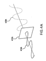
- pattern generator 206 is an LCD array, which comprises a plurality of LCD chips. Each LCD chip operates as is depicted in Figure 4A.
- the type of liquid crystal (LC) employed and how that LC material behaves in the presence of an electric field will determine its polarization and whether incident light is transmitted or not (in the case of a transmissive array), as is conventionally known in the LCD art.
- the LC material in an LCD chip may have properties such that if no voltage is applied to LCD chip 432A, the polarity of an incident polarized light beam wave 434A changes (i.e., "rotates") ninety degrees (90°).
- transmitted polarized light beam wave 436A is ninety degrees out of phase with respect to incident polarized light beam wave 434A. This occurs because of the refractive properties of the LC material of LCD chip 432A. Alternatively, application of a voltage to LCD chip 432A may not cause the polarity of polarized light beam wave 434A to rotate ninety degrees, thereby allowing light beam wave 434A to simply pass through with the same polarity. At voltages in-between, however, the polarization of the light is partly rotated and elliptically polarized. Alternatively, the LC material may have opposite properties such that if no voltage is applied, the polarity does not change, and if a voltage is applied, the polarity changes ninety degrees.
- the liquid crystal material of the LCD array has properties such that when no voltage is supplied to a pixel, the polarity of the resulting light beam 216 from that pixel is rotated by ninety degrees.
- a certain voltage a "no-polarity-change" voltage
- the polarity of the resulting light beam 216 from that pixel does not change.
- a polarizer 205B with the same polarity as the polarity of polarized illumination beam 204A is employed. In this configuration, light beams 216 incident on pixels of LCD array 206 with no voltage supplied thereto will be at the opposite polarity as polarizer 205B and will be blocked, producing no exposure in the corresponding areas of substrate 124.
- light beams 216 incident on pixels of LCD array 206 with the "no-polarity-change" voltage supplied will be at the same polarity as polarizer 205B and will be transmitted through as light beams 216A.
- Light beams 216A will then pass through reduction optics 118 as minimized light beams 220, and will expose substrate 124 at the highest intensity.
- the polarization of the light is partly rotated and elliptically polarized, allowing some light to pass through polarizer 205B, and therefore allowing greyscale levels to occur in light beams 216A.
- the liquid crystal material of the LCD array has properties such that when a certain voltage is supplied to a pixel (e.g., a "90-degree-polarity-change" voltage), the polarity of the resulting light beam 216 from that pixel is rotated by ninety degrees.
- a certain voltage e.g., a "90-degree-polarity-change" voltage
- the polarity of the resulting light beam 216 from that pixel does not change.
- the desired result is for the pixels with no voltage supplied thereto to produce no light at all, then the light resulting from pixels with no voltage supplied needs to be blocked.
- a polarizer with a polarity opposite of the polarity of polarized illumination beam 204A is employed. In this configuration, light beams 216 incident on pixels of LCD array 206 with no voltage supplied thereto will be at the opposite polarity as polarizer 205B and will be blocked, producing no exposure in the corresponding areas of substrate 124.
- light beams 216 incident on pixels of LCD array 206 with the "90-degree-polarity-change" voltage supplied will be at the same polarity as polarizer 205B and will be transmitted through as light beams 216A.
- Light beams 216A will then pass through reduction optics 118 as minimized light beams 220, and will expose substrate 124 at the highest intensity.
- the polarization of the light is partly rotated and elliptically polarized, allowing some light to pass through polarizer 205B, and therefore allowing greyscale levels to occur in light beams 216A.
- Reduction optics 118 comprises a plurality of lenses. Reduction optics 118 can encompass any suitable reduction optics for this purpose, as is to be appreciated by those skilled in the art.
- Minimized light beam 220 is then projected onto substrate 124 held by substrate stage 122. The intensity of the exposure on substrate 124 depends indirectly on the amount of voltage applied to each corresponding pixel of pattern generator 206, as previously described.
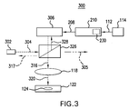
- FIG. 3 Another embodiment of the present invention is shown in FIG. 3.
- pattern generator 306 is a reflective LCD (RLCD) array.
- RLCD reflective LCD
- a significant difference between an LCD array and an RLCD array is that the incident light beam(s) for imaging the substrate is reflected off the RLCD, rather than being transmitted through.
- the polarization modulation occurs similarly in both LCD and RLCD arrays.
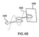
- an RLCD chip works as is depicted in Figure 4B.
- the LC material in an RLCD chip may have properties such that if no voltage is applied to RLCD chip 432B, the polarity of an incident polarized light beam wave 434B changes (i.e., "rotates") ninety degrees (90°).
- transmitted polarized light beam wave 436B is ninety degrees out of phase with respect to incident polarized light beam wave 434B.
- application of a voltage to RLCD chip 432B may not cause the polarity of polarized light beam wave 434A to rotate ninety degrees, thereby allowing light beam wave 434A to simply reflect from the RLCD with the same polarity.
- the polarization of the light is partly rotated and elliptically polarized.
- the LC material may have opposite properties such that if no voltage is applied, the polarity does not change, and if a voltage is applied, the polarity changes 90 degrees.
- a light source 302 outputs a light beam 304.
- Light beam 304 is directed toward polarizing beam splitter 326.
- Polarizing beam splitter 326 reflects a polarized beam 328 toward pattern generator 306.
- Polarizing beam splitter 326 can be any polarizing dichroic mirror as known in the art. It will be appreciated by those skilled in the art that a polarized beam 305 will pass through polarizing beam splitter 326 with the opposite polarity as polarized beam 328 and be lost from the system.
- the RLCD array of pattern generator 306 comprises a plurality of RLCD chips. Each pixel of each RLCD chip is provided with a voltage corresponding to instructions supplied by control signal 208. Pattern generator 306 reflects resulting light beams 316 back toward polarizing beam splitter 326. As with maskless optical writing system 200, the intensity of the resulting exposure on substrate 124 depends indirectly on the voltage supplied to each pixel and the resulting polarization modulation of the output light beams.
- the liquid crystal material of the RLCD array has properties such that when no voltage is supplied to a pixel, the polarity of resulting reflected light beam 316 from that pixel is rotated by ninety degrees. Reflected light beam 316 will then be at the correct polarity to pass directly through polarizing beam splitter 326.
- a voltage is supplied to a pixel (e.g., a "no-polarity-change" voltage)
- the polarity of resulting reflected light beam 316 from that pixel does not change and will again reflect from polarizing beam splitter 326 as beam 317 and be lost from the system.
- the polarization of resulting reflected beams 316 from those pixels is partly rotated and elliptically polarized, allowing some light to pass through polarizing beam splitter 326, and therefore allowing greyscale levels to occur in reflected light beams 316.
- the liquid crystal material of the RLCD array has properties such that when a certain voltage is supplied to a pixel (e.g., a "90-degree-polarity-change" voltage), the polarity of the resulting reflected light beam 316 from that pixel is rotated by ninety degrees. Reflected light beam 316 will then be at the correct polarity to pass directly through polarizing beam splitter 326.
- a certain voltage e.g., a "90-degree-polarity-change" voltage
- Reflected light beam 316 will then be at the correct polarity to pass directly through polarizing beam splitter 326.
- the polarity of resulting reflected light beam 316 from that pixel does not change and will again reflect from polarizing beam splitter 326 as beam 317 and be lost from the system.
- the polarization of resulting reflected beams 316 from those pixels is partly rotated and elliptically polarized, allowing some light to pass through polarizing beam splitter 326, and therefore allowing greyscale levels to occur in light beams 316.
- Reduction optics 118 comprises a plurality of lenses. Reduction optics 118 can encompass any suitable reduction optics for this purpose, as is to be appreciated by those skilled in the art.
- Minimized light beam 320 is then projected onto substrate 124 held by substrate stage 122. The intensity of the exposure on substrate 124 depends indirectly on the amount of voltage applied to each corresponding pixel of pattern generator 306, as previously described.
- pattern generators 206/306 are compatible with 157nm illumination to 248nm illumination, with 193nm illumination preferred.
- a "slit" area defines the area of projection onto a substrate.
- the size of a slit area is related to magnification, chip size, and the number of chips arrayed. According to embodiments of the present invention, multiple chips are laid out in an array.
- a slit area of approximately 8mm by 22mm is preferably used, which involves an array of chips.
- this area can be as small as 4mm by 12mm or as large as 16mm by 48mm, depending on the optics design. However, this area can be smaller or larger than this range, depending on the application in which the invention is used.
- the slit area for pattern generators used in a flat panel application could be as large as 8cm by 22cm or larger.
- Pattern generators used for projection televisions or cinema screens can cover even larger slit areas, used for screens of 50 feet or larger, for example. For large applications such as these, however, the pixel size will be large.
- maskless optical writing systems 200/300 can generate pixel sizes on a substrate from 20nm to 1.5mm, with a preferred size of approximately 50nm.
- reduction optics 118 can minimize a pattern image by a magnification range of .005X to 350X, with a magnification of 200X preferred.
- light source 202/302 is a pulsed excimer laser. Using this laser, individual voltage levels of individual pixels are changed between laser pulses. In embodiments of the present invention, the light source 202/302 provides polarized light.
- controller 210 comprises a pattern information manipulator 230.
- Pattern information manipulator 230 decodes pattern information received from data stream 112, and assigns the pattern information data on a pixel-by-pixel basis. According to an embodiment of the present invention, the pattern information manipulator 230 assigns greyscale values for each pixel.
- Embodiments of pattern information manipulator 230 can comprise hardware, software, or a combination of hardware and software.
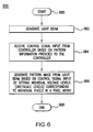
- FIG. 5 illustrates pattern information manipulator 230 in more detail.
- Data stream 112, containing pattern information enters pattern information manipulator 230 and is decoded at a decoder 540.
- Pixel addresses are generated at an address generator 542. Instructions for each pixel are stored in a memory 544 as a pixel "matrix" in a row-by-column manner.
- a pixel can correspond with an instruction to apply a "maximum" voltage, as depicted by pixel address 546.
- a pixel can correspond with an instruction to apply no voltage, as depicted by pixel address 548.
- a greyscale level of exposure can alternatively be assigned to a pixel by assigning a voltage that is in-between these two levels. For example, exposure at 75% is assigned to pixel address 550. It will be appreciated by those skilled in the art that some linearity correction is needed within the pattern information manipulator 230 of controller 210 to ensure that the greyscale effect is linear as compared to the voltages applied.
- a method 600 of generating a maskless pattern is illustrated in FIG. 6.
- the method starts at step 680 and immediately continues at step 682.
- a light beam is generated.
- a control signal input is received from a controller based on pattern information provided to the controller.
- a pattern image is generated from the light beam based on the control signal input.
- the pattern image is generated by setting individual voltage levels (i.e., greyscale levels) corresponding to individual pixels in a pixel array.
- Method 600 ends at step 688.
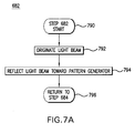
- step 682 of method 600 is carried out as depicted in FIG. 7A.
- Step 682 starts at step 790 and immediately continues to step 792.
- step 792 a light beam is generated.
- step 794 the light beam is reflected toward a pattern generator. The reflection can be accomplished by any beam splitter. In an embodiment, a polarized beam splitter is used.
- step 796 the method returns to step 684 of method 600.
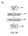
- step 682 of method 600 is carried out as depicted in FIG. 7B.
- Step 682 starts at step 790 and immediately continues to step 792.
- step 792 a light beam is generated.
- step 795 the light beam is polarized. Polarization of the light beam can be accomplished using any polarizer as is recognized by those skilled in the art.
- step 796 the method returns to step 684 of method 600.
- a method 800 of generating a maskless pattern is illustrated in FIG. 8.
- the method starts at step 802 and immediately continues at step 804.
- a polarized illumination is generated.
- a control signal input is received from a controller based on pattern information provided to the controller.
- a polarization state of the polarized illumination is modulated.
- a pattern image is generated from the modulated polarized illumination based on the control signal input.
- Method 800 ends at step 812.
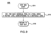
- step 808 of method 800 is carried out as depicted in FIG. 9.
- Step 808 starts at step 914 and immediately continues to step 916.
- step 916 a voltage level corresponding to a greyscale level (including black and white) is set for each individual pixel in a pixel array.
- step 918 the method returns to step 810 of method 800.
- a method 1000 of performing maskless lithography is illustrated in FIG. 10.
- the method starts at step 1020 and immediately continues at step 1022.
- a light beam is generated.
- a control signal input is received from a controller based on pattern information provided to the controller.
- a pattern image is generated from the light beam based on the control signal input.
- the pattern image is generated by setting individual voltage levels (i.e., greyscale levels) corresponding to individual pixels in a pixel array.
- the pattern image is minimized by reduction optics for projection onto a substrate.
- the substrate is positioned relative to the reduction optics.
- the pattern image is received on the substrate.
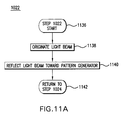
- step 1022 of method 1000 is carried out as depicted in FIG. 11A.
- Step 1022 starts at step 1136 and immediately continues to step 1138.
- step 1138 a light beam is generated.
- step 1140 the light beam is reflected toward a pattern generator. The reflection can be accomplished by any beam splitter, as is recognized by those skilled in the art. In an embodiment, a polarized beam splitter is used.
- step 1142 the method returns to step 1024 of method 1000.
- step 1022 of method 1000 is carried out as depicted in FIG. 11B.
- Step 1022 starts at step 1136 and immediately continues to step 1138.
- step 1138 a light beam is generated.
- step 1141 the light beam is polarized. Polarization of the light beam can be accomplished using any polarizer, as is recognized by those skilled in the art.
- step 1142 the method returns to step 1024 of method 1000.
- a method 1200 of performing maskless lithography, according to an embodiment of the present invention, is illustrated in FIG. 12.
- the method starts at step 1250 and immediately continues at step 1252.
- a polarized illumination is generated.
- a control signal input is received from a controller based on pattern information provided to the controller.
- a polarization state of the polarized illumination is modulated.
- a pattern image is generated from the modulated polarized illumination based on the control signal input.
- the pattern image is minimized by reduction optics for projection onto a substrate.
- the substrate is positioned relative to the reduction optics.
- the pattern image is received on the substrate.
- Method 1200 ends at step 1270.
- step 1252 of method 1200 is carried out as depicted in FIG. 13.
- Step 1252 starts at step 1372 and immediately continues to step 1374.
- step 1374 a polarized illumination is generated.
- step 1376 the polarized illumination is reflected toward a pattern generator. The reflection can be accomplished by any beam splitter. In an embodiment, a polarized beam splitter is used.
- step 1378 the method returns to step 1254 of method 1200.
- step 1256 of method 1200 is carried out as depicted in FIG. 14.
- Step 1256 starts at step 1480 and immediately continues to step 1482.
- step 1482 a voltage level corresponding to a greyscale level (including black and white) is set for each individual pixel in a pixel array.
- step 1484 the method returns to step 1258 of method 1200.
- a method 1500 of performing maskless lithography, according to an embodiment of the present invention, is illustrated in FIG. 15.
- the method starts at step 1502 and immediately continues at step 1504.
- a light beam is generated.
- the light beam is polarized.
- a control signal input is received from a controller based on pattern information provided to the controller.
- a polarization state of the polarized light beam is modulated.
- a pattern image is generated from the modulated polarized light beam based on the control signal input.
- the pattern image is generated by setting individual voltage levels (i.e., greyscale levels) corresponding to individual pixels in a pixel array.
- the pattern image is polarized.
- the pattern image is minimized by reduction optics for projection onto a substrate.
- the substrate is positioned relative to the reduction optics.
- the pattern image is received on the substrate.
- a method 1600 of performing maskless lithography, according to an embodiment of the present invention, is illustrated in FIG. 16.
- the method starts at step 1602 and immediately continues at step 1604.
- a light beam is generated.
- the light beam is polarized.
- the polarized light beam is reflected toward a pattern generator.
- a control signal input is received from a controller based on pattern information provided to the controller.
- a polarization state of the polarized light beam is modulated.
- a pattern image is generated from the modulated polarized light beam based on the control signal input.
- the pattern image is generated by setting individual voltage levels (i.e., greyscale levels) corresponding to individual pixels in a pixel array.
- the pattern image is reflected toward reduction optics.
- the pattern image is polarized.
- the pattern image is minimized by reduction optics for projection onto a substrate.
- the substrate is positioned relative to the reduction optics.
- the pattern image is received on the substrate.
- One advantage of the present invention is that it can be used as a phase shift mask. By applying a voltage over more than one cycle of light, a phase shift occurs that imparts useful characteristics similar to a phase shift mask as understood by those skilled in the art.
- To use the present invention as a phase shift mask one changes the voltage past the point where the polarization has rotated 90 degrees. This pixel-by-pixel phase interference has the same effect as a phase shift mask, improving the resolution of the system.
- Another advantage of the present invention is that a pattern image can be easily moved by shifting the voltage levels applied to each pixel depending on exactly where the pattern needs to be placed.
- the placement of the pattern image is shifted when the individual voltage levels set for corresponding pixels are shifted in one direction by the same number of pixel rows or columns.
- a further advantage of the present invention is that greyscaling in the manner described allows the pattern to be easily moved relative to the definition grid.
- the light from each pixel merges into the light from other pixels.
- the light from the edge row of pixels "spills" over and gradually changes from light to dark in a graduated effect. How quickly the transition from light to dark occurs can be controlled by partly turning on the pixels in the transition region. In this way, the light levels of the pixels are manipulated by applying the appropriate voltage levels to "move" an edge of the pattern.
- This feature of the invention may be used to allow a transition (the gradual change from light to dark) to occur at a boundary that does not correspond to a basic grid boundary.
- the result may be a transition that is not occurring at a location where one of the basic grid boundaries occurs.
- the light levels of the pixels on either side of that boundary can be manipulated by applying the appropriate voltage levels to those pixels.
- Chart 1760 shows the plotting of light intensity variation across an exposure edge.
- the pixel At a certain voltage applied to a pixel, the pixel is considered completely “off,” as shown by plot 1765.
- the pixel At a different voltage applied to the pixel, the pixel is considered completely “on,” as shown by plot 1770.
- the distance between the pattern edges when completely “off” (plot 1765) versus completely “on” (plot 1770) is 40 nm, which in this example is the width of the pixel. Varying the voltage level applied to the pixel to a voltage between the two voltage levels for "on” and “off” allow the pattern edge to be located at intermediate positions, as shown by the data plots in-between plot 1765 and 1770.
- FIGS. 18 and 19 also illustrate the shifting of an exposed edge through the use of greyscaling as described in accordance with embodiments of the present invention.
- pixel rows 1882 of pixel grid 1880 are shown as completely “off.”
- Pixel rows 1884 are shown as completely “on.”
- Plot 1888 shows a sharp transition between light and dark.
- FIG. 19 shows the movement of the exposed pattern edge.
- Pixel rows 1982 of pixel grid 1980 are shown as completely "off.”
- Pixel rows 1984 are shown as completely "on.”
- Pixel row 1986 is shown at an intermediate state of "on,” in this case at 25% "on.” Setting pixel row 1986 to an intermediate state of on, in effect, has moved the edge of the pattern slightly to the left.
- Plot 1988 shows the transition between light and dark as a more graduated transition than that of FIG. 18.
- This disclosure presents a maskless pattern writing system that acts as a light valve to control pattern imagery, on a pixel by pixel basis, for the purpose of direct writing patterns.
Landscapes
- Engineering & Computer Science (AREA)
- General Engineering & Computer Science (AREA)
- Physics & Mathematics (AREA)
- General Physics & Mathematics (AREA)
- Health & Medical Sciences (AREA)
- Life Sciences & Earth Sciences (AREA)
- Medical Informatics (AREA)
- Mechanical Engineering (AREA)
- Pathology (AREA)
- Surgery (AREA)
- Nuclear Medicine, Radiotherapy & Molecular Imaging (AREA)
- Optics & Photonics (AREA)
- Biophysics (AREA)
- Radiology & Medical Imaging (AREA)
- Biomedical Technology (AREA)
- Heart & Thoracic Surgery (AREA)
- Molecular Biology (AREA)
- High Energy & Nuclear Physics (AREA)
- Animal Behavior & Ethology (AREA)
- General Health & Medical Sciences (AREA)
- Public Health (AREA)
- Veterinary Medicine (AREA)
- Exposure And Positioning Against Photoresist Photosensitive Materials (AREA)
- Exposure Of Semiconductors, Excluding Electron Or Ion Beam Exposure (AREA)
- Liquid Crystal (AREA)
Applications Claiming Priority (2)
| Application Number | Priority Date | Filing Date | Title |
|---|---|---|---|
| US755470 | 2004-01-13 | ||
| US10/755,470 US7012674B2 (en) | 2004-01-13 | 2004-01-13 | Maskless optical writer |
Publications (2)
| Publication Number | Publication Date |
|---|---|
| EP1555574A2 true EP1555574A2 (de) | 2005-07-20 |
| EP1555574A3 EP1555574A3 (de) | 2008-01-09 |
Family
ID=34620661
Family Applications (1)
| Application Number | Title | Priority Date | Filing Date |
|---|---|---|---|
| EP05000082A Withdrawn EP1555574A3 (de) | 2004-01-13 | 2005-01-04 | Maskenloses System zur Erzeugung eines Musters |
Country Status (7)
| Country | Link |
|---|---|
| US (2) | US7012674B2 (de) |
| EP (1) | EP1555574A3 (de) |
| JP (1) | JP4459822B2 (de) |
| KR (1) | KR100702072B1 (de) |
| CN (1) | CN1661473A (de) |
| SG (1) | SG113549A1 (de) |
| TW (1) | TWI296737B (de) |
Families Citing this family (11)
| Publication number | Priority date | Publication date | Assignee | Title |
|---|---|---|---|---|
| US7012674B2 (en) * | 2004-01-13 | 2006-03-14 | Asml Holding N.V. | Maskless optical writer |
| KR20070104444A (ko) * | 2005-01-28 | 2007-10-25 | 에이에스엠엘 홀딩 엔.브이. | 전체적 최적화에 기초한 무마스크 리소그래피래스터라이제이션 기술을 위한 방법 및 시스템 |
| US7936445B2 (en) * | 2006-06-19 | 2011-05-03 | Asml Netherlands B.V. | Altering pattern data based on measured optical element characteristics |
| US9140978B2 (en) | 2010-10-12 | 2015-09-22 | Weng-Dah Ken | Semiconductor multi-project or multi-product wafer process |
| US8949749B2 (en) * | 2012-10-23 | 2015-02-03 | Taiwan Semiconductor Manufacturing Co., Ltd. | Layout design for electron-beam high volume manufacturing |
| KR102120624B1 (ko) | 2013-04-04 | 2020-06-10 | 삼성디스플레이 주식회사 | Glv를 이용한 디지털 노광기 및 dmd를 이용한 디지털 노광기 |
| WO2015036002A1 (en) * | 2013-09-14 | 2015-03-19 | Carl Zeiss Smt Gmbh | Method of operating a microlithographic projection apparatus |
| CN104298077B (zh) * | 2014-09-26 | 2016-07-06 | 中国科学院长春光学精密机械与物理研究所 | 滚动灰度光刻的dmd动作方法 |
| US11681228B2 (en) * | 2018-06-19 | 2023-06-20 | Ev Group E. Thallner Gmbh | Method and apparatus for illuminating image points |
| WO2023004493A1 (en) * | 2021-07-26 | 2023-02-02 | Technologies Digitho Inc. | Photolithography mask and photolithography system comprising said photolithography mask |
| JP2024532663A (ja) | 2021-07-26 | 2024-09-10 | テクノロジーズ デジソー インコーポレイテッド | フォトリソグラフィマスク及び係るフォトリソグラフィマスクを備えたフォトリソグラフィシステム |
Family Cites Families (41)
| Publication number | Priority date | Publication date | Assignee | Title |
|---|---|---|---|---|
| US5523193A (en) * | 1988-05-31 | 1996-06-04 | Texas Instruments Incorporated | Method and apparatus for patterning and imaging member |
| JP2938568B2 (ja) * | 1990-05-02 | 1999-08-23 | フラウンホファー・ゲゼルシャフト・ツール・フォルデルング・デル・アンゲバンテン・フォルシュング・アインゲトラーゲネル・フェライン | 照明装置 |
| US5229872A (en) * | 1992-01-21 | 1993-07-20 | Hughes Aircraft Company | Exposure device including an electrically aligned electronic mask for micropatterning |
| US6219015B1 (en) * | 1992-04-28 | 2001-04-17 | The Board Of Directors Of The Leland Stanford, Junior University | Method and apparatus for using an array of grating light valves to produce multicolor optical images |
| JP3224041B2 (ja) * | 1992-07-29 | 2001-10-29 | 株式会社ニコン | 露光方法及び装置 |
| JP2616660B2 (ja) * | 1993-06-21 | 1997-06-04 | 日本電気株式会社 | 厚膜配線パターンの露光装置および厚膜の成形方法 |
| US5729331A (en) * | 1993-06-30 | 1998-03-17 | Nikon Corporation | Exposure apparatus, optical projection apparatus and a method for adjusting the optical projection apparatus |
| JP3339149B2 (ja) * | 1993-12-08 | 2002-10-28 | 株式会社ニコン | 走査型露光装置ならびに露光方法 |
| JP3541327B2 (ja) | 1994-09-26 | 2004-07-07 | 富士通株式会社 | 露光装置 |
| US5677703A (en) * | 1995-01-06 | 1997-10-14 | Texas Instruments Incorporated | Data loading circuit for digital micro-mirror device |
| US5530482A (en) * | 1995-03-21 | 1996-06-25 | Texas Instruments Incorporated | Pixel data processing for spatial light modulator having staggered pixels |
| US5699168A (en) * | 1995-06-22 | 1997-12-16 | Texas Instruments Incorporated | Grayscale printing with sliding window memory |
| EP0991959B1 (de) * | 1996-02-28 | 2004-06-23 | Kenneth C. Johnson | Mikrolinsen-rastereinrichtung für mikrolithografie und für konfokale mikroskopie mit grossem aufnahmefeld |
| JP4126096B2 (ja) | 1997-01-29 | 2008-07-30 | マイクロニック レーザー システムズ アクチボラゲット | 感光性被覆を有する基板上に集束レーザ放射により構造物を製作する方法と装置 |
| US6177980B1 (en) * | 1997-02-20 | 2001-01-23 | Kenneth C. Johnson | High-throughput, maskless lithography system |
| SE509062C2 (sv) | 1997-02-28 | 1998-11-30 | Micronic Laser Systems Ab | Dataomvandlingsmetod för en laserskrivare med flera strålar för mycket komplexa mikrokolitografiska mönster |
| US5982553A (en) * | 1997-03-20 | 1999-11-09 | Silicon Light Machines | Display device incorporating one-dimensional grating light-valve array |
| US6291110B1 (en) * | 1997-06-27 | 2001-09-18 | Pixelligent Technologies Llc | Methods for transferring a two-dimensional programmable exposure pattern for photolithography |
| KR100280832B1 (ko) * | 1997-12-02 | 2001-04-02 | 정선종 | 노광 장비용 프로그래머블 마스크 |
| US5998069A (en) * | 1998-02-27 | 1999-12-07 | Micron Technology, Inc. | Electrically programmable photolithography mask |
| SE9800665D0 (sv) * | 1998-03-02 | 1998-03-02 | Micronic Laser Systems Ab | Improved method for projection printing using a micromirror SLM |
| US6356340B1 (en) * | 1998-11-20 | 2002-03-12 | Advanced Micro Devices, Inc. | Piezo programmable reticle for EUV lithography |
| JP2001185476A (ja) * | 1999-12-27 | 2001-07-06 | Mitsubishi Electric Corp | 投影露光装置 |
| KR100827874B1 (ko) * | 2000-05-22 | 2008-05-07 | 가부시키가이샤 니콘 | 노광 장치, 노광 장치의 제조 방법, 노광 방법, 마이크로 장치의 제조 방법, 및 디바이스의 제조 방법 |
| US6407766B1 (en) * | 2000-07-18 | 2002-06-18 | Eastman Kodak Company | Method and apparatus for printing to a photosensitive media using multiple spatial light modulators |
| US6580490B1 (en) * | 2000-10-30 | 2003-06-17 | Eastman Kodak Company | Method and apparatus for printing images in multiple formats using a spatial light modulator |
| US7095484B1 (en) | 2001-06-27 | 2006-08-22 | University Of South Florida | Method and apparatus for maskless photolithography |
| US6544698B1 (en) | 2001-06-27 | 2003-04-08 | University Of South Florida | Maskless 2-D and 3-D pattern generation photolithography |
| TW554411B (en) | 2001-08-23 | 2003-09-21 | Nikon Corp | Exposure apparatus |
| JP2005533365A (ja) | 2001-11-07 | 2005-11-04 | アプライド マテリアルズ インコーポレイテッド | マスクレスの光子−電子スポット格子アレイ印刷装置 |
| JP3563384B2 (ja) * | 2001-11-08 | 2004-09-08 | 大日本スクリーン製造株式会社 | 画像記録装置 |
| US7023528B2 (en) * | 2002-06-10 | 2006-04-04 | International Business Machines Corporation | Hybrid electronic mask |
| JP2005222963A (ja) * | 2002-06-12 | 2005-08-18 | Asml Netherlands Bv | リソグラフィ装置およびその装置の製造方法 |
| AU2003243779A1 (en) * | 2002-06-25 | 2004-01-06 | University Of South Florida | Method and apparatus for maskless photolithography |
| SG115590A1 (en) * | 2002-11-27 | 2005-10-28 | Asml Netherlands Bv | Lithographic projection apparatus and device manufacturing method |
| US6812477B2 (en) * | 2002-12-04 | 2004-11-02 | Texas Instruments Incorporated | Integrated circuit identification |
| US6870554B2 (en) * | 2003-01-07 | 2005-03-22 | Anvik Corporation | Maskless lithography with multiplexed spatial light modulators |
| EP1480080A1 (de) * | 2003-05-22 | 2004-11-24 | ASML Netherlands B.V. | Lithographischer Apparat und Verfahren zur Herstellung einer Vorrichtung |
| EP1482373A1 (de) * | 2003-05-30 | 2004-12-01 | ASML Netherlands B.V. | Lithographischer Apparat und Verfahren zur Herstellung eines Artikels |
| US6831768B1 (en) | 2003-07-31 | 2004-12-14 | Asml Holding N.V. | Using time and/or power modulation to achieve dose gray-scaling in optical maskless lithography |
| US7012674B2 (en) * | 2004-01-13 | 2006-03-14 | Asml Holding N.V. | Maskless optical writer |
-
2004
- 2004-01-13 US US10/755,470 patent/US7012674B2/en not_active Expired - Lifetime
-
2005
- 2005-01-04 EP EP05000082A patent/EP1555574A3/de not_active Withdrawn
- 2005-01-05 TW TW094100282A patent/TWI296737B/zh not_active IP Right Cessation
- 2005-01-05 SG SG200500026A patent/SG113549A1/en unknown
- 2005-01-12 KR KR1020050002792A patent/KR100702072B1/ko not_active Expired - Fee Related
- 2005-01-13 JP JP2005006630A patent/JP4459822B2/ja not_active Expired - Fee Related
- 2005-01-13 CN CN2005100043455A patent/CN1661473A/zh active Pending
-
2006
- 2006-01-24 US US11/337,691 patent/US7548301B2/en not_active Expired - Fee Related
Also Published As
| Publication number | Publication date |
|---|---|
| KR20050074320A (ko) | 2005-07-18 |
| SG113549A1 (en) | 2005-08-29 |
| US20050151953A1 (en) | 2005-07-14 |
| TW200523673A (en) | 2005-07-16 |
| US20060119827A1 (en) | 2006-06-08 |
| EP1555574A3 (de) | 2008-01-09 |
| CN1661473A (zh) | 2005-08-31 |
| TWI296737B (en) | 2008-05-11 |
| KR100702072B1 (ko) | 2007-04-03 |
| US7012674B2 (en) | 2006-03-14 |
| JP2005210115A (ja) | 2005-08-04 |
| JP4459822B2 (ja) | 2010-04-28 |
| US7548301B2 (en) | 2009-06-16 |
Similar Documents
| Publication | Publication Date | Title |
|---|---|---|
| US7738077B2 (en) | Patterning device utilizing sets of stepped mirrors and method of using same | |
| KR100794280B1 (ko) | 리소그래피 장치 및 디바이스 제조방법 | |
| US7110082B2 (en) | Optical system for maskless lithography | |
| EP1882987A2 (de) | System und Verfahren zum Ausgleich kritischer Dimensionsungleichförmigkeit in einem Lithographiesystem | |
| KR20090017982A (ko) | 리소그래피 장치 및 디바이스 제조방법 | |
| JP2010272878A (ja) | リソグラフィ投影装置およびデバイス製造方法 | |
| JP2009145904A (ja) | 二重位相ステップエレメントを使用するパターニングデバイスおよびその使用方法 | |
| JP2001135562A (ja) | リソグラフィ装置 | |
| JP2006013518A (ja) | リソグラフィ装置およびデバイス製造方法 | |
| JP4023541B2 (ja) | リソグラフ用投影装置およびデバイス製造方法 | |
| US7012674B2 (en) | Maskless optical writer | |
| KR100589230B1 (ko) | 리소그래피장치 및 디바이스제조방법 | |
| US20060017902A1 (en) | Lithographic apparatus having double telecentric illumination | |
| US7242456B2 (en) | System and method utilizing a lithography tool having modular illumination, pattern generator, and projection optics portions | |
| US7286137B2 (en) | Method and system for constrained pixel graytones interpolation for pattern rasterization | |
| JP4373976B2 (ja) | バイナリ、減衰フェーズシフトおよび交番フェーズシフトマスクをエミュレートするマスクレスリソグラフィ用のシステムおよび装置および方法 | |
| JP2014504455A (ja) | リソグラフィ装置においてパターニングデバイスを制御する方法、デバイス製造方法、及びリソグラフィ装置 |
Legal Events
| Date | Code | Title | Description |
|---|---|---|---|
| PUAI | Public reference made under article 153(3) epc to a published international application that has entered the european phase |
Free format text: ORIGINAL CODE: 0009012 |
|
| AK | Designated contracting states |
Kind code of ref document: A2 Designated state(s): AT BE BG CH CY CZ DE DK EE ES FI FR GB GR HU IE IS IT LI LT LU MC NL PL PT RO SE SI SK TR |
|
| AX | Request for extension of the european patent |
Extension state: AL BA HR LV MK YU |
|
| PUAL | Search report despatched |
Free format text: ORIGINAL CODE: 0009013 |
|
| AK | Designated contracting states |
Kind code of ref document: A3 Designated state(s): AT BE BG CH CY CZ DE DK EE ES FI FR GB GR HU IE IS IT LI LT LU MC NL PL PT RO SE SI SK TR |
|
| AX | Request for extension of the european patent |
Extension state: AL BA HR LV MK YU |
|
| 17P | Request for examination filed |
Effective date: 20080708 |
|
| AKX | Designation fees paid |
Designated state(s): DE FR GB IT NL |
|
| 17Q | First examination report despatched |
Effective date: 20090120 |
|
| STAA | Information on the status of an ep patent application or granted ep patent |
Free format text: STATUS: THE APPLICATION IS DEEMED TO BE WITHDRAWN |
|
| 18D | Application deemed to be withdrawn |
Effective date: 20090731 |