EP1552603B1 - Leistungsverstärkersystem - Google Patents
Leistungsverstärkersystem Download PDFInfo
- Publication number
- EP1552603B1 EP1552603B1 EP03792459A EP03792459A EP1552603B1 EP 1552603 B1 EP1552603 B1 EP 1552603B1 EP 03792459 A EP03792459 A EP 03792459A EP 03792459 A EP03792459 A EP 03792459A EP 1552603 B1 EP1552603 B1 EP 1552603B1
- Authority
- EP
- European Patent Office
- Prior art keywords
- power
- power amplifier
- power supply
- supply voltage
- sub
- Prior art date
- Legal status (The legal status is an assumption and is not a legal conclusion. Google has not performed a legal analysis and makes no representation as to the accuracy of the status listed.)
- Expired - Lifetime
Links
- 230000001934 delay Effects 0.000 claims abstract description 5
- 238000000034 method Methods 0.000 claims description 10
- 238000007493 shaping process Methods 0.000 claims description 7
- 238000004891 communication Methods 0.000 claims description 3
- 238000010295 mobile communication Methods 0.000 description 4
- 230000003595 spectral effect Effects 0.000 description 2
- 230000003321 amplification Effects 0.000 description 1
- 230000000694 effects Effects 0.000 description 1
- 230000008030 elimination Effects 0.000 description 1
- 238000003379 elimination reaction Methods 0.000 description 1
- 238000001914 filtration Methods 0.000 description 1
- 238000003199 nucleic acid amplification method Methods 0.000 description 1
- 230000007704 transition Effects 0.000 description 1
Images
Classifications
-
- H—ELECTRICITY
- H03—ELECTRONIC CIRCUITRY
- H03G—CONTROL OF AMPLIFICATION
- H03G3/00—Gain control in amplifiers or frequency changers
- H03G3/20—Automatic control
- H03G3/30—Automatic control in amplifiers having semiconductor devices
- H03G3/3036—Automatic control in amplifiers having semiconductor devices in high-frequency amplifiers or in frequency-changers
- H03G3/3042—Automatic control in amplifiers having semiconductor devices in high-frequency amplifiers or in frequency-changers in modulators, frequency-changers, transmitters or power amplifiers
-
- H—ELECTRICITY
- H03—ELECTRONIC CIRCUITRY
- H03F—AMPLIFIERS
- H03F1/00—Details of amplifiers with only discharge tubes, only semiconductor devices or only unspecified devices as amplifying elements
- H03F1/02—Modifications of amplifiers to raise the efficiency, e.g. gliding Class A stages, use of an auxiliary oscillation
- H03F1/0205—Modifications of amplifiers to raise the efficiency, e.g. gliding Class A stages, use of an auxiliary oscillation in transistor amplifiers
- H03F1/0211—Modifications of amplifiers to raise the efficiency, e.g. gliding Class A stages, use of an auxiliary oscillation in transistor amplifiers with control of the supply voltage or current
- H03F1/0216—Continuous control
- H03F1/0222—Continuous control by using a signal derived from the input signal
-
- H—ELECTRICITY
- H03—ELECTRONIC CIRCUITRY
- H03F—AMPLIFIERS
- H03F1/00—Details of amplifiers with only discharge tubes, only semiconductor devices or only unspecified devices as amplifying elements
- H03F1/02—Modifications of amplifiers to raise the efficiency, e.g. gliding Class A stages, use of an auxiliary oscillation
- H03F1/0205—Modifications of amplifiers to raise the efficiency, e.g. gliding Class A stages, use of an auxiliary oscillation in transistor amplifiers
- H03F1/0211—Modifications of amplifiers to raise the efficiency, e.g. gliding Class A stages, use of an auxiliary oscillation in transistor amplifiers with control of the supply voltage or current
- H03F1/0244—Stepped control
-
- H—ELECTRICITY
- H03—ELECTRONIC CIRCUITRY
- H03G—CONTROL OF AMPLIFICATION
- H03G3/00—Gain control in amplifiers or frequency changers
- H03G3/004—Control by varying the supply voltage
-
- H—ELECTRICITY
- H03—ELECTRONIC CIRCUITRY
- H03G—CONTROL OF AMPLIFICATION
- H03G3/00—Gain control in amplifiers or frequency changers
- H03G3/20—Automatic control
- H03G3/30—Automatic control in amplifiers having semiconductor devices
- H03G3/3036—Automatic control in amplifiers having semiconductor devices in high-frequency amplifiers or in frequency-changers
- H03G3/3042—Automatic control in amplifiers having semiconductor devices in high-frequency amplifiers or in frequency-changers in modulators, frequency-changers, transmitters or power amplifiers
- H03G3/3047—Automatic control in amplifiers having semiconductor devices in high-frequency amplifiers or in frequency-changers in modulators, frequency-changers, transmitters or power amplifiers for intermittent signals, e.g. burst signals
Definitions
- This invention relates to a linear power amplifier system, in particular for use with 3 rd generation mobile communication systems.
- Power amplifiers can be generally categorised into three modes of operation, class A, B and C.
- class A or class B amplifier amplifies a sinusoidal signal, so maximum efficiency is achieved if the output is a sinewave extending over the full range of voltage and minimum efficiency is achieved if the sinewave amplitude is minimum.
- Class B amplifiers are biased at zero, so the output produces current pulses with half the cycle missing which is reconstituted by subsequent filtering.
- Class C amplifiers are negatively biased and non-linear, in this case a low signal level also leads to low efficiency.
- EER envelope elimination and restoration
- US2002/0084844 describes a system in which first and second amplifier stages are provided, such that if a signal power level is below a predetermined threshold, the signal is directed to a first stage amplifier to amplify the input signal and if the level is above the threshold the signal is directed to the second stage amplifier.
- This system is somewhat limited in its application since it views the input signal as being simply low power or high power. Furthermore, it is inefficient in hardware terms because of the requirement to construct two amplifier stages, although only one will ever be used at any time.
- JP57 002107 describes an audio power amplifier designed to reduce switching distortion by adapting the power supply voltage to the input signal level.
- an RF power amplifier system comprises a control circuit; a delay circuit and a power amplifier; wherein the control circuit comprises a detector for detecting an instantaneous power level of an input signal from a signal source; a threshold comparator; and a power supply voltage source; and a pulse shaping filter; wherein the threshold comparator is provided with a plurality of preset thresholds; wherein the threshold comparator compares the power level detected at the detector with the preset thresholds; wherein the power supply voltage is switched according to the output of the threshold comparator, and wherein the delay device delays the input signal to the power amplifier to enable the power supply voltage to be adapted to the power level detected at the detector, such that the efficiency of the power amplifier is optimised.
- the present invention provides an efficient linear power amplifier in which the power supply voltage to the amplifier is changed according to the threshold reached by the detected input signal power level. Multiple thresholds are preset and associated with a suitable power supply voltage. This is a flexible system which provides a significant improvement in efficiency over conventional systems.
- the system may be operated with two preset thresholds, but preferably, at least three preset thresholds are provided.
- the power supply voltage source comprises a plurality of preset power supply voltages associated with respective power level thresholds.
- At least four preset power supply voltages are provided.
- the power amplifier is a Class B amplifier and a filter is provided at the output of the amplifier to reconstitute the amplified input signal.
- a code division multiple access (CDMA) communication system comprises a power amplifier system according to the first aspect.
- CDMA code division multiple access
- CDMA systems use radio waves which have varying amplitudes, but the present invention is able to cope with this whilst maintaining efficiency of the amplifier by switching the power supply voltage according to the input signal power level.
- a method of operating a power amplifier system comprises applying an input signal from a signal source, to a control circuit and a delay device; detecting at a detector in the control circuit an instantaneous power level of an input signal; comparing the detected power level with a plurality of preset thresholds in a threshold comparator, switching a power supply voltage according to the output of the threshold comparator, and passing the power supply voltage through the pulse shaping filter; wherein the delay device delays the input signal to the power amplifier to enable the power supply voltage to be adapted to the detected power level, such that the efficiency of the power amplifier is optimised.
- a plurality of power supply voltage levels, associated with respective power level thresholds, are preset.
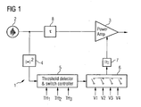
- FIG. 1 shows one example of a power amplifier system 1 according to the present invention.
- An amplitude variant source signal 2 containing information that is to be transmitted, is input to the system.
- the signal follows a first path to a power amplifier 3 via a control circuit.
- the control circuit comprises an envelope detector 4, which provides a value that is proportional to the instantaneous power of the input signal 2.
- This value is applied to a threshold detector 5 which has N, in this case 3, preset thresholds, although more can be set if appropriate.
- An output of the threshold detector 5 controls switching of a switch unit 6 between N+1, in this case 4, discrete power supply voltages for the power amplifier.
- the chosen voltage then passes through a pulse shaping filter 7 to the power amplifier 3.
- the signal follows a second path to the power amplifier via a time delay 8, so that the power supply voltage of the power amplifier is set to the correct value before the signal to which it relates is amplified in the power amplifier 3.
- the threshold detector 5 compares pre-set threshold values TH 1 , TH 2 , and TH 3 with the value representing the instantaneous power provided by the envelope detector 4. The output of this comparison provides a control signal to turn the appropriate switch on in the switch unit 6.
- a voltage V 1 is applied to the power amplifier 3.
- a voltage V 2 is applied to the power amplifier; if the envelope is between thresholds TH 2 and TH 3 , then a voltage V 3 is applied to the power amplifier and finally, for all envelope values above the pre-set threshold TH 3 , a voltage, V 4 is selected by the switch unit 6.
- the invention is not restricted to three discrete threshold values, and in fact any number may be used.
- the number of pre-set threshold values and the corresponding supply voltages are determined to match the properties of the transmitted signal and the characteristics of the power amplifier.
- a further feature of the present invention is the provision of the pulse-shaping filter 7.
- This filter limits the slew rate of the power supply voltage as the DC voltage is switched between the discrete values. This in turn minimizes the undesirable spectral spreading of the transmitted signal that may be caused by the power amplifier as the supply voltage is varied.
- the purpose of the time delay 8 in the second path is to match the overall delay in the first path containing the envelope detector 4, the threshold detector 5, the switch unit 6 and the pulse-shaping filter 7 with the delay of the power amplifier. This ensures that the signal and the appropriate power supply voltage are applied synchronously at the correct instant.
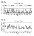
- Fig. 2a illustrates an example of how the instantaneous power determined in the envelope detector 4 varies for a particular input signal.
- the graph shows normalised power against time and three thresholds TH 1 , TH 2 and TH 3 for the normalised power are set, at values of 0.9, 0.5 and 0.2 respectively. From Fig. 2b it is possible to see how the power supply voltage changes with each threshold transition.
- a normalised DC voltage is shown against time. It takes a finite period of time to reach the new value, hence the need to delay the signal into the power amplifier, so that the power supply voltage is correct.
- the time delay 8, envelope detector 4 and threshold detector 5 may be implemented digitally in the baseband section of a transmitter or alternatively these elements may be realized by analog circuitry.
- the efficiency improvement described herein is applicable in conjunction with both feed forward and pre-distortion linearisation techniques.
Landscapes
- Engineering & Computer Science (AREA)
- Power Engineering (AREA)
- Amplifiers (AREA)
Claims (8)
- HF-Leistungsverstärkersystem, wobei das System Folgendes umfasst: eine Steuerschaltung (1); eine Verzögerungsschaltung (8) und einen HF-Leistungsverstärker (3); wobei die Steuerschaltung Folgendes umfasst: einen Detektor (4) zum Detektieren eines Momentanleistungspegels eines Eingangssignals aus einer Signalquelle (2); einen Schwellenkomparator (5); eine Stromversorgungsspannungsquelle (6); und ein Impulsformungsfilter (7); wobei der Schwellenkomparator mit mehreren voreingestellten Schwellen (TH1, TH2, TH3) ausgestattet ist; wobei der Schwellenkomparator (5) den in dem Detektor (4) detektierten Leistungspegel mit den voreingestellten Schwellen vergleicht; wobei die Stromversorgungsspannung gemäß der Ausgabe des Schwellenkomparators (5) umgeschaltet wird; und wobei die Verzögerungseinrichtung (8) das Eingangssignal des Leistungsverstärkers (3) verzögert, um eine Anpassung der Stromversorgungsspannung an den in dem Detektor (4) detektierten Leistungspegel zu ermöglichen, so dass der Wirkungsgrad des Leistungsverstärkers optimiert wird.
- Leistungsverstärkersystem nach Anspruch 1, wobei mindestens drei voreingestellte Schwellen (TH1, TH2, TH3) vorgesehen sind.
- Leistungsverstärkersystem nach Anspruch 1 oder Anspruch 2, wobei die Stromversorgungsspannungsquelle (6) mehrere voreingestellte Stromversorgungsspannungen (V1, V2, V3, V4) umfasst, die mit jeweiligen Leistungspegelschwellen (TH1, TH2, TH3) assoziiert sind.
- Leistungsverstärkersystem nach Anspruch 3, wobei mindestens vier voreingestellte Stromversorgungsspannungen (V1, V2, V3, V4) vorgesehen sind.
- Leistungsverstärkersystem nach einem der vorhergehenden Ansprüche, wobei der Leistungsverstärker (3) ein Verstärker der Klasse B ist und wobei am Ausgang des Verstärkers ein Filter vorgesehen ist, um das verstärkte Eingangssignal zu rekonstituieren.
- CDMA-Kommunikationssystem, das ein Leistungsverstärkersystem nach einem der vorherigen Ansprüche umfasst.
- Verfahren zum Betrieb eines Leistungsverstärkersystem mit den folgenden Schritten: Anlegen eines Eingangssignals aus einer Signalquelle (2) an eine Steuerschaltung (1) und eine Verzögerungseinrichtung (8); Detektieren eines Momentanleistungspegels eines Eingangssignals in einem Detektor (4) in der Steuerschaltung (1); Vergleichen des detektierten Leistungspegels mit mehreren voreingestellten Schwellen (TH1, TH2, TH3) in einem Schwellenkomparator (5); Umschalten einer Stromversorgungsspannung (V1, V2, V3, V4) gemäß der Ausgabe des Schwellenkomparators; und Leiten der Stromversorgungsspannung durch ein Impulsformungsfilter (7); wobei die Verzögerungseinrichtung (8) das Eingangssignal des Leistungsverstärkers (3) verzögert, um eine Anpassung der Stromversorgungsspannung an den detektierten Leistungspegel zu ermöglichen, so dass der Wirkungsgrad des Leistungsverstärkers optimiert wird.
- Verfahren nach Anspruch 7, wobei mehrere Stromversorgungsspannungspegel (V1, V2, V3, V4) voreingestellt werden, die mit jeweiligen Leistungspegelschwellen (TH1, TH2, TH3) assoziiert sind.
Applications Claiming Priority (3)
| Application Number | Priority Date | Filing Date | Title |
|---|---|---|---|
| GB0219466 | 2002-08-21 | ||
| GBGB0219466.0A GB0219466D0 (en) | 2002-08-21 | 2002-08-21 | Multi-carrier power amplifier with switched PSU voltages |
| PCT/GB2003/003414 WO2004019486A1 (en) | 2002-08-21 | 2003-08-06 | A power amplifier system |
Publications (2)
| Publication Number | Publication Date |
|---|---|
| EP1552603A1 EP1552603A1 (de) | 2005-07-13 |
| EP1552603B1 true EP1552603B1 (de) | 2009-07-01 |
Family
ID=9942713
Family Applications (1)
| Application Number | Title | Priority Date | Filing Date |
|---|---|---|---|
| EP03792459A Expired - Lifetime EP1552603B1 (de) | 2002-08-21 | 2003-08-06 | Leistungsverstärkersystem |
Country Status (8)
| Country | Link |
|---|---|
| US (1) | US20050242880A1 (de) |
| EP (1) | EP1552603B1 (de) |
| CN (1) | CN100431262C (de) |
| AT (1) | ATE435518T1 (de) |
| AU (1) | AU2003260715A1 (de) |
| DE (1) | DE60328215D1 (de) |
| GB (1) | GB0219466D0 (de) |
| WO (1) | WO2004019486A1 (de) |
Families Citing this family (30)
| Publication number | Priority date | Publication date | Assignee | Title |
|---|---|---|---|---|
| GB2398648B (en) * | 2003-02-19 | 2005-11-09 | Nujira Ltd | Power supply stage for an amplifier |
| DE602005000437T2 (de) | 2004-07-08 | 2007-10-31 | Sony United Kingdom Ltd., Weybridge | Leistungsregelung für Leistungsverstärker |
| JP4487754B2 (ja) | 2004-12-10 | 2010-06-23 | 日本電気株式会社 | 携帯電話端末およびその電圧供給制御装置、ならびに電圧供給制御方法 |
| JP4874106B2 (ja) | 2005-01-06 | 2012-02-15 | パナソニック株式会社 | 極座標変調装置及びそれを用いた無線通信機器 |
| CN101401261B (zh) | 2006-02-03 | 2012-11-21 | 匡坦斯公司 | 功率放大器控制器电路 |
| US8095090B2 (en) * | 2006-02-03 | 2012-01-10 | Quantance, Inc. | RF power amplifier controller circuit |
| US7869542B2 (en) | 2006-02-03 | 2011-01-11 | Quantance, Inc. | Phase error de-glitching circuit and method of operating |
| US7761065B2 (en) * | 2006-02-03 | 2010-07-20 | Quantance, Inc. | RF power amplifier controller circuit with compensation for output impedance mismatch |
| US8032097B2 (en) | 2006-02-03 | 2011-10-04 | Quantance, Inc. | Amplitude error de-glitching circuit and method of operating |
| US7917106B2 (en) * | 2006-02-03 | 2011-03-29 | Quantance, Inc. | RF power amplifier controller circuit including calibrated phase control loop |
| US7933570B2 (en) * | 2006-02-03 | 2011-04-26 | Quantance, Inc. | Power amplifier controller circuit |
| US7962174B2 (en) * | 2006-07-12 | 2011-06-14 | Andrew Llc | Transceiver architecture and method for wireless base-stations |
| TW200904015A (en) * | 2007-03-15 | 2009-01-16 | Powercast Corp | Multiple frequency transmitter, receiver, and systems thereof |
| WO2008134420A2 (en) * | 2007-04-25 | 2008-11-06 | Marvell World Trade Ltd. | Power amplifier adjustment for transmit beamforming in multi-antenna wireless systems |
| US7466195B2 (en) * | 2007-05-18 | 2008-12-16 | Quantance, Inc. | Error driven RF power amplifier control with increased efficiency |
| US7783269B2 (en) * | 2007-09-20 | 2010-08-24 | Quantance, Inc. | Power amplifier controller with polar transmitter |
| US8014735B2 (en) * | 2007-11-06 | 2011-09-06 | Quantance, Inc. | RF power amplifier controlled by estimated distortion level of output signal of power amplifier |
| US8018277B2 (en) * | 2008-09-09 | 2011-09-13 | Quantance, Inc. | RF power amplifier system with impedance modulation |
| US7782134B2 (en) * | 2008-09-09 | 2010-08-24 | Quantance, Inc. | RF power amplifier system with impedance modulation |
| US7777566B1 (en) * | 2009-02-05 | 2010-08-17 | Quantance, Inc. | Amplifier compression adjustment circuit |
| US8446219B2 (en) * | 2009-06-17 | 2013-05-21 | Futurewei Technologies, Inc. | Class-G line driver control signal |
| EP2670047A1 (de) | 2012-06-01 | 2013-12-04 | Sequans Communications | HF-Kommunikationen |
| CN104469620B (zh) * | 2014-11-24 | 2018-05-08 | 青岛歌尔声学科技有限公司 | 一种音频输出功率大范围可调的声学产品 |
| CN107066013B (zh) * | 2017-06-21 | 2018-06-15 | 电子科技大学 | 一种测井仪功放电源自适应调整装置 |
| CN107066000B (zh) * | 2017-06-21 | 2018-06-15 | 电子科技大学 | 一种测井仪功放电源自适应调整方法 |
| JP6904179B2 (ja) * | 2017-09-06 | 2021-07-14 | ヤマハ株式会社 | 増幅器、音響機器および制御方法 |
| DE102019131226A1 (de) * | 2018-11-19 | 2020-05-20 | Maxim Integrated Products, Inc. | Treiberschaltkreis und assoziierte Verfahren |
| CN109698674A (zh) * | 2018-12-11 | 2019-04-30 | 四川九洲电器集团有限责任公司 | 一种功率回退装置和电子设备及其控制方法 |
| CN109511040B (zh) * | 2018-12-27 | 2020-09-22 | 歌尔科技有限公司 | 一种耳语放大方法、装置及耳机 |
| US11917378B2 (en) * | 2021-06-17 | 2024-02-27 | Maxim Integrated Products, Inc. | Systems and methods for controlling powerstage supply modulation via audio interface |
Family Cites Families (11)
| Publication number | Priority date | Publication date | Assignee | Title |
|---|---|---|---|---|
| JPS572107A (en) * | 1980-06-04 | 1982-01-07 | Pioneer Electronic Corp | Power supply circuit of electric power amplifier |
| DE69409968T2 (de) * | 1993-11-30 | 1998-10-29 | Crown International, Inc., Elkhart, Ind. | Schaltnetzteil für einen leistungsverstärker |
| US5787336A (en) * | 1994-11-08 | 1998-07-28 | Space Systems/Loral, Inc. | Satellite communication power management system |
| US6028486A (en) * | 1997-10-07 | 2000-02-22 | Telefonaktiebolaget Lm Ericsson | Method and apparatus for reducing power dissipation in multi-carrier amplifiers |
| US6157253A (en) * | 1999-09-03 | 2000-12-05 | Motorola, Inc. | High efficiency power amplifier circuit with wide dynamic backoff range |
| SE517622C2 (sv) * | 1999-12-17 | 2002-06-25 | Ericsson Telefon Ab L M | Anordning för att minska en linjedrivares effektförlust |
| KR20020083735A (ko) * | 2001-04-30 | 2002-11-04 | 고범종 | 고효율 전력증폭기 |
| US6714071B1 (en) * | 2001-06-25 | 2004-03-30 | Nortel Networks Limited | Gate modulation for high power amplifiers |
| US7031457B2 (en) * | 2001-11-30 | 2006-04-18 | Texas Instruments Incorporated | Programmable peak detector for use with zero-overhead Class G line drivers |
| US6788151B2 (en) * | 2002-02-06 | 2004-09-07 | Lucent Technologies Inc. | Variable output power supply |
| US7339426B2 (en) * | 2004-03-19 | 2008-03-04 | Powerwave Technologies, Inc. | High efficiency linear amplifier employing dynamically controlled back off |
-
2002
- 2002-08-21 GB GBGB0219466.0A patent/GB0219466D0/en not_active Ceased
-
2003
- 2003-08-06 EP EP03792459A patent/EP1552603B1/de not_active Expired - Lifetime
- 2003-08-06 US US10/525,306 patent/US20050242880A1/en not_active Abandoned
- 2003-08-06 WO PCT/GB2003/003414 patent/WO2004019486A1/en not_active Ceased
- 2003-08-06 CN CNB03819855XA patent/CN100431262C/zh not_active Expired - Fee Related
- 2003-08-06 AT AT03792459T patent/ATE435518T1/de not_active IP Right Cessation
- 2003-08-06 AU AU2003260715A patent/AU2003260715A1/en not_active Abandoned
- 2003-08-06 DE DE60328215T patent/DE60328215D1/de not_active Expired - Lifetime
Also Published As
| Publication number | Publication date |
|---|---|
| WO2004019486A1 (en) | 2004-03-04 |
| ATE435518T1 (de) | 2009-07-15 |
| AU2003260715A1 (en) | 2004-03-11 |
| DE60328215D1 (de) | 2009-08-13 |
| CN1675827A (zh) | 2005-09-28 |
| AU2003260715A8 (en) | 2004-03-11 |
| CN100431262C (zh) | 2008-11-05 |
| GB0219466D0 (en) | 2002-10-02 |
| EP1552603A1 (de) | 2005-07-13 |
| US20050242880A1 (en) | 2005-11-03 |
Similar Documents
| Publication | Publication Date | Title |
|---|---|---|
| EP1552603B1 (de) | Leistungsverstärkersystem | |
| US9979353B2 (en) | High efficiency variable voltage supply | |
| US7518441B2 (en) | Signal processor for use with a power amplifier in a wireless circuit | |
| US8254496B2 (en) | Power amplifier and radio wave transmitter having the same | |
| CA2505189C (en) | Systems and methods of dynamic bias switching for radio frequency power amplifiers | |
| US6982593B2 (en) | Switching amplifier architecture | |
| KR101105926B1 (ko) | 무선 통신 디바이스에서 신호 구성 기반 송신기 조정 | |
| US7855599B2 (en) | Power amplifier | |
| CA2459545C (en) | Method and apparatus for providing a supply voltage based on an envelope of a radio frequency signal | |
| EP1150422B1 (de) | Adaptive Kompensation der Phasenverzerrung eines Trägersignals | |
| KR101481725B1 (ko) | 무선 통신시스템의 전력 송신 장치 및 방법 | |
| CN100550604C (zh) | 产生调制波信号的传输电路以及包括该电路的通信设备 | |
| US6300830B1 (en) | Multiplexed input envelope restoration scheme for linear high-efficiency power amplification | |
| JP5389567B2 (ja) | 高周波増幅器および高効率化方法 | |
| US20050068793A1 (en) | Pulse width modulated power supply | |
| Jouzdani et al. | High efficiency delta-sigma transmitter architecture with gate bias modulation for wireless applications |
Legal Events
| Date | Code | Title | Description |
|---|---|---|---|
| PUAI | Public reference made under article 153(3) epc to a published international application that has entered the european phase |
Free format text: ORIGINAL CODE: 0009012 |
|
| 17P | Request for examination filed |
Effective date: 20050211 |
|
| AK | Designated contracting states |
Kind code of ref document: A1 Designated state(s): AT BE BG CH CY CZ DE DK EE ES FI FR GB GR HU IE IT LI LU MC NL PT RO SE SI SK TR |
|
| RAP1 | Party data changed (applicant data changed or rights of an application transferred) |
Owner name: NOKIA SIEMENS NETWORKS GMBH & CO. KG |
|
| RAP3 | Party data changed (applicant data changed or rights of an application transferred) |
Owner name: NOKIA SIEMENS NETWORKS S.P.A. |
|
| RAP3 | Party data changed (applicant data changed or rights of an application transferred) |
Owner name: NOKIA SIEMENS NETWORKS GMBH & CO. KG |
|
| GRAP | Despatch of communication of intention to grant a patent |
Free format text: ORIGINAL CODE: EPIDOSNIGR1 |
|
| GRAS | Grant fee paid |
Free format text: ORIGINAL CODE: EPIDOSNIGR3 |
|
| GRAA | (expected) grant |
Free format text: ORIGINAL CODE: 0009210 |
|
| AK | Designated contracting states |
Kind code of ref document: B1 Designated state(s): AT BE BG CH CY CZ DE DK EE ES FI FR GB GR HU IE IT LI LU MC NL PT RO SE SI SK TR |
|
| REG | Reference to a national code |
Ref country code: GB Ref legal event code: FG4D |
|
| REG | Reference to a national code |
Ref country code: CH Ref legal event code: EP |
|
| REG | Reference to a national code |
Ref country code: IE Ref legal event code: FG4D |
|
| REF | Corresponds to: |
Ref document number: 60328215 Country of ref document: DE Date of ref document: 20090813 Kind code of ref document: P |
|
| PGFP | Annual fee paid to national office [announced via postgrant information from national office to epo] |
Ref country code: ES Payment date: 20090820 Year of fee payment: 7 |
|
| PG25 | Lapsed in a contracting state [announced via postgrant information from national office to epo] |
Ref country code: SI Free format text: LAPSE BECAUSE OF FAILURE TO SUBMIT A TRANSLATION OF THE DESCRIPTION OR TO PAY THE FEE WITHIN THE PRESCRIBED TIME-LIMIT Effective date: 20090701 |
|
| PGFP | Annual fee paid to national office [announced via postgrant information from national office to epo] |
Ref country code: AT Payment date: 20090814 Year of fee payment: 7 |
|
| NLV1 | Nl: lapsed or annulled due to failure to fulfill the requirements of art. 29p and 29m of the patents act | ||
| PG25 | Lapsed in a contracting state [announced via postgrant information from national office to epo] |
Ref country code: EE Free format text: LAPSE BECAUSE OF FAILURE TO SUBMIT A TRANSLATION OF THE DESCRIPTION OR TO PAY THE FEE WITHIN THE PRESCRIBED TIME-LIMIT Effective date: 20090701 Ref country code: SE Free format text: LAPSE BECAUSE OF FAILURE TO SUBMIT A TRANSLATION OF THE DESCRIPTION OR TO PAY THE FEE WITHIN THE PRESCRIBED TIME-LIMIT Effective date: 20090701 Ref country code: FI Free format text: LAPSE BECAUSE OF FAILURE TO SUBMIT A TRANSLATION OF THE DESCRIPTION OR TO PAY THE FEE WITHIN THE PRESCRIBED TIME-LIMIT Effective date: 20090701 Ref country code: AT Free format text: LAPSE BECAUSE OF FAILURE TO SUBMIT A TRANSLATION OF THE DESCRIPTION OR TO PAY THE FEE WITHIN THE PRESCRIBED TIME-LIMIT Effective date: 20090701 Ref country code: ES Free format text: LAPSE BECAUSE OF FAILURE TO SUBMIT A TRANSLATION OF THE DESCRIPTION OR TO PAY THE FEE WITHIN THE PRESCRIBED TIME-LIMIT Effective date: 20091012 |
|
| PG25 | Lapsed in a contracting state [announced via postgrant information from national office to epo] |
Ref country code: NL Free format text: LAPSE BECAUSE OF FAILURE TO SUBMIT A TRANSLATION OF THE DESCRIPTION OR TO PAY THE FEE WITHIN THE PRESCRIBED TIME-LIMIT Effective date: 20090701 |
|
| PG25 | Lapsed in a contracting state [announced via postgrant information from national office to epo] |
Ref country code: PT Free format text: LAPSE BECAUSE OF FAILURE TO SUBMIT A TRANSLATION OF THE DESCRIPTION OR TO PAY THE FEE WITHIN THE PRESCRIBED TIME-LIMIT Effective date: 20091102 Ref country code: BG Free format text: LAPSE BECAUSE OF FAILURE TO SUBMIT A TRANSLATION OF THE DESCRIPTION OR TO PAY THE FEE WITHIN THE PRESCRIBED TIME-LIMIT Effective date: 20091001 Ref country code: MC Free format text: LAPSE BECAUSE OF NON-PAYMENT OF DUE FEES Effective date: 20090831 |
|
| REG | Reference to a national code |
Ref country code: CH Ref legal event code: PL |
|
| PG25 | Lapsed in a contracting state [announced via postgrant information from national office to epo] |
Ref country code: CH Free format text: LAPSE BECAUSE OF NON-PAYMENT OF DUE FEES Effective date: 20090831 Ref country code: RO Free format text: LAPSE BECAUSE OF FAILURE TO SUBMIT A TRANSLATION OF THE DESCRIPTION OR TO PAY THE FEE WITHIN THE PRESCRIBED TIME-LIMIT Effective date: 20090701 Ref country code: DK Free format text: LAPSE BECAUSE OF FAILURE TO SUBMIT A TRANSLATION OF THE DESCRIPTION OR TO PAY THE FEE WITHIN THE PRESCRIBED TIME-LIMIT Effective date: 20090701 Ref country code: LI Free format text: LAPSE BECAUSE OF NON-PAYMENT OF DUE FEES Effective date: 20090831 Ref country code: CZ Free format text: LAPSE BECAUSE OF FAILURE TO SUBMIT A TRANSLATION OF THE DESCRIPTION OR TO PAY THE FEE WITHIN THE PRESCRIBED TIME-LIMIT Effective date: 20090701 |
|
| PLBE | No opposition filed within time limit |
Free format text: ORIGINAL CODE: 0009261 |
|
| STAA | Information on the status of an ep patent application or granted ep patent |
Free format text: STATUS: NO OPPOSITION FILED WITHIN TIME LIMIT |
|
| PG25 | Lapsed in a contracting state [announced via postgrant information from national office to epo] |
Ref country code: BE Free format text: LAPSE BECAUSE OF FAILURE TO SUBMIT A TRANSLATION OF THE DESCRIPTION OR TO PAY THE FEE WITHIN THE PRESCRIBED TIME-LIMIT Effective date: 20090701 Ref country code: SK Free format text: LAPSE BECAUSE OF FAILURE TO SUBMIT A TRANSLATION OF THE DESCRIPTION OR TO PAY THE FEE WITHIN THE PRESCRIBED TIME-LIMIT Effective date: 20090701 |
|
| 26N | No opposition filed |
Effective date: 20100406 |
|
| PG25 | Lapsed in a contracting state [announced via postgrant information from national office to epo] |
Ref country code: IE Free format text: LAPSE BECAUSE OF NON-PAYMENT OF DUE FEES Effective date: 20090806 |
|
| PG25 | Lapsed in a contracting state [announced via postgrant information from national office to epo] |
Ref country code: GR Free format text: LAPSE BECAUSE OF FAILURE TO SUBMIT A TRANSLATION OF THE DESCRIPTION OR TO PAY THE FEE WITHIN THE PRESCRIBED TIME-LIMIT Effective date: 20091002 |
|
| PG25 | Lapsed in a contracting state [announced via postgrant information from national office to epo] |
Ref country code: IT Free format text: LAPSE BECAUSE OF FAILURE TO SUBMIT A TRANSLATION OF THE DESCRIPTION OR TO PAY THE FEE WITHIN THE PRESCRIBED TIME-LIMIT Effective date: 20090701 |
|
| PG25 | Lapsed in a contracting state [announced via postgrant information from national office to epo] |
Ref country code: LU Free format text: LAPSE BECAUSE OF NON-PAYMENT OF DUE FEES Effective date: 20090806 |
|
| PG25 | Lapsed in a contracting state [announced via postgrant information from national office to epo] |
Ref country code: HU Free format text: LAPSE BECAUSE OF FAILURE TO SUBMIT A TRANSLATION OF THE DESCRIPTION OR TO PAY THE FEE WITHIN THE PRESCRIBED TIME-LIMIT Effective date: 20100102 |
|
| PG25 | Lapsed in a contracting state [announced via postgrant information from national office to epo] |
Ref country code: TR Free format text: LAPSE BECAUSE OF FAILURE TO SUBMIT A TRANSLATION OF THE DESCRIPTION OR TO PAY THE FEE WITHIN THE PRESCRIBED TIME-LIMIT Effective date: 20090701 |
|
| PG25 | Lapsed in a contracting state [announced via postgrant information from national office to epo] |
Ref country code: CY Free format text: LAPSE BECAUSE OF FAILURE TO SUBMIT A TRANSLATION OF THE DESCRIPTION OR TO PAY THE FEE WITHIN THE PRESCRIBED TIME-LIMIT Effective date: 20090701 |
|
| REG | Reference to a national code |
Ref country code: DE Ref legal event code: R081 Ref document number: 60328215 Country of ref document: DE Owner name: NOKIA SOLUTIONS AND NETWORKS GMBH & CO. KG, DE Free format text: FORMER OWNER: NOKIA SIEMENS NETWORKS GMBH & CO. KG, 81541 MUENCHEN, DE Effective date: 20140731 |
|
| REG | Reference to a national code |
Ref country code: FR Ref legal event code: CD Owner name: NOKIA SOLUTIONS AND NETWORKS GMBH & CO.KG, DE Effective date: 20150211 |
|
| REG | Reference to a national code |
Ref country code: FR Ref legal event code: PLFP Year of fee payment: 13 |
|
| REG | Reference to a national code |
Ref country code: FR Ref legal event code: PLFP Year of fee payment: 14 |
|
| REG | Reference to a national code |
Ref country code: FR Ref legal event code: PLFP Year of fee payment: 15 |
|
| REG | Reference to a national code |
Ref country code: FR Ref legal event code: PLFP Year of fee payment: 16 |
|
| PGFP | Annual fee paid to national office [announced via postgrant information from national office to epo] |
Ref country code: FR Payment date: 20210714 Year of fee payment: 19 |
|
| PGFP | Annual fee paid to national office [announced via postgrant information from national office to epo] |
Ref country code: DE Payment date: 20210630 Year of fee payment: 19 Ref country code: GB Payment date: 20210701 Year of fee payment: 19 |
|
| REG | Reference to a national code |
Ref country code: DE Ref legal event code: R119 Ref document number: 60328215 Country of ref document: DE |
|
| GBPC | Gb: european patent ceased through non-payment of renewal fee |
Effective date: 20220806 |
|
| PG25 | Lapsed in a contracting state [announced via postgrant information from national office to epo] |
Ref country code: FR Free format text: LAPSE BECAUSE OF NON-PAYMENT OF DUE FEES Effective date: 20220831 Ref country code: DE Free format text: LAPSE BECAUSE OF NON-PAYMENT OF DUE FEES Effective date: 20230301 |
|
| PG25 | Lapsed in a contracting state [announced via postgrant information from national office to epo] |
Ref country code: GB Free format text: LAPSE BECAUSE OF NON-PAYMENT OF DUE FEES Effective date: 20220806 |