EP1548853A1 - Josephson-tunnelübergang mit hochtemperatur-supraleiter - Google Patents
Josephson-tunnelübergang mit hochtemperatur-supraleiter Download PDFInfo
- Publication number
- EP1548853A1 EP1548853A1 EP03753937A EP03753937A EP1548853A1 EP 1548853 A1 EP1548853 A1 EP 1548853A1 EP 03753937 A EP03753937 A EP 03753937A EP 03753937 A EP03753937 A EP 03753937A EP 1548853 A1 EP1548853 A1 EP 1548853A1
- Authority
- EP
- European Patent Office
- Prior art keywords
- high temperature
- tunnel junction
- josephson tunnel
- temperature superconductive
- superconductive josephson
- Prior art date
- Legal status (The legal status is an assumption and is not a legal conclusion. Google has not performed a legal analysis and makes no representation as to the accuracy of the status listed.)
- Granted
Links
Images


Classifications
-
- H—ELECTRICITY
- H10—SEMICONDUCTOR DEVICES; ELECTRIC SOLID-STATE DEVICES NOT OTHERWISE PROVIDED FOR
- H10N—ELECTRIC SOLID-STATE DEVICES NOT OTHERWISE PROVIDED FOR
- H10N60/00—Superconducting devices
- H10N60/10—Junction-based devices
- H10N60/12—Josephson-effect devices
- H10N60/124—Josephson-effect devices comprising high-Tc ceramic materials
-
- H—ELECTRICITY
- H10—SEMICONDUCTOR DEVICES; ELECTRIC SOLID-STATE DEVICES NOT OTHERWISE PROVIDED FOR
- H10N—ELECTRIC SOLID-STATE DEVICES NOT OTHERWISE PROVIDED FOR
- H10N60/00—Superconducting devices
- H10N60/01—Manufacture or treatment
- H10N60/0912—Manufacture or treatment of Josephson-effect devices
- H10N60/0941—Manufacture or treatment of Josephson-effect devices comprising high-Tc ceramic materials
Definitions
- the present invention relates to a high temperature superconductive Josephson tunnel junction. More particularly, the invention relates to a high temperature superconductive Josephson tunnel junction of which a plasma frequency varies depending on an intersecting angle.
- a Josephson tunnel junction device using a superconductor is a basic superconductive device and it has been applied as a high frequency device, an SFQ device (a switching device utilizing flux of line of magnetic force), a SQUID magnetic sensor device and others. Further enhancement of performance is expected if the Josephson tunnel junction device can be made of a high temperature superconductor.
- the inventors of the present application have already proposed formation of a Josephson junction in or near a bond of whisker crystals by intersecting whisker crystals of a high temperature superconductor and by heat treatment as a means of solving a technical problem of easily and quickly forming a Josephson junction having an excellent properties without requiring any expensive fine processing equipment (Japanese Patent Application No. 2000-250269).
- This application has not laid open at present, but it specifically proposes that a Josephson junction is formed by disposing two whisker crystals of a bismuth 2212 high temperature superconductor in a cross on an MgO substrate and putting the MgO substrate in a furnace for heat treatment in a baking condition of temperature of 850 °C, oxygen partial pressure of 70% and baking time of 30 minutes.
- the present invention is further advanced from the technology of the previous proposal and it is intended to provide a high temperature superconductive Josephson tunnel junction of which a plasma frequency varies depending on an intersecting angle, as a leading technology for creating a high temperature superconductive Josephson tunnel junction device capable of controlling properties.
- the present invention provides a high temperature superconductive Josephson junction, wherein two single crystals of a high temperature superconductor are bonded on a substrate in a range of intersecting angles of 0 degree to 90 degrees, a single high temperature superconductive Josephson tunnel junction is formed in a bonded portion, and a plasma frequency of the high temperature superconductive Josephson tunnel junction varies depending on an intersecting angle (claim 1).
- the two single crystals are any one of a whisker, a finely processed single crystal and a thin film, or a combination of two types of them (claim 2)
- the high temperature superconductor is a bismuth compound and its superconductive phase is any one of 2212 phase, 2201 phase and 2223 phase, or a combination of two or more types of them (claim 3).
- a high temperature superconductive Josephson tunnel junction of the invention is specifically described below with examples.
- a high temperature superconductive Josephson tunnel junction of the present invention is, as described above, a single high temperature superconductive Josephson tunnel junction formed in a bonded portion where two single crystals of a high temperature superconductor is bonded on a substrate in a range of intersecting angles of 0 degree to 90 degrees.
- a thin insulator layer is sandwiched between superconductors and the insulator layer is formed at an interface of two crystals. Therefore, in the high temperature superconductive Josephson tunnel junction of the invention, use of two single crystals, in one aspect, is for formation of an appropriate insulator layer at an interface. That is, a single Josephson tunnel junction is formed because the insulator layer formed at the interface of two single crystals is used. Unlike a polycrystal, a single crystal is uniform in an azimuth of a crystal. Therefore, as described below, in other aspect, the use of two single crystals is for controlling a plasma frequency fp of a high temperature Josephson tunnel junction by varying a critical electric current density based on an intersecting angle of the two single crystals.
- an intersecting angle of two high temperature superconductor single crystals bonded on the substrate that is, an angle not larger of two angles formed by two intersecting bismuth high temperature superconductor single crystals, is in a range of 0 degree to 90 degrees.
- a plasma frequency fp of the high temperature superconductive Josephson tunnel junction which intersects and is bonded in the range varies because a critical current density Jc changes depending on an intersecting angle.
- a plasma frequency fp varies depending on an intersecting angle and therefore the plasma frequency fp can be controlled by varying an intersecting angle of two high temperature superconductor single crystals to be bonded on the substrate.
- the plasma frequency peculiar to a high temperature superconductor generally ranges from hundreds of GHz to several THz and hence a high temperature superconductive Josephson tunnel device using a high temperature superconductor can respond to higher frequencies, but could not respond to lower frequencies.
- a plasma frequency fp can be changed in a range of two or three digits or more from a general plasma frequency peculiar to a high temperature superconductor to several GHz.
- high frequency response is observed, for example, at 20 GHz, which has been impossible to respond to. Theoretically, it is expected to respond to lower frequencies.
- IcRn a product of a critical current density and a shunt resistance, a value representing a signal processing capacity of a Josephson junction
- IcRn a product of a critical current density and a shunt resistance, a value representing a signal processing capacity of a Josephson junction
- a respondable maximum operating frequency fmax is also in proportion to the IcRn, as the IcRn increases, the fmax is considered to be higher.
- a high temperature superconductive Josephson tunnel junction device utilizing the high temperature superconductive Josephson tunnel junction of the invention is applied, for example, to a high frequency receiver, a receiver enhanced in a frequency property from fp to fmax will be possible.
- two single crystals of a high temperature superconductor are disposed on a substrate at an intersecting angle in a range of 0 degree to 90 degrees and the two single crystals are bonded by heat treatment as is similar to the previous proposal.
- a condition of heat treatment is temperature ranging from 0 degree to a melting point of a high temperature superconductor and an oxygen partial pressure ranging from 0 to 100%.
- Bonding faces of the two high temperature superconductor single crystals are any one of face a, face b and face c, or a combination of two faces of them.
- the two thin high temperature superconductor single crystals are any one of a whisker, a finely processed single crystal and a thin film, or a combination of two types of them.
- a high temperature superconductor used in the high temperature superconductive Josephson tunnel junction of the invention is not particularly specified in a material classification and may be properly selected from various materials generally regarded as a high temperature superconductor.
- a bismuth high temperature superconductor is selected and a superconductive phase in this case is any one of 2212 phase, 2201 phase and 2223 phase, or a combination of two or more types of them.
- a high temperature superconductor may be properly adjusted in composition, by adding elements or replacing elements, as far as a superconductive property may not be spoiled.
- Two whisker single crystals of 2212 phase of bismuth high temperature superconductor were disposed on an MgO substrate by intersecting in a range of 0 degree to 90 degrees, were put in an electric furnace to heat in a condition of temperature of 850 degrees and oxygen partial pressure of 70%, and were bonded together mutually on face c.
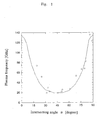
- the plasma frequency fp of the high temperature superconductive Josephson tunnel junction varied depending on change of an intersecting angle of two whisker single crystals.
- the plasma frequency fp of the high temperature superconductive Josephson tunnel junction showed high values peculiar to a high temperature superconductor at 0 degree and 90 degrees, but dropped to a bottom of about 20 GHz around 45 degrees.
- a greater change of plasma frequency fp than that in the graph in Fig. 1 may be expected.
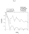
- a critical current density is determined by dividing a current value before standardization by area and it is a value proportional to the axis of ordinates in the graph in Fig. 3. It is hence known from the graph in Fig. 3 that critical current densities change periodically by application of a magnetic field. This phenomenon is known as a Fraunhofer pattern and it shows that the high temperature superconductive Josephson tunnel junction responds to a magnetic field. This Fraunhofer pattern is a basic property of a SQUID magnetic sensor.
- Two whisker single crystals of 2212 phase of bismuth high temperature superconductor were disposed on an MgO substrate by intersecting at an intersecting angle of 90 degrees and put in an electric furnace to heat in a condition of temperature of 850 degrees and oxygen partial pressure of 70%. Face b and face c were bonded.
- Fig. 4 is a graph showing a current-voltage property of a high temperature superconductive Josephson tunnel junction bonded between face b and face c.
- a single high temperature superconductive Josephson tunnel junction was obtained. That is, there is a region where no voltage generates at low currents and it means that a superconductive current is flowing in the junction.
- a current flows over a critical current value, a voltage is generated suddenly. This voltage generation corresponds to a jump appearing in the graph in Fig. 4. Since only one jump is recorded, it is confirmed that a single high temperature superconductive Josephson tunnel junction is obtained.
- every phenomenon that is confirmed in example 1 similarly occurs in the high temperature superconductive Josephson tunnel junction bonded between face b and face c.
- the present invention is not limited to the examples alone, but may be variously modified in a type of a high temperature superconductor, a shape of a single crystal, a condition of heat treatment and other details.
Landscapes
- Engineering & Computer Science (AREA)
- Chemical & Material Sciences (AREA)
- Ceramic Engineering (AREA)
- Manufacturing & Machinery (AREA)
- Superconductor Devices And Manufacturing Methods Thereof (AREA)
Applications Claiming Priority (3)
| Application Number | Priority Date | Filing Date | Title |
|---|---|---|---|
| JP2002275873 | 2002-09-20 | ||
| JP2002275873A JP4552007B2 (ja) | 2002-09-20 | 2002-09-20 | 高温超伝導ジョセフソントンネル接合構造における交差角度の設定方法 |
| PCT/JP2003/011912 WO2004027885A1 (ja) | 2002-09-20 | 2003-09-18 | 高温超伝導ジョセフソントンネル接合 |
Publications (3)
| Publication Number | Publication Date |
|---|---|
| EP1548853A1 true EP1548853A1 (de) | 2005-06-29 |
| EP1548853A4 EP1548853A4 (de) | 2007-03-28 |
| EP1548853B1 EP1548853B1 (de) | 2010-12-22 |
Family
ID=32025045
Family Applications (1)
| Application Number | Title | Priority Date | Filing Date |
|---|---|---|---|
| EP03753937A Expired - Lifetime EP1548853B1 (de) | 2002-09-20 | 2003-09-18 | Verfahrung zum variieren der plasmafrequenz eines josephson-tunnelübergangs mit hochtemperatur-supraleiter |
Country Status (7)
| Country | Link |
|---|---|
| US (1) | US20050215436A1 (de) |
| EP (1) | EP1548853B1 (de) |
| JP (1) | JP4552007B2 (de) |
| AT (1) | ATE492909T1 (de) |
| DE (1) | DE60335476D1 (de) |
| DK (1) | DK1548853T3 (de) |
| WO (1) | WO2004027885A1 (de) |
Families Citing this family (2)
| Publication number | Priority date | Publication date | Assignee | Title |
|---|---|---|---|---|
| US7610071B2 (en) * | 2006-03-27 | 2009-10-27 | Uchicago Argonne, Llc | Tunable, superconducting, surface-emitting teraherz source |
| EP4352664A4 (de) | 2021-06-11 | 2025-04-30 | Seeqc Inc. | System und verfahren zur flussvorspannung für supraleitende quantenschaltungen |
Family Cites Families (3)
| Publication number | Priority date | Publication date | Assignee | Title |
|---|---|---|---|---|
| US5306705A (en) * | 1991-07-18 | 1994-04-26 | Board Of Trustees Of The Leland Stanford Junior University | Superconductor-normal-superconductor with distributed Sharvin point contacts |
| JP3690823B2 (ja) * | 1994-03-29 | 2005-08-31 | 独立行政法人科学技術振興機構 | 超伝導接合体 |
| DE60134923D1 (de) * | 2000-08-21 | 2008-09-04 | Nat Inst For Materials Science | Verfahren zur Herstellung eines hochtemperatursupraleitenden Josephson-Übergangs |
-
2002
- 2002-09-20 JP JP2002275873A patent/JP4552007B2/ja not_active Expired - Lifetime
-
2003
- 2003-09-18 DK DK03753937.6T patent/DK1548853T3/da active
- 2003-09-18 US US10/528,076 patent/US20050215436A1/en not_active Abandoned
- 2003-09-18 AT AT03753937T patent/ATE492909T1/de not_active IP Right Cessation
- 2003-09-18 EP EP03753937A patent/EP1548853B1/de not_active Expired - Lifetime
- 2003-09-18 WO PCT/JP2003/011912 patent/WO2004027885A1/ja not_active Ceased
- 2003-09-18 DE DE60335476T patent/DE60335476D1/de not_active Expired - Lifetime
Also Published As
| Publication number | Publication date |
|---|---|
| EP1548853A4 (de) | 2007-03-28 |
| JP2004111864A (ja) | 2004-04-08 |
| DE60335476D1 (de) | 2011-02-03 |
| EP1548853B1 (de) | 2010-12-22 |
| US20050215436A1 (en) | 2005-09-29 |
| WO2004027885A1 (ja) | 2004-04-01 |
| ATE492909T1 (de) | 2011-01-15 |
| DK1548853T3 (da) | 2011-03-14 |
| JP4552007B2 (ja) | 2010-09-29 |
Similar Documents
| Publication | Publication Date | Title |
|---|---|---|
| Ekin et al. | Double-step behavior of critical current vs. magnetic field in Y-, Bi-and Tl-based bulk high-Tc superconductors | |
| Mannhart | High-transistors | |
| US5627139A (en) | High-temperature superconducting josephson devices having a barrier layer of a doped, cubic crystalline, conductive oxide material | |
| EP1548853B1 (de) | Verfahrung zum variieren der plasmafrequenz eines josephson-tunnelübergangs mit hochtemperatur-supraleiter | |
| Baselmans et al. | Controllable π SQUID | |
| Doh et al. | Progressive evolution of tunneling characteristics of in situ fabricated intrinsic Josephson junctions in Bi 2 Sr 2 CaCu 2 O 8+ δ single crystals | |
| US5338943A (en) | Magnetic flux-enhanced control line for superconducting flux flow transistor | |
| Hellman et al. | Evidence for two-particle normal-state tunneling in Ba 1− x K x BiO 3 native-barrier tunnel junctions | |
| Gallagher et al. | The temperature dependence of the Hall coefficient of metallic glasses: further evidence for electron-electron interaction effects | |
| Kadowaki et al. | Josephson junction character along the c-axis in Bi2Sr2CaCu2O8+ δ | |
| Halim et al. | Effect of Ba and Zn doping in Bi2Pb0. 6Sr2Ca2Cu3Oδ superconductors using ac susceptibility measurements | |
| JP2500953B2 (ja) | 超電導スイッチング・デバイス | |
| EP0482198B1 (de) | Supraleitendes Tunnelübergangselement mit magnetischem Oxidmaterial und seine Verwendung | |
| EP0381541B1 (de) | Supraleitende magnetoresistive Anordnung | |
| US6839578B2 (en) | Method of forming high temperature superconducting Josephson junction | |
| Li et al. | Electromagnetic properties of high angle [001] twist grain boundaries in Bi/sub 2/Sr/sub 2/CaCu/sub 2/O/sub 8+/spl delta//bicrystals | |
| Mizugaki et al. | Intrinsic Josephson junctions in c-axis-oriented La 1.85 Sr 0.15 CuO 4 thin films | |
| Plackowski et al. | Normal-state Ettingshausen, Seebeck, and Hall effects in La 2− x Sr x CuO 4 | |
| Finnemore et al. | Magnetic impurity scattering in in situ superconductors | |
| US6372368B1 (en) | Superconducting regular current interval voltage step element and superconducting device | |
| Kislinskii et al. | Magnetically dependent superconducting transport in oxide heterostructures with an antiferromagnetic layer | |
| Amaladass et al. | Anomalous de-phasing of quantum coherence phenomenon in superconductor/topological insulator (NbN/Bi1. 95Sb0. 05Se3) heterostructure | |
| Bolaños et al. | Improvement in the Properties of Ag‐Doped YBa2Cu3O7–x Grain Boundary Josephson Junctions | |
| EP0571633A1 (de) | Supraleitendes element | |
| Terasaki et al. | Large Thermopower in a Layered Oxide NaCo_2O_4 |
Legal Events
| Date | Code | Title | Description |
|---|---|---|---|
| PUAI | Public reference made under article 153(3) epc to a published international application that has entered the european phase |
Free format text: ORIGINAL CODE: 0009012 |
|
| 17P | Request for examination filed |
Effective date: 20050329 |
|
| AK | Designated contracting states |
Kind code of ref document: A1 Designated state(s): AT BE BG CH CY CZ DE DK EE ES FI FR GB GR HU IE IT LI LU MC NL PT RO SE SI SK TR |
|
| A4 | Supplementary search report drawn up and despatched |
Effective date: 20070222 |
|
| RIC1 | Information provided on ipc code assigned before grant |
Ipc: H01L 39/22 20060101AFI20040406BHEP |
|
| 17Q | First examination report despatched |
Effective date: 20070712 |
|
| GRAP | Despatch of communication of intention to grant a patent |
Free format text: ORIGINAL CODE: EPIDOSNIGR1 |
|
| RIC1 | Information provided on ipc code assigned before grant |
Ipc: H01L 39/24 20060101AFI20100531BHEP |
|
| RTI1 | Title (correction) |
Free format text: METHOD OF VARYING THE PLASMA FREQUENCY OF A HIGH-TEMPERATURE SUPERCONDUCTOR JOSEPHSON TUNNEL JUNCTION |
|
| GRAS | Grant fee paid |
Free format text: ORIGINAL CODE: EPIDOSNIGR3 |
|
| GRAA | (expected) grant |
Free format text: ORIGINAL CODE: 0009210 |
|
| AK | Designated contracting states |
Kind code of ref document: B1 Designated state(s): AT BE BG CH CY CZ DE DK EE ES FI FR GB GR HU IE IT LI LU MC NL PT RO SE SI SK TR |
|
| REG | Reference to a national code |
Ref country code: GB Ref legal event code: FG4D |
|
| REG | Reference to a national code |
Ref country code: CH Ref legal event code: EP |
|
| REG | Reference to a national code |
Ref country code: IE Ref legal event code: FG4D |
|
| REF | Corresponds to: |
Ref document number: 60335476 Country of ref document: DE Date of ref document: 20110203 Kind code of ref document: P |
|
| REG | Reference to a national code |
Ref country code: DE Ref legal event code: R096 Ref document number: 60335476 Country of ref document: DE Effective date: 20110203 |
|
| REG | Reference to a national code |
Ref country code: DK Ref legal event code: T3 |
|
| REG | Reference to a national code |
Ref country code: NL Ref legal event code: T3 |
|
| REG | Reference to a national code |
Ref country code: SE Ref legal event code: TRGR |
|
| PG25 | Lapsed in a contracting state [announced via postgrant information from national office to epo] |
Ref country code: BG Free format text: LAPSE BECAUSE OF FAILURE TO SUBMIT A TRANSLATION OF THE DESCRIPTION OR TO PAY THE FEE WITHIN THE PRESCRIBED TIME-LIMIT Effective date: 20110322 Ref country code: SI Free format text: LAPSE BECAUSE OF FAILURE TO SUBMIT A TRANSLATION OF THE DESCRIPTION OR TO PAY THE FEE WITHIN THE PRESCRIBED TIME-LIMIT Effective date: 20101222 Ref country code: FI Free format text: LAPSE BECAUSE OF FAILURE TO SUBMIT A TRANSLATION OF THE DESCRIPTION OR TO PAY THE FEE WITHIN THE PRESCRIBED TIME-LIMIT Effective date: 20101222 Ref country code: AT Free format text: LAPSE BECAUSE OF FAILURE TO SUBMIT A TRANSLATION OF THE DESCRIPTION OR TO PAY THE FEE WITHIN THE PRESCRIBED TIME-LIMIT Effective date: 20101222 Ref country code: CY Free format text: LAPSE BECAUSE OF FAILURE TO SUBMIT A TRANSLATION OF THE DESCRIPTION OR TO PAY THE FEE WITHIN THE PRESCRIBED TIME-LIMIT Effective date: 20101222 |
|
| PG25 | Lapsed in a contracting state [announced via postgrant information from national office to epo] |
Ref country code: PT Free format text: LAPSE BECAUSE OF FAILURE TO SUBMIT A TRANSLATION OF THE DESCRIPTION OR TO PAY THE FEE WITHIN THE PRESCRIBED TIME-LIMIT Effective date: 20110422 Ref country code: BE Free format text: LAPSE BECAUSE OF FAILURE TO SUBMIT A TRANSLATION OF THE DESCRIPTION OR TO PAY THE FEE WITHIN THE PRESCRIBED TIME-LIMIT Effective date: 20101222 Ref country code: GR Free format text: LAPSE BECAUSE OF FAILURE TO SUBMIT A TRANSLATION OF THE DESCRIPTION OR TO PAY THE FEE WITHIN THE PRESCRIBED TIME-LIMIT Effective date: 20110323 Ref country code: EE Free format text: LAPSE BECAUSE OF FAILURE TO SUBMIT A TRANSLATION OF THE DESCRIPTION OR TO PAY THE FEE WITHIN THE PRESCRIBED TIME-LIMIT Effective date: 20101222 Ref country code: ES Free format text: LAPSE BECAUSE OF FAILURE TO SUBMIT A TRANSLATION OF THE DESCRIPTION OR TO PAY THE FEE WITHIN THE PRESCRIBED TIME-LIMIT Effective date: 20110402 Ref country code: CZ Free format text: LAPSE BECAUSE OF FAILURE TO SUBMIT A TRANSLATION OF THE DESCRIPTION OR TO PAY THE FEE WITHIN THE PRESCRIBED TIME-LIMIT Effective date: 20101222 |
|
| PG25 | Lapsed in a contracting state [announced via postgrant information from national office to epo] |
Ref country code: RO Free format text: LAPSE BECAUSE OF FAILURE TO SUBMIT A TRANSLATION OF THE DESCRIPTION OR TO PAY THE FEE WITHIN THE PRESCRIBED TIME-LIMIT Effective date: 20101222 Ref country code: SK Free format text: LAPSE BECAUSE OF FAILURE TO SUBMIT A TRANSLATION OF THE DESCRIPTION OR TO PAY THE FEE WITHIN THE PRESCRIBED TIME-LIMIT Effective date: 20101222 |
|
| PLBE | No opposition filed within time limit |
Free format text: ORIGINAL CODE: 0009261 |
|
| STAA | Information on the status of an ep patent application or granted ep patent |
Free format text: STATUS: NO OPPOSITION FILED WITHIN TIME LIMIT |
|
| 26N | No opposition filed |
Effective date: 20110923 |
|
| REG | Reference to a national code |
Ref country code: DE Ref legal event code: R097 Ref document number: 60335476 Country of ref document: DE Effective date: 20110923 |
|
| PG25 | Lapsed in a contracting state [announced via postgrant information from national office to epo] |
Ref country code: MC Free format text: LAPSE BECAUSE OF NON-PAYMENT OF DUE FEES Effective date: 20110930 |
|
| REG | Reference to a national code |
Ref country code: CH Ref legal event code: PL |
|
| REG | Reference to a national code |
Ref country code: IE Ref legal event code: MM4A |
|
| PG25 | Lapsed in a contracting state [announced via postgrant information from national office to epo] |
Ref country code: LI Free format text: LAPSE BECAUSE OF NON-PAYMENT OF DUE FEES Effective date: 20110930 Ref country code: IE Free format text: LAPSE BECAUSE OF NON-PAYMENT OF DUE FEES Effective date: 20110918 Ref country code: CH Free format text: LAPSE BECAUSE OF NON-PAYMENT OF DUE FEES Effective date: 20110930 |
|
| PG25 | Lapsed in a contracting state [announced via postgrant information from national office to epo] |
Ref country code: LU Free format text: LAPSE BECAUSE OF NON-PAYMENT OF DUE FEES Effective date: 20110918 |
|
| PG25 | Lapsed in a contracting state [announced via postgrant information from national office to epo] |
Ref country code: TR Free format text: LAPSE BECAUSE OF FAILURE TO SUBMIT A TRANSLATION OF THE DESCRIPTION OR TO PAY THE FEE WITHIN THE PRESCRIBED TIME-LIMIT Effective date: 20101222 |
|
| PG25 | Lapsed in a contracting state [announced via postgrant information from national office to epo] |
Ref country code: HU Free format text: LAPSE BECAUSE OF FAILURE TO SUBMIT A TRANSLATION OF THE DESCRIPTION OR TO PAY THE FEE WITHIN THE PRESCRIBED TIME-LIMIT Effective date: 20101222 |
|
| PGFP | Annual fee paid to national office [announced via postgrant information from national office to epo] |
Ref country code: DE Payment date: 20140922 Year of fee payment: 12 Ref country code: DK Payment date: 20140919 Year of fee payment: 12 |
|
| PGFP | Annual fee paid to national office [announced via postgrant information from national office to epo] |
Ref country code: GB Payment date: 20140919 Year of fee payment: 12 Ref country code: SE Payment date: 20140918 Year of fee payment: 12 Ref country code: FR Payment date: 20140919 Year of fee payment: 12 |
|
| PGFP | Annual fee paid to national office [announced via postgrant information from national office to epo] |
Ref country code: NL Payment date: 20140918 Year of fee payment: 12 |
|
| PGFP | Annual fee paid to national office [announced via postgrant information from national office to epo] |
Ref country code: IT Payment date: 20140929 Year of fee payment: 12 |
|
| REG | Reference to a national code |
Ref country code: DE Ref legal event code: R119 Ref document number: 60335476 Country of ref document: DE |
|
| REG | Reference to a national code |
Ref country code: DK Ref legal event code: EBP Effective date: 20150930 |
|
| PG25 | Lapsed in a contracting state [announced via postgrant information from national office to epo] |
Ref country code: IT Free format text: LAPSE BECAUSE OF NON-PAYMENT OF DUE FEES Effective date: 20150918 |
|
| REG | Reference to a national code |
Ref country code: SE Ref legal event code: EUG |
|
| GBPC | Gb: european patent ceased through non-payment of renewal fee |
Effective date: 20150918 |
|
| PG25 | Lapsed in a contracting state [announced via postgrant information from national office to epo] |
Ref country code: SE Free format text: LAPSE BECAUSE OF NON-PAYMENT OF DUE FEES Effective date: 20150919 |
|
| REG | Reference to a national code |
Ref country code: NL Ref legal event code: MM Effective date: 20151001 |
|
| REG | Reference to a national code |
Ref country code: FR Ref legal event code: ST Effective date: 20160531 |
|
| PG25 | Lapsed in a contracting state [announced via postgrant information from national office to epo] |
Ref country code: DE Free format text: LAPSE BECAUSE OF NON-PAYMENT OF DUE FEES Effective date: 20160401 Ref country code: GB Free format text: LAPSE BECAUSE OF NON-PAYMENT OF DUE FEES Effective date: 20150918 |
|
| PG25 | Lapsed in a contracting state [announced via postgrant information from national office to epo] |
Ref country code: FR Free format text: LAPSE BECAUSE OF NON-PAYMENT OF DUE FEES Effective date: 20150930 Ref country code: NL Free format text: LAPSE BECAUSE OF NON-PAYMENT OF DUE FEES Effective date: 20151001 |
|
| PG25 | Lapsed in a contracting state [announced via postgrant information from national office to epo] |
Ref country code: DK Free format text: LAPSE BECAUSE OF NON-PAYMENT OF DUE FEES Effective date: 20150930 |