EP1548473B1 - Optisches Modul mit einer optoelektronischen Einrichtung und einer reflektierenden optischen Kupplungsvorrichtung - Google Patents
Optisches Modul mit einer optoelektronischen Einrichtung und einer reflektierenden optischen Kupplungsvorrichtung Download PDFInfo
- Publication number
- EP1548473B1 EP1548473B1 EP03425823A EP03425823A EP1548473B1 EP 1548473 B1 EP1548473 B1 EP 1548473B1 EP 03425823 A EP03425823 A EP 03425823A EP 03425823 A EP03425823 A EP 03425823A EP 1548473 B1 EP1548473 B1 EP 1548473B1
- Authority
- EP
- European Patent Office
- Prior art keywords
- module
- optical
- optoelectronic device
- support substrate
- wall
- Prior art date
- Legal status (The legal status is an assumption and is not a legal conclusion. Google has not performed a legal analysis and makes no representation as to the accuracy of the status listed.)
- Expired - Lifetime
Links
- 230000003287 optical effect Effects 0.000 title claims description 63
- 230000005693 optoelectronics Effects 0.000 title claims description 40
- 230000008878 coupling Effects 0.000 title claims description 13
- 238000010168 coupling process Methods 0.000 title claims description 13
- 238000005859 coupling reaction Methods 0.000 title claims description 13
- 239000000758 substrate Substances 0.000 claims description 49
- 239000013307 optical fiber Substances 0.000 claims description 30
- 238000000034 method Methods 0.000 claims description 27
- 230000005855 radiation Effects 0.000 claims description 27
- 230000005670 electromagnetic radiation Effects 0.000 claims description 22
- 238000004519 manufacturing process Methods 0.000 claims description 13
- 229920002120 photoresistant polymer Polymers 0.000 claims description 11
- 238000009826 distribution Methods 0.000 claims description 9
- 239000000463 material Substances 0.000 claims description 7
- 239000004065 semiconductor Substances 0.000 claims description 4
- 230000002596 correlated effect Effects 0.000 claims description 3
- 230000000875 corresponding effect Effects 0.000 claims description 2
- 238000005304 joining Methods 0.000 claims description 2
- 239000007769 metal material Substances 0.000 claims description 2
- 230000003647 oxidation Effects 0.000 claims description 2
- 238000007254 oxidation reaction Methods 0.000 claims description 2
- 230000010354 integration Effects 0.000 claims 1
- 230000001681 protective effect Effects 0.000 claims 1
- 230000015572 biosynthetic process Effects 0.000 description 10
- 239000010410 layer Substances 0.000 description 9
- 238000003466 welding Methods 0.000 description 9
- VYPSYNLAJGMNEJ-UHFFFAOYSA-N Silicium dioxide Chemical compound O=[Si]=O VYPSYNLAJGMNEJ-UHFFFAOYSA-N 0.000 description 6
- 239000003292 glue Substances 0.000 description 6
- 230000008569 process Effects 0.000 description 5
- -1 for example Substances 0.000 description 4
- 238000001465 metallisation Methods 0.000 description 4
- 238000012544 monitoring process Methods 0.000 description 4
- 238000011109 contamination Methods 0.000 description 3
- 239000000835 fiber Substances 0.000 description 3
- 239000007789 gas Substances 0.000 description 3
- 239000011521 glass Substances 0.000 description 3
- PCHJSUWPFVWCPO-UHFFFAOYSA-N gold Chemical compound [Au] PCHJSUWPFVWCPO-UHFFFAOYSA-N 0.000 description 3
- 239000010931 gold Substances 0.000 description 3
- 229910052737 gold Inorganic materials 0.000 description 3
- 235000012239 silicon dioxide Nutrition 0.000 description 3
- 239000000377 silicon dioxide Substances 0.000 description 3
- IJGRMHOSHXDMSA-UHFFFAOYSA-N Atomic nitrogen Chemical compound N#N IJGRMHOSHXDMSA-UHFFFAOYSA-N 0.000 description 2
- QCWXUUIWCKQGHC-UHFFFAOYSA-N Zirconium Chemical compound [Zr] QCWXUUIWCKQGHC-UHFFFAOYSA-N 0.000 description 2
- 238000004026 adhesive bonding Methods 0.000 description 2
- 230000004075 alteration Effects 0.000 description 2
- 239000011248 coating agent Substances 0.000 description 2
- 238000000576 coating method Methods 0.000 description 2
- 238000011161 development Methods 0.000 description 2
- 230000005672 electromagnetic field Effects 0.000 description 2
- 238000010884 ion-beam technique Methods 0.000 description 2
- 229910052751 metal Inorganic materials 0.000 description 2
- 239000002184 metal Substances 0.000 description 2
- 229910052726 zirconium Inorganic materials 0.000 description 2
- 241001270131 Agaricus moelleri Species 0.000 description 1
- 229910000990 Ni alloy Inorganic materials 0.000 description 1
- 229910000831 Steel Inorganic materials 0.000 description 1
- KGWWEXORQXHJJQ-UHFFFAOYSA-N [Fe].[Co].[Ni] Chemical compound [Fe].[Co].[Ni] KGWWEXORQXHJJQ-UHFFFAOYSA-N 0.000 description 1
- 239000004411 aluminium Substances 0.000 description 1
- 229910052782 aluminium Inorganic materials 0.000 description 1
- XAGFODPZIPBFFR-UHFFFAOYSA-N aluminium Chemical compound [Al] XAGFODPZIPBFFR-UHFFFAOYSA-N 0.000 description 1
- PNEYBMLMFCGWSK-UHFFFAOYSA-N aluminium oxide Inorganic materials [O-2].[O-2].[O-2].[Al+3].[Al+3] PNEYBMLMFCGWSK-UHFFFAOYSA-N 0.000 description 1
- 229910010293 ceramic material Inorganic materials 0.000 description 1
- 229910052681 coesite Inorganic materials 0.000 description 1
- 238000007796 conventional method Methods 0.000 description 1
- 229910052906 cristobalite Inorganic materials 0.000 description 1
- 238000005520 cutting process Methods 0.000 description 1
- 238000000151 deposition Methods 0.000 description 1
- 230000008021 deposition Effects 0.000 description 1
- 239000003365 glass fiber Substances 0.000 description 1
- 238000003780 insertion Methods 0.000 description 1
- 230000037431 insertion Effects 0.000 description 1
- 229910000833 kovar Inorganic materials 0.000 description 1
- 229910001092 metal group alloy Inorganic materials 0.000 description 1
- 238000003801 milling Methods 0.000 description 1
- 238000012986 modification Methods 0.000 description 1
- 230000004048 modification Effects 0.000 description 1
- 238000012806 monitoring device Methods 0.000 description 1
- 229910052757 nitrogen Inorganic materials 0.000 description 1
- 108091008695 photoreceptors Proteins 0.000 description 1
- 239000006223 plastic coating Substances 0.000 description 1
- 230000001902 propagating effect Effects 0.000 description 1
- 239000011241 protective layer Substances 0.000 description 1
- 229920005989 resin Polymers 0.000 description 1
- 239000011347 resin Substances 0.000 description 1
- 230000000284 resting effect Effects 0.000 description 1
- 229910052710 silicon Inorganic materials 0.000 description 1
- 239000010703 silicon Substances 0.000 description 1
- 229910052709 silver Inorganic materials 0.000 description 1
- 239000004332 silver Substances 0.000 description 1
- 239000010959 steel Substances 0.000 description 1
- 229910052682 stishovite Inorganic materials 0.000 description 1
- 239000000126 substance Substances 0.000 description 1
- 238000012546 transfer Methods 0.000 description 1
- 229910052905 tridymite Inorganic materials 0.000 description 1
Images




Classifications
-
- G—PHYSICS
- G02—OPTICS
- G02B—OPTICAL ELEMENTS, SYSTEMS OR APPARATUS
- G02B6/00—Light guides; Structural details of arrangements comprising light guides and other optical elements, e.g. couplings
- G02B6/24—Coupling light guides
- G02B6/42—Coupling light guides with opto-electronic elements
- G02B6/4201—Packages, e.g. shape, construction, internal or external details
- G02B6/4204—Packages, e.g. shape, construction, internal or external details the coupling comprising intermediate optical elements, e.g. lenses, holograms
- G02B6/4214—Packages, e.g. shape, construction, internal or external details the coupling comprising intermediate optical elements, e.g. lenses, holograms the intermediate optical element having redirecting reflective means, e.g. mirrors, prisms for deflecting the radiation from horizontal to down- or upward direction toward a device
-
- G—PHYSICS
- G02—OPTICS
- G02B—OPTICAL ELEMENTS, SYSTEMS OR APPARATUS
- G02B6/00—Light guides; Structural details of arrangements comprising light guides and other optical elements, e.g. couplings
- G02B6/24—Coupling light guides
- G02B6/42—Coupling light guides with opto-electronic elements
- G02B6/4292—Coupling light guides with opto-electronic elements the light guide being disconnectable from the opto-electronic element, e.g. mutually self aligning arrangements
Definitions
- the present invention relates to an optical module of the type that can be used for coupling an optoelectronic device to guided propagation means.
- modules for coupling a laser diode or a photodetector to a wave guide are known, either in the form of conventional type optical fibre or in the form of integrated wave guides.
- the coupling of optical components is a critical aspect in the designing of optical apparatus because, in numerous applications, it is required that it is such to ensure a high efficiency of coupling in order to allow optimum transfer of the radiation between the components themselves.
- US patent 6,053,641 describes a module comprising a laser diode arranged on a support base and a spherical lens held in position by a cap that rests on the support base itself. Moreover, the lens is optically coupled to an optical fibre housed in a respective ferrule supported by a structure composed of two cylindrical elements welded together and globally resting on the support base.
- US patent 5,537,503 describes a semiconductor optical module including a light emission device, a lens that makes the light emitted by the device convergent and a glass fibre inserted into a ferrule.
- the module described in this document also comprises a complex structure formed by a number of mechanical connection and support elements that hold in position the optical components to be coupled.
- the object of the present invention is to provide an optical module that does not present the drawbacks of the state of the art described above.
- This object is achieved with an optical module such as described in the attached claim 1.
- Preferred embodiments of the inventive module are defined by independent claims 2 - 21.
- This invention also includes an optical apparatus provided with optical radiation guided propagation means such as defined in the attached claim 22 and a method for manufacturing an optical apparatus such as that described by the attached claims 23-27.
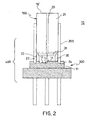
- Figures 1 and 2 show an optical apparatus 10 in accordance with a first embodiment of the invention.
- This optical apparatus 10 comprises a optical module 400 and means 100 of guided propagation of electromagnetic radiation.
- the optical module 400 includes an optoelectronic module or unit 300 provided, optionally, with a structure 200 for positioning the propagation means100. It should be observed that in agreement with the invention, with regards to production and trade it is possible to supply the optoelectronic unit 300 alone, not fixed to the structure of positioning 200 and not provided with propagation means 100. Alternatively, it is possible to market the optoelectronic unit 300 fixed to the support structure 200 and provided or not provided with the propagation means 100.
- the propagation means 100 include an optical wave guide such as, preferably, an optical fibre 20 and a ferrule or bushing 21 that, at least partially, houses the optical fibre itself.
- the optical fibre 20 is, for example, any conventional type fibre (monomodal or multimodal) and comprises a mantle, a nucleus or core and is devoid of external plastic coating.
- the optical fibre 20 is made of vitreous material (for example, silicon dioxide SiO2).
- the optical fibre 20 can have an external diameter of approximately 125 ⁇ m.
- the dimensions of the core are, for example, of 10 ⁇ m for monomodals, and of 50 ⁇ m (European standard) or 62.5 ⁇ m (American standard) for the multimodals.
- the ferrule 21 is made, for example, in zirconium or in steel and comprises a substantially cylindrical body that presents an internal channel, centred on the axis of the cylinder, destined to receive the optical fibre 20.
- the ferrule 21 can be of the same type as those associated to the fibre connectors on the market.
- the ferrule 21 presents a diameter of the internal channel of 125 ⁇ m and an external diameter of 2.5 mm.
- the ferrule 21 has a substantially truncated cone shape.
- the optical fibre 20 presents one end 19, suitably processed to reduce the reflection of optical radiation, aligned with a wall 19' of the ferrule itself.
- the positioning structure 200 consists, preferably, in a single sleeve such as to define an internal hollow region 22 suitable for housing the ferrule 21. This sleeve 200 is destined to be mechanically coupled to the support substrate 11.
- the sleeve 200 is, for example, of the type normally used for the connection of two ferrules and indicated in the sector by the English term "sleeve".
- This sleeve is, for example, the shape of a cylinder devoid of a longitudinal portion and is made, typically, in zirconium.
- the sleeve 200 is such as to present an elasticity that allows it to exert a grip force on the ferrule to which it is applied.
- the sleeve 200 performs the function of consenting the correct positioning and alignment of the propagation means 100 in relation to the optoelectronic unit 300.
- the sleeve 200 is applied to the ferrule 21 (which wraps around the optical fibre 20) such that one outer edge 23 of the sleeve itself is free and that is protruding in relation to the ferrule itself.
- figure 3 shows the optoelectronic unit 300 in greater detail.
- This optoelectronic unit 300 comprises a support substrate 11, an optoelectronic device 12 fixed to the substrate 11 and a reflection device 14 (i.e. a mirror) integrated into the substrate 11.
- the support substrate 11 is, preferably, in silicon, but other materials, such as, for example, glass or alumina may also be used.
- the support substrate 11 identifies an upper surface Sup and is provided with a fixing groove 24.
- the groove 24 (for example, with a rectangular or square section) is such to define in the substrate 11 a path that is, for example, semicircular and is destined to receive the free edge 23 of the sleeve 20.
- the depth L1 and width L2 of the groove 24 have values such to receive the edge 23 of the sleeve 200.
- a hollow region 25 having a bottom wall 26 that is, for example, aligned with the bottom wall of the groove 24.
- the reflection device 14 including a reflective surface 15. This reflective surface 15 stretches from the bottom wall 26 to the upper surface Sup.
- One particular embodiment of the reflection and focusing device 14 will be described in greater detail later.
- the optoelectronic device 12 is, for example, a semiconductor device. According to the first embodiment of the invention the optoelectronic device 12 is a laser.
- this laser 12 can be a conventional semiconductor laser.
- the laser 12 has a substantially parallelepiped shape and presents at least one principle output port or surface 13 of the electromagnetic radiation generated.
- this output port is positioned on one lateral face 27 of the laser 12 arranged in a transverse way and, in particular, perpendicular to the bottom wall 26 and facing towards the reflection device 14.
- the laser 12 presents the following dimensions: height equal to approximately 100 ⁇ m, length between 300-400 ⁇ m, width between 300-400 ⁇ m.
- the support substrate 11 is suitably fixed to a base 28 having the function of support and suitable for the dissipation of the heat produced by the laser 12.
- the base 28 shaped, for example, like a disk could be made in a metallic alloy such as, for example, the iron-cobalt-nickel alloy known by the name of Kovar, or it can be made in ceramic material.
- Rheophores 32 (for example, four rheophores) are inserted inside holes made in the base 28 in electrical contact with the support 11, for the supply of electrical voltage to the laser 12.
- the laser 12 in a lower portion, is provided with an upper electrical contact (not shown), for example, coinciding with a welding on the support 11 and, in an upper portion it is in turn connected to a lower electric contact in turn connected to a conductive wire ("bonding" wire, not shown).
- the optoelectronic unit 300 is also provided, advantageously, with a blockage structure 29 arranged on the upper surface Sup of the substrate 11 and destined to extend inside the sleeve 200 when it is mounted to the substrate itself.
- the blockage structure 29 makes it possible to block the ferrule 21 at the preset distance L from the upper surface Sup.
- the distance L chosen in such a way as to put the port 19 of the optical fibre 20 at a preset distance from the reflection device 14.
- the blockage structure 29 includes a tubular body 30 made, for example, in metallic material and fixed to a circular region of the upper surface Sup inside the area delimited by the sleeve 200.
- the blockage structure 29 is also provided with a window 31 that can be made, for example, in glass or plastic or with any other material substantially transparent to the wavelength of the radiation transmitted.
- a window is intended as a substantially transparent optical element made with a material having a substantially constant refraction index and having two opposite radiation input/output surfaces (that is two surfaces interfacing with the surrounding space) that are flat and parallel to one another.
- this window 31 has a disk shape and is applied to the upper edge of the tubular body 30 that acts as a support wall.
- this upper edge of the tubular body 30 is purposely shaped in order to favour geometric coupling with a crown of the window 31.
- the window 31 is fitted with a metal coating of its crown in such a way as to be fitted by welding to the edge of the tubular body 30.
- the blockage structure 29 can be made in a single block for example, in plastic, including the tubular body 30 and the window 31.
- the blockage structure 29 defines together with the support substrate 11 a cavity C inside which is housed the laser 12 and the reflection device 14.
- the optoelectronic unit 300 also includes a photodetection monitoring device such as, for example, a photodiode (not shown) having the function of monitoring the optical radiation generated by the laser 12.
- a photodetection monitoring device such as, for example, a photodiode (not shown) having the function of monitoring the optical radiation generated by the laser 12.
- This monitoring photodiode can be integrated into the substrate 11 or can be fixed on the upper surface Sup or in the cavity 25.
- the monitoring photodiode can detect optical radiation coming out from another port of the laser 12 which, according to the example described, is the radiation coming out of the wall of the laser opposite that 13 facing the reflection device 14.
- the monitoring photodiode can be arranged in such a way as to receive a part of the radiation that in any case is retroreflected from the window 31.
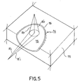
- the reflection device 14 includes the reflective wall 15 arranged above a concave base surface 19, formed in the substrate 11.
- the concave base surface 16 is a joining surface between the bottom wall 26 of the cavity 25 and the upper surface Sup of the substrate 11 or, in other words, it stretches two portions 11a and 11b of the substrate 11 having different thicknesses to one another.
- the reflective wall 15 is metallic and is obtained by a metalization of the concave base surface 16 of the substrate 11 with one or more metal layers, suitable for the reflection of radiation with optical wavelengths.
- the reflective wall aluminium gold, or, preferable silver, can be used.
- the coupling device 14 includes on the metallic reflective wall 15 at least one protective layer 15', for example in silicon dioxide, having the aim of preventing the oxidation of the reflective wall itself.
- the substrate 11 is constituted by a material such as, for example, gold, suitable for the reflection of optical electromagnetic radiation
- the metalization of the base surface 16 formed in the substrate 11 would not be necessary. In this case the reflective surface 15 and the base surface 16 would coincide.
- the reflective wall 15 is suitable for receiving an incident electromagnetic radiation, which in this example is the radiation coming out from the laser 12, in order to produce reflected electromagnetic radiation.
- the reflective wall 15 is such as to operate as a mirror.
- the radiation coming out from port 13 has approximately the pace of a Gaussian beam.
- the segments Ri and Ri' identify in each point, along the direction of propagation, the quantity that is known to a man skilled in the art with the name of divergence from the Gaussian beam.
- the reflective surface 15 is such that, with good approximation, the reflected radiation is confined within a reflective beam identified (in a qualitative way) by segments Rr and Rr'.
- the reflective wall 15 (in the same way as the base 16) defines a concave three-dimensional surface that is such that the profile of its two sections with planes parallel and perpendicular to any axis of propagation of the incident electromagnetic radiation is a concave curve.
- regular concave reflective surfaces that can be advantageously used for the reflection device 14 are listed below: portions of spherical, hyperbolic, ellipsoidal and parabolic surfaces, or more generally, portions of surfaces of the second order (quadric) or even of higher orders, with the aim of correcting any optical aberrations.
- the reflective wall 15 is designed in such a way as to generate a reflected electromagnetic radiation such as to be able to be coupled in the input port 19 of the optical fibre 20.
- the reflective surface 15 makes it possible to focus the incident electromagnetic radiation.
- the reflective surface 15 if struck by an incident radiation having a diverging transverse field intensity distribution generates a reflected electromagnetic radiation having a converging transverse electromagnetic field distribution intensity and vice versa.
- the reflected radiation is substantially confined within a beam with view angle ⁇ and that converges along the direction of propagation of the reflected radiation.
- the view angle of the reflected beam is equal to the numerical aperture of the optical fibre 20. In this way one makes an optimum coupling between the laser 12 and the optical fibre 20 that receives the reflected radiation.
- the laser 12 suitably powered by the rheophores 32 emits a diverging type optical beam.
- This optical beam strikes the concave reflective wall 15 which reflects and focuses it, thus making it a converging beam, suitable for reaching (through the window 30) the input port 19 of the optical fibre 20 and propagating inside the latter.
- the laser 12 and the optical fibre 20 are optically coupled without interposition of lenses, that is without interposition of optical elements such as to introduce important modifications to the characteristics of the optical beam in addition to those due to the reflection associated to the reflection device 14.
- laser 12 and the reflection device 14 are coupled with one another without interposition of lenses, and the device 14 and the optical fibre 20 are coupled to one another without interposition of lenses.
- optical apparatus 10 can provide a mechanical means of support for conferring greater sturdiness to the sleeve 200.
- Figures 6A and 6b show an example of such a mechanical means of support that materialises in an outer sleeve 500 in which at least part of the sleeve 200 and part of the tubular element 30 is inserted.
- the optical fibre 20 provided, optionally, with a plastic material coating can lead out. It should be observed that the use of the window 31 that also performs a role of closure of the hollow region in which the laser 12 is housed is particularly advantageous.
- the apparatus 10 when the apparatus 10 is such that the step of insertion of the ferrule 21 into the sleeve 200 is performed by the same user, and not in the manufacture phase, it is important to protect the cavity C that receives the laser 12 from contaminations.
- the optical fibre 20 is fixed to the ferrule 21 by glue and that the ferrule itself is fixed to the sleeve 200 once again by glue.
- the welding of the window 31 to the edge of the tubular body 30 is especially advantageous.
- the optical apparatus 10 is not provided with the window 31 but the outer wall 19' of the sleeve 200 is positioned, during manufacture, directly in contact with the upper edge of the tubular body 30.
- the optoelectronic device 12 is not a laser but is a photodetector or photoreceptor that can be applied, for example, to the bottom wall 26 in the same way as said for the laser 12.
- a photodetector suitable for being used in the apparatus of this invention is the detector known in the sector with the term pin detector.
- a photodetector of this type is marketed for example by Honeywell.
- This type of photodetector presents a substantially parallelepiped form and is provided with a portion destined to receive the optical radiation positioned on a lateral face of the parallelepiped.
- This face of the photodetector can be oriented in exactly the same way as shown in figures 1-3 for the laser 12, in order to receive the radiation reflected by the reflection and focusing device 14.
- the reflective wall 15 defines a concave surface suitable for collimating the incident electromagnetic radiation.
- the reflective wall 15 is such to produce, starting from an incident electromagnetic radiation having a diverging transverse distribution of field intensity, a reflective electromagnetic radiation having a transverse distribution of electromagnetic field intensity that substantially presents the characteristics of a collimated beam.
- a collimated beam presents a transverse distribution of field intensity approximately constant along the direction of propagation of the electromagnetic radiation.
- the reflective surface 15 has a parabolic profile and that the output interface 13 of optical radiation is arranged in focus of said surface.
- the fixing groove 24 can be obtained by conventional type photolithographic techniques.
- the forming process of the fixing groove 24 foresees the use of a mask, the deposition of a layer of photoresist and oxide on the surface Sup of the support substrate 11.
- this attachment is a chemical anisotropic attachment (which is known per se) that creates the fixing groove 24.
- Photolithographic techniques are also used to create in the support substrate 11 the hollow region 25 in which the laser 12 will be fixed.
- the formation of the hollow region 25 can be performed in completely the same way as the formation of the fixing groove 24 and foresees the use of a mask, the development of a layer of photoresist and a subsequent attachment of the substrate 11.
- the formation of the fixing groove 24 and of the hollow region 25 can take place by means of a single mask and a single attachment step of the substrate.
- the creation of the base surface 16 may, for example, entail the use of a gray scale mask that can be constituted by a plate of glass opacified by an electronic beam. This plate is opacified in order to record in it a gray scale correlated to the form desired for the base surface 16 and, in particular, corresponding to predetermined depths of level of attachment of a layer of photoresist.
- This gray scale mask is therefore used to expose a layer of photoresist, arranged on the upper surface Sup of the support substrate 11, to a suitable radiation.
- the layer of photoresist and the underlying support substrate 11 are attached in such a way as to remove portions of the substrate 11 of different depths, thus obtaining the base surface 16.
- This attachment can be, preferably, a chemically assisted "ion beam milling" ion beam type.
- phase mask for example, similar to those used in the manufacture of optical fibre lattice can be used.
- the manufacture process in accordance with the invention also includes a step of metalization for the formation of a metallic pad 33 (see figure 4 ) on which the laser 12 is fixed.
- This step of metalization can also be conducted using the photolithographic technique that foresees the formation of an aperture in a layer of oxide arranged on the bottom wall 26 inside which a metallic layer, for example, gold, is deposited.
- the laser 12 is fixed by welding to the pad thus obtained according to a conventional technique known with the term "die attach" of the laser.
- This welding step is of a conventional type and can lead to a precision of alignment of between 1 and 10 ⁇ m.
- the laser 12 is fixed to the pad positioned on the bottom wall 26 in such a way as to be correctly aligned with the reflection device 14.
- alignment signs useful for the correct orientation of the laser 12 on the pad itself may be made on the metallic pad.
- further signs destined to match with the signs formed on the pad 33 are formed on the lower wall of the laser 12.
- alignment signs are advantageous in the case of applications that require extreme precision in the alignment between the laser 12 and the reflection device 14.
- Such alignment signs have, for example, the form of crosses, lines, etc., and are made using a photolithographic technique to create an optical type contrast, visible using a microscope or a video camera.
- the blockage structure 29 is fixed to the upper surface Sup of the substrate 11.
- a lower edge of the tubular structure 30 is glued or welded to a region of the upper surface Sup inside an area that can be defined by the fixing groove 24.
- a gas such as, for example, nitrogen is inserted, until saturation, in order to create an inert atmosphere and avoid contamination of the laser 12.
- the method of the invention also foresees the fixing to the base 28, by a gluing or welding step , of a wall of the support substrate 11 opposite to the upper surface Sup.
- a step of fixing of the sleeve 200 to the support substrate 11 of the optoelectronic unit 300 forming the optical module 400 is then performed.
- this fixing takes place by arranging glue inside the fixing groove 24.
- the edge 23 of the sleeve 200 is placed inside the fixing groove 24 thus causing a redislocation of the glue, which may partially leak from the groove itself.
- the ferrule 21, provided with the optical fibre 20, is inserted into the cavity 22 of the sleeve 200 in such a way that its outside edge 19' (aligned with end 19 of the optical fibre 20) is brought into contact with an upper surface of the window 31.
- optical apparatus 10 of the present invention presents considerable advantages over the state of the art apparatus.
- this optical apparatus 10 and the optical module 400 ensure a good coupling efficiency between the optical fibre 20 and the optoelectronic device 12.
- the apparatus of the invention presents the reflection device 14 integrated, preferably, by a photolithographic technique, in the same support substrate 11 on which the optoelectronic device 12 (be it a laser or a photodetector)is fixed. Therefore, the correct positioning of the reflection device 14 is based on a photolithographic type process that ensures high precision.
- the positioning of the sleeve 200, used for the fixing of the ferrule 21 containing the optical fibre 20, can be performed with high precision because it takes place by means of the groove 24, which can also be obtained by a photolithographic process.
- optical components of the apparatus 10 can also be obtained because the same optoelectronic device 12 can be fixed to the support substrate 11 with the aid of photolithographic techniques (for the formation of the fixing pad or for the formation of signs useful for orientation).
- optical apparatus of the invention not necessarily requiring the use of optical lenses, also makes it possible to reduce the cost of production in relation to conventional modules. In addition, it presents a limited number of optical components to align, thus making the operation of apparatus assembly uncomplicated.
Landscapes
- Physics & Mathematics (AREA)
- General Physics & Mathematics (AREA)
- Optics & Photonics (AREA)
- Optical Couplings Of Light Guides (AREA)
Claims (27)
- Optisches Modul (400), das folgende Merkmale aufweist:a) ein optoelektronisches Bauteil (12), das ein Tor für elektromagnetische Strahlung aufweist;b) ein Stützsubstrat (11), an dem das optoelektronische Bauteil befestigt ist und das eine obere Oberfläche (SUP) definiert, die mit einer hohlen Region (25) versehen ist, die eine untere Wand (26) aufweist;c) ein Reflexionsbauteil (14), das dazu geeignet ist, auftreffende Strahlung zu empfangen und reflektierte Strahlung zu erzeugen, und in eine laterale wand (16) der hohlen Region (25) in einer derartigen Weise integriert ist, um in einen optischen Pfad zwischen dem optoelektronischen Bauteil (12) und einer externen Ausbreitungseinrichtung (100) eingefügt zu sein, wobei eine optische Kopplung zueinander ermöglicht wird; wobei das Tor zu dem Reflexionsbauteil (14) hin gewandt ist;d) eine Buchse (200), die von dem Substrat abgesondert ist, um zum Stützen und Häusen der externen Ausbreitungseinrichtung (100) eingesetzt zu werden;
ferner durch folgende Merkmale gekennzeichnet:e) eine Befestigungsanschlussfläche (33), die an der unteren Wand (26) platziert ist und an der das optoelektronische Bauteil (12) befestigt ist; wobei das Tor an einer Seite des optoelektronischen Bauteils quer zu der unteren Wand (26) angeordnet ist;f) eine Befestigungsrille (24), die in dem Substrat (11) gebildet ist, wobei die Rille (24) angeordnet ist, um die freie Kante (23) der Buchse (200) zu empfangen; wobei die hohle Region (25) eine untere Wand (26) aufweist, die in einem Bereich der oberen Oberfläche (SUP) angeordnet ist, der durch die Rille (24) begrenzt ist; und wobei die Buchse (200) sich senkrecht zu der oberen Oberfläche (SUP) erstreckt. - Das Modul (400) gemäß Anspruch 1, bei dem das Reflexionsbauteil (14) eine konkave reflektierende Wand (15) umfasst.
- Das Modul (400) gemäß Anspruch 1, bei dem das Modul und das Reflexionsbauteil (14) derart sind, um optisch mit der externen Ausbreitungseinrichtung (100) ohne ein Dazwischenliegen von Linsen gekoppelt zu sein.
- Das Modul (400) gemäß Anspruch 1, bei dem das Reflexionsbauteil (14) und das optoelektronische Bauteil (12) optisch ohne ein Dazwischenliegen von Linsen gekoppelt sind.
- Das Modul (400) gemäß Anspruch 1, bei dem die externe Ausbreitungseinrichtung (100) eine optische Faser (20) umfasst.
- Das Modul (400) gemäß Anspruch 5, bei dem die externe Ausbreitungseinrichtung eine Hülse (21) umfasst, die extern an der optischen Faser (20) befestigt sein kann.
- Das Modul (400) gemäß Anspruch 1, das zusätzlich eine Blockierungsstruktur (29) aufweist, die einen Abschnitt aufweist, der dazu geeignet ist, in einem direkten Kontakt mit einem Ende (19') der externen Ausbreitungseinrichtung (100) positioniert zu sein, um dieselbe in einem voreingestellten Abstand von dem Reflexionsbauteil (14) zu blocken.
- Das Modul (400) gemäß Anspruch 7, bei dem die Blockierungsstruktur (29) folgende Merkmale umfasst:- zumindest eine Stützwand (30), die an dem Stützsubstrat (11) befestigt ist,- ein optisches Fenster (31), das an der Stützwand befestigt ist und in einer derartigen Weise angeordnet ist, um die optische Kopplung zwischen der Ausbreitungseinrichtung und dem Reflexionsbauteil (14) ohne ein Dazwischenliegen von Linsen zu ermöglichen; wobei das optische Fenster, die Stützwand und eine Oberfläche des Stützsubstrats (26, Sup) einen Hohlraum (C) definieren, in dem das optoelektronische Bauteil (12) gehäust ist.
- Das Modul (400) gemäß Anspruch 2, bei dem die konkave reflektierende Wand (15) derart ist, um die auftreffende elektromagnetische Strahlung in einer derartigen Weise zu fokussieren, um, von einer auftreffenden elektromagnetischen Strahlung beginnend, die eine divergierende Querverteilung einer Feldstärke aufweist, eine reflektierte elektromagnetische Strahlung zu erzeugen, die eine konvergierende Querverteilung einer Feldstärke aufweist.
- Das Modul (400) gemäß Anspruch 2, bei dem die konkave reflektierende Wand (15) derart ist, um die auftreffende elektromagnetische Strahlung in einer derartigen Weise zu kollimieren, um, von einer auftreffenden elektromagnetischen Strahlung beginnend, die eine divergierende Querverteilung einer Feldstärke aufweist, eine reflektierte elektromagnetische Strahlung zu erzeugen, die eine kollimierte Querverteilung einer Feldstärke aufweist.
- Das Modul (400) gemäß Anspruch 2, bei dem die reflektierende Wand (15) zumindest einen Abschnitt einer der folgenden Oberflächen definiert: sphärische, hyperbolische, ellipsoidische, parabolische Oberfläche.
- Das Modul (400) gemäß Anspruch 2, bei dem die reflektierende Wand (15) über einer konkaven Basisoberfläche (16) angeordnet ist, die in dem Substrat (11) gebildet ist.
- Das Modul (400) gemäß Anspruch 12, bei dem die BasisOberfläche (16) eine Verbindungsoberfläche von zwei freien Oberflächen (11a, 11b) ist, die zu Abschnitten des Substrats (11) mit zueinander unterschiedlichen Dicken gehören.
- Das Modul (400) gemäß Anspruch 2, bei dem die reflektierende Wand (15) eine Schicht aus einem metallischen Material umfasst.
- Das Modul (400) gemäß Anspruch 2, bei dem das Reflexionsbauteil (14) eine Schicht aus einem Schutzmaterial zum Verhindern der Oxidation der reflektierenden Wand (15) umfasst.
- Das Modul (400) gemäß Anspruch 1, bei dem das optoelektronische Bauteil (12) ein Laser zur Erzeugung von optischer Strahlung ist, die an die externe Ausbreitungseinrichtung (100) durch eine Reflexion auf dem Reflexionsbauteil (14) gesendet werden soll.
- Das Modul (400) gemäß Anspruch 16, bei dem der Laser vom Halbleitertyp ist.
- Das Modul (400) gemäß Anspruch 1, bei dem das optoelektronische Bauteil (12) ein Photodetektor zum Empfangen von optischer Strahlung ist, die durch das Reflexionsbauteil (14) reflektiert wird und aus der externen Ausbreitungseinrichtung (100) austritt.
- Das Modul (400) gemäß Anspruch 1, bei dem die Befestigungsanschlussfläche metallisch ist und das optoelektronische Bauteil (12) an die metallische Befestigungsanschlussfläche geschweißt ist.
- Das Modul (400) gemäß Anspruch 1, das zusätzlich eine Basis (28) umfasst, an der das Stützsubstrat (11) und Rheophoren (32), die elektrisch mit dem optoelektronischen Bauteil (12) verbunden sind, befestigt sind.
- Das Modul (400) gemäß Anspruch 1, bei dem die Buchse (200) zylindrisch ist.
- Eine optische Vorrichtung (10), die ein optisches Modul (400) aufweist, das ein optoelektronisches Bauteil (12) und eine geführte Ausbreitungseinrichtung einer elektromagnetischen Strahlung (100) umfasst, die dazu bestimmt ist, optisch mit dem optoelektronischen Bauteil (12) gekoppelt zu sein, durch die Tatsache gekennzeichnet, dass das optische Modul (400) gemäß zumindest einem der vorhergehenden Ansprüche ist.
- Verfahren zum Herstellen einer optischen Vorrichtung (10), die mit einem optoelektronischen Bauteil (12) versehen ist, das optisch mit der geführten Ausbreitungseinrichtung (100) einer optischen Strahlung gekoppelt werden soll, wobei das verfahren den Schritt eines Lieferns des optischen Moduls (400) gemäß zumindest einem der Ansprüche 1 bis 21 umfasst; wobei das Reflexionsbauteil (14) durch eine photolithographische Technik in das Stützsubstrat (11) integriert wird.
- Das Verfahren gemäß Anspruch 23, bei dem der Schritt des Lieferns des optischen Moduls folgende Schritte umfasst:- Bilden der Befestigungsrille (24) in dem Stützsubstrat mittels einer photolithographischen Technik,- Einfügen eines freien Abschnitts der Buchse (200) in die Befestigungsrille, um die Buchse an dem Stützsubstrat zu befestigen.
- Das verfahren gemäß Anspruch 23, bei dem der Schritt des Lieferns des Moduls ferner einen Schritt eines Befestigens des optoelektronischen Bauteils an dem Stützsubstrat (11) aufweist, mit folgenden Schritten:- Bilden der Befestigungsanschlussfläche (33) auf dem Stützsubstrat (11) mittels einer photolithographischen Technik,- Befestigen des optoelektronischen Bauteils (12) an der Befestigungsanschlussfläche (33) in einer derartigen Weise, um dasselbe mit dem Reflexionsbauteil optisch zu koppeln.
- Das Verfahren gemäß Anspruch 25, das zusätzlich den Schritt eines Bildens von zeichen an der Befestigungsanschlussfläche (33) und/oder an einer Wand des optoelektronischen Bauteils (12) aufweist, die für die korrekte Ausrichtung des optoelektronischen Bauteils (12) nützlich sind.
- Das Verfahren gemäß Anspruch 23, bei dem die Integration des Reflexionsbauteils in das Stützsubstrat (11) folgende Schritte umfasst:- Liefern einer Grauskalenmaske, die mit der Form der konkaven reflektierenden Wand (15) korreliert wird, die erhalten werden muss,- Anordnen einer Schicht aus Photoresist auf dem Stützsubstrat (11) und Umgeben einer derartigen Schicht aus Photoresist mit elektromagnetischer Strahlung, die die Grauskalenmaske kreuzt,- Durchführen eines Schrittes einer Anlagerung, um die Schicht aus Photoresist und Abschnitte des Stützsubstrats (11) in einer derartigen Weise zu entfernen, um die konkave Oberfläche (16) zu erhalten, die der reflektierenden Wand (15) entspricht.
Priority Applications (3)
| Application Number | Priority Date | Filing Date | Title |
|---|---|---|---|
| EP03425823A EP1548473B1 (de) | 2003-12-24 | 2003-12-24 | Optisches Modul mit einer optoelektronischen Einrichtung und einer reflektierenden optischen Kupplungsvorrichtung |
| DE60321583T DE60321583D1 (de) | 2003-12-24 | 2003-12-24 | Optisches Modul mit einer optoelektronischen Einrichtung und einer reflektierenden optischen Kupplungsvorrichtung |
| US11/015,363 US7223024B2 (en) | 2003-12-24 | 2004-12-17 | Optical module including an optoelectronic device |
Applications Claiming Priority (1)
| Application Number | Priority Date | Filing Date | Title |
|---|---|---|---|
| EP03425823A EP1548473B1 (de) | 2003-12-24 | 2003-12-24 | Optisches Modul mit einer optoelektronischen Einrichtung und einer reflektierenden optischen Kupplungsvorrichtung |
Publications (2)
| Publication Number | Publication Date |
|---|---|
| EP1548473A1 EP1548473A1 (de) | 2005-06-29 |
| EP1548473B1 true EP1548473B1 (de) | 2008-06-11 |
Family
ID=34530878
Family Applications (1)
| Application Number | Title | Priority Date | Filing Date |
|---|---|---|---|
| EP03425823A Expired - Lifetime EP1548473B1 (de) | 2003-12-24 | 2003-12-24 | Optisches Modul mit einer optoelektronischen Einrichtung und einer reflektierenden optischen Kupplungsvorrichtung |
Country Status (3)
| Country | Link |
|---|---|
| US (1) | US7223024B2 (de) |
| EP (1) | EP1548473B1 (de) |
| DE (1) | DE60321583D1 (de) |
Families Citing this family (9)
| Publication number | Priority date | Publication date | Assignee | Title |
|---|---|---|---|---|
| DE102005059524A1 (de) * | 2005-09-30 | 2007-04-05 | Osram Opto Semiconductors Gmbh | Gehäuse für ein elektromagnetische Strahlung emittierendes optoelektronisches Bauelement, Bauelement und Verfahren zum Herstellen eines Gehäuses oder eines Bauelements |
| KR101132680B1 (ko) | 2010-03-19 | 2012-04-03 | 김영혜 | 광전소자 패키지 |
| US8488921B2 (en) * | 2010-07-16 | 2013-07-16 | International Business Machines Corporation | Packaged multicore fiber optical transceiver module |
| EP2633350A1 (de) * | 2010-10-26 | 2013-09-04 | Biolase Technology, Inc. | Kollimierungskoppler für laserbehandlungsvorrichtungen |
| WO2014004375A1 (en) * | 2012-06-25 | 2014-01-03 | Quantum Electro Opto Systems Sdn. Bhd. | Method and apparatus for aligning of opto-electronic components |
| US10033464B2 (en) | 2013-05-28 | 2018-07-24 | Stmicroelectronics S.R.L. | Optoelectronic device having improved optical coupling |
| US20150147034A1 (en) * | 2013-11-27 | 2015-05-28 | Texas Instruments Incorporated | Optical Connector |
| JP6664255B2 (ja) * | 2016-03-29 | 2020-03-13 | ホシデン株式会社 | 光ファイバアレイと光モジュールとの接続構造 |
| KR20170138169A (ko) * | 2016-06-07 | 2017-12-15 | 한국과학기술원 | V자 구조 또는 곡면 구조의 반사체를 이용한 광 패키지 및 그 제작 방법 |
Family Cites Families (6)
| Publication number | Priority date | Publication date | Assignee | Title |
|---|---|---|---|---|
| US4699453A (en) * | 1982-11-24 | 1987-10-13 | Magnetic Controls Company | Monolithic fiber optic coupler having total internal reflecting surface |
| JPS62106686A (ja) * | 1985-11-01 | 1987-05-18 | Matsushita Electric Ind Co Ltd | 半導体レ−ザ装置 |
| WO1996022177A1 (de) * | 1995-01-18 | 1996-07-25 | Robert Bosch Gmbh | Anordnung zur umsetzung von optischen in elektrische signale und verfahren zur herstellung |
| KR100272265B1 (ko) * | 1996-12-30 | 2000-12-01 | 김영환 | 광통신 모듈용 파이버 피그테일 |
| US20030099273A1 (en) * | 2001-01-09 | 2003-05-29 | Murry Stefan J. | Method and apparatus for coupling a surface-emitting laser to an external device |
| US6786651B2 (en) * | 2001-03-22 | 2004-09-07 | Primarion, Inc. | Optical interconnect structure, system and transceiver including the structure, and method of forming the same |
-
2003
- 2003-12-24 EP EP03425823A patent/EP1548473B1/de not_active Expired - Lifetime
- 2003-12-24 DE DE60321583T patent/DE60321583D1/de not_active Expired - Lifetime
-
2004
- 2004-12-17 US US11/015,363 patent/US7223024B2/en not_active Expired - Lifetime
Also Published As
| Publication number | Publication date |
|---|---|
| US7223024B2 (en) | 2007-05-29 |
| US20050163435A1 (en) | 2005-07-28 |
| DE60321583D1 (de) | 2008-07-24 |
| EP1548473A1 (de) | 2005-06-29 |
Similar Documents
| Publication | Publication Date | Title |
|---|---|---|
| US6205274B1 (en) | Fiber optic header for an edge emitting laser | |
| US20220026649A1 (en) | Optical connection of optical fibers to grating couplers | |
| US6081638A (en) | Fiber optic header with integrated power monitor | |
| US6567435B1 (en) | VCSEL power monitoring system using plastic encapsulation techniques | |
| US5526455A (en) | Connector including opposing lens surfaces, side surfaces, and contact surfaces for coupling optical devices | |
| US8827572B2 (en) | Side coupling optical fiber assembly and fabrication method thereof | |
| US9897769B2 (en) | Vision-based passive alignment of an optical fiber subassembly to an optoelectronic device | |
| CN104364689B (zh) | 用于耦合光纤输入/输出的具有结构化反射表面的耦合装置 | |
| US7404679B2 (en) | Termination for optic fiber with improved optical features | |
| AU2015258871B2 (en) | Optical connection of optical fibers to grating couplers | |
| US7137745B2 (en) | Subassembly and optical module | |
| JPH1082930A (ja) | 光モジュール,およびその製造方法 | |
| JP2006072232A (ja) | 光送受信モジュール | |
| JP4809353B2 (ja) | マイクロマシン構造体に気密パッケージされた光学モジュール | |
| EP1548473A1 (de) | Optisches Modul mit einer optoelektronischen Einrichtung und einer reflektierenden optischen Kupplungsvorrichtung | |
| EP2778730B1 (de) | Optische unterbaugruppe und verfahren zu seiner herstellung | |
| TW463063B (en) | Optical module | |
| US7850374B2 (en) | Optical transmitter module with an integrated lens and method for making the module | |
| JP2004095824A (ja) | 発光モジュール | |
| US6243524B1 (en) | Optical waveguide, method for fabricating same, and coupling structure of optical waveguide to light-receiving device | |
| JP2003520353A (ja) | マルチファイバアレー用光電子モジュール | |
| WO2010128327A1 (en) | Optical collimator and light collection assembly having a concave reflecting surface | |
| JP4770551B2 (ja) | 光モジュール | |
| JPH0496390A (ja) | 光通信用パッケージ | |
| JP3779049B2 (ja) | 光モジュールとその製造方法、並びに、光学的反射部材とその位置決め方法及び装置 |
Legal Events
| Date | Code | Title | Description |
|---|---|---|---|
| PUAI | Public reference made under article 153(3) epc to a published international application that has entered the european phase |
Free format text: ORIGINAL CODE: 0009012 |
|
| AK | Designated contracting states |
Kind code of ref document: A1 Designated state(s): AT BE BG CH CY CZ DE DK EE ES FI FR GB GR HU IE IT LI LU MC NL PT RO SE SI SK TR |
|
| AX | Request for extension of the european patent |
Extension state: AL LT LV MK |
|
| 17P | Request for examination filed |
Effective date: 20051213 |
|
| AKX | Designation fees paid |
Designated state(s): DE FR GB IT |
|
| 17Q | First examination report despatched |
Effective date: 20060125 |
|
| GRAP | Despatch of communication of intention to grant a patent |
Free format text: ORIGINAL CODE: EPIDOSNIGR1 |
|
| GRAS | Grant fee paid |
Free format text: ORIGINAL CODE: EPIDOSNIGR3 |
|
| GRAA | (expected) grant |
Free format text: ORIGINAL CODE: 0009210 |
|
| AK | Designated contracting states |
Kind code of ref document: B1 Designated state(s): DE FR GB IT |
|
| REG | Reference to a national code |
Ref country code: GB Ref legal event code: FG4D |
|
| REF | Corresponds to: |
Ref document number: 60321583 Country of ref document: DE Date of ref document: 20080724 Kind code of ref document: P |
|
| PLBE | No opposition filed within time limit |
Free format text: ORIGINAL CODE: 0009261 |
|
| STAA | Information on the status of an ep patent application or granted ep patent |
Free format text: STATUS: NO OPPOSITION FILED WITHIN TIME LIMIT |
|
| 26N | No opposition filed |
Effective date: 20090312 |
|
| REG | Reference to a national code |
Ref country code: FR Ref legal event code: ST Effective date: 20090831 |
|
| PG25 | Lapsed in a contracting state [announced via postgrant information from national office to epo] |
Ref country code: FR Free format text: LAPSE BECAUSE OF NON-PAYMENT OF DUE FEES Effective date: 20081231 |
|
| PGFP | Annual fee paid to national office [announced via postgrant information from national office to epo] |
Ref country code: GB Payment date: 20101201 Year of fee payment: 8 |
|
| GBPC | Gb: european patent ceased through non-payment of renewal fee |
Effective date: 20121224 |
|
| PG25 | Lapsed in a contracting state [announced via postgrant information from national office to epo] |
Ref country code: GB Free format text: LAPSE BECAUSE OF NON-PAYMENT OF DUE FEES Effective date: 20121224 |
|
| PGFP | Annual fee paid to national office [announced via postgrant information from national office to epo] |
Ref country code: DE Payment date: 20131121 Year of fee payment: 11 |
|
| PG25 | Lapsed in a contracting state [announced via postgrant information from national office to epo] |
Ref country code: IT Free format text: LAPSE BECAUSE OF NON-PAYMENT OF DUE FEES Effective date: 20091224 |
|
| REG | Reference to a national code |
Ref country code: DE Ref legal event code: R119 Ref document number: 60321583 Country of ref document: DE |
|
| PG25 | Lapsed in a contracting state [announced via postgrant information from national office to epo] |
Ref country code: DE Free format text: LAPSE BECAUSE OF NON-PAYMENT OF DUE FEES Effective date: 20150701 |