EP1545180A2 - Wärmeleitende Einlegematte für elektrische und elektronische Geräte und Verfahren zur Herstellung derartiger Einlegematten - Google Patents
Wärmeleitende Einlegematte für elektrische und elektronische Geräte und Verfahren zur Herstellung derartiger Einlegematten Download PDFInfo
- Publication number
- EP1545180A2 EP1545180A2 EP04027142A EP04027142A EP1545180A2 EP 1545180 A2 EP1545180 A2 EP 1545180A2 EP 04027142 A EP04027142 A EP 04027142A EP 04027142 A EP04027142 A EP 04027142A EP 1545180 A2 EP1545180 A2 EP 1545180A2
- Authority
- EP
- European Patent Office
- Prior art keywords
- mat
- insert
- housing
- electrical
- mats
- Prior art date
- Legal status (The legal status is an assumption and is not a legal conclusion. Google has not performed a legal analysis and makes no representation as to the accuracy of the status listed.)
- Withdrawn
Links
Images
Classifications
-
- H—ELECTRICITY
- H05—ELECTRIC TECHNIQUES NOT OTHERWISE PROVIDED FOR
- H05K—PRINTED CIRCUITS; CASINGS OR CONSTRUCTIONAL DETAILS OF ELECTRIC APPARATUS; MANUFACTURE OF ASSEMBLAGES OF ELECTRICAL COMPONENTS
- H05K7/00—Constructional details common to different types of electric apparatus
- H05K7/20—Modifications to facilitate cooling, ventilating, or heating
- H05K7/2039—Modifications to facilitate cooling, ventilating, or heating characterised by the heat transfer by conduction from the heat generating element to a dissipating body
- H05K7/20436—Inner thermal coupling elements in heat dissipating housings, e.g. protrusions or depressions integrally formed in the housing
- H05K7/20445—Inner thermal coupling elements in heat dissipating housings, e.g. protrusions or depressions integrally formed in the housing the coupling element being an additional piece, e.g. thermal standoff
-
- H—ELECTRICITY
- H10—SEMICONDUCTOR DEVICES; ELECTRIC SOLID-STATE DEVICES NOT OTHERWISE PROVIDED FOR
- H10W—GENERIC PACKAGES, INTERCONNECTIONS, CONNECTORS OR OTHER CONSTRUCTIONAL DETAILS OF DEVICES COVERED BY CLASS H10
- H10W40/00—Arrangements for thermal protection or thermal control
- H10W40/20—Arrangements for cooling
- H10W40/25—Arrangements for cooling characterised by their materials
- H10W40/251—Organics
-
- H—ELECTRICITY
- H10—SEMICONDUCTOR DEVICES; ELECTRIC SOLID-STATE DEVICES NOT OTHERWISE PROVIDED FOR
- H10W—GENERIC PACKAGES, INTERCONNECTIONS, CONNECTORS OR OTHER CONSTRUCTIONAL DETAILS OF DEVICES COVERED BY CLASS H10
- H10W70/00—Package substrates; Interposers; Redistribution layers [RDL]
- H10W70/01—Manufacture or treatment
- H10W70/02—Manufacture or treatment of conductive package substrates serving as an interconnection, e.g. of metal plates
Definitions
- the invention relates to a method for producing thermally conductive insert mats for electrical and electronic equipment according to the preamble of the claim 1 and heat-conducting insert mats according to the preamble of patent claim 3 and control gear for electric lamps with such mats.
- the published patent EP 0 986 292 A2 discloses a thermally conductive insert mat for electrical and electronic equipment consisting of a modified hydrocarbon resin or consists of a silicone composite film. These mats are deformable, flexible and have a soft and sticky consistency.
- the Insert mats are made from a potting compound that is poured into molds and then under vacuum and heat for about eight hours is cured. The cost of these mats are due to the time-consuming Manufacturing process and the large number of required molds for the mats of different dimensions high.
- the heat-conductive insert mats for electrical and electronic Devices made of an electrically insulating, thermally conductive plastic produced by extrusion by means of an extruder.
- This procedure allows in Contrary to the manufacturing method according to the prior art, a cost-effective Mass production of the mats.
- the shape of the mats is through determines the shape of the outlet nozzle opening of the extruder and can therefore without great effort to be adapted to the desired application.
- No casting molds are required as in the manufacturing process according to the State of the art.
- thermally conductive mats all thermoplastic, thermally conductive plastics are used. Especially advantageous However, such plastics are in addition to a high thermal conductivity also allow a good electrical insulation.
- the mats according to the preferred embodiment therefore consist of silicone.
- the insert mats according to the invention advantageously have a flat underside and a longitudinal trough provided on top.
- the flat bottom allows one good thermal coupling to a housing wall of an electrical device while the louvers on the top, which delimit the longitudinal grooves, are different Clear the gaps between the housing wall and the heat source can, because the lamellae are flexible and flexible.
- the slats can be hollow to increase flexibility.
- a preferred field of application for the thermally conductive insertable mats according to the invention are factory baton for electric lamps. Own this operating device usually a housing and disposed within the housing electronic Components for the operation of lamps. To those generated by the electronic components Heat to dissipate through the housing better is between the electronic Components and the housing at least one of the insertion mats according to the invention arranged.
- the electronic components of the operating device are preferably fixed on a mounting board, which is at a short distance to a housing wall, is arranged for example to the bottom of the operating device.
- An inventive Insert mat is advantageous between the mounting board and the aforementioned Housing wall of the control gear arranged to a good thermal To obtain coupling between the electronic components and this housing wall.
- To further improve the heat dissipation can by means of the insert mat thermally coupled to the mounting board housing wall formed as a heat sink be, for example, by a sheet of metal or with a metal sheet is provided.
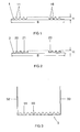
- FIG. 1 shows a first exemplary embodiment of the insertion mat according to the invention shown schematically.
- This insert mat 1 is made of silicone and has a Width B of 80 mm and a thickness H of 5 mm.
- the bottom of the insert mat 1 is flat, while its upper side with a plurality of longitudinal grooves 10th is provided, which have a depth of 4 mm.
- the longitudinal grooves 10 are laterally bounded by fins 11.
- the insert mat 1 is flexible and flexible.
- FIG. 2 shows a second embodiment of the insert mat according to the invention in a schematic representation.
- This insert mat 2 is made of silicone and has a width B of 80 mm and a thickness H of 5 mm.
- the bottom of the Lying mat 2 is flat, while its top with a variety of Longitudinal channels 20 is provided, which have a depth of 4 mm.
- the longitudinal channels 20 are bounded laterally by hollow blades 21.
- the insert mat 2 is flexible and flexible.
- FIG. 3 shows a third exemplary embodiment of the insert mat according to the invention shown schematically.
- This insert mat 3 is also made of silicone.
- the bottom of the insert mat 3 is flat, while its top with a plurality of longitudinal grooves 30 having a depth of 4 mm.
- the longitudinal grooves 30 are bounded laterally by fins 31.
- the thickness of the mat 3 is 5 mm.
- the insert mat 3 respectively a longitudinally extending, integrally formed side wall 32 and 33, respectively.
- the Lying mat 3 is flexible and flexible. This insert mat 3 allows a thermal Coupling to the ground and two side walls of the housing of an electric Device as well as an electrical insulation of the components.
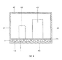
- FIG 4 is a cross section through an operating device for electric lamps shown schematically.
- the operating device has a substantially cuboidal Housing with a bottom 40, two side walls 41, 42, a cover 43rd and two end-side sidewalls (not shown). Inside the case are arranged on a mounting board 44, electronic components 45 arranged to the Operation of one or more electric lamps serve.
- the mounting board 44 is arranged at a distance of about 5 mm above the bottom 40.
- Figure 1 illustrated insert mat 1 In the space between the bottom 40 and the mounting board 44 is located in Figure 1 illustrated insert mat 1.
- the flat bottom of the insert mat 1 lies on the bottom 40, while provided with the longitudinal grooves 10 and fins 11 Top is in contact with the mounting board.
Landscapes
- Physics & Mathematics (AREA)
- Thermal Sciences (AREA)
- Engineering & Computer Science (AREA)
- Microelectronics & Electronic Packaging (AREA)
- Extrusion Moulding Of Plastics Or The Like (AREA)
- Cooling Or The Like Of Semiconductors Or Solid State Devices (AREA)
- Cooling Or The Like Of Electrical Apparatus (AREA)
Abstract
Description
- Figur 1
- Eine Seitenansicht eines ersten Ausführungsbeispiels der erfindungsgemäßen Einlegematte
- Figur 2
- Eine Seitenansicht eines zweiten Ausführungsbeispiels der erfindungsgemäßen Einlegematte
- Figur 3
- Eine Seitenansicht eines dritten Ausführungsbeispiels der erfindungsgemäßen Einlegematte
- Figur 4
- Einen Querschnitt durch ein Betriebsgerät für elektrische Lampen
Claims (7)
- Verfahren zur Herstellung einer wärmeleitenden Einlegematte, dadurch gekennzeichnet, dass die Einlegematte (1) aus einem wärmeleitenden Kunststoff durch Strangpressen mittels eines Extruders hergestellt wird.
- Verfahren nach Anspruch 1, dadurch gekennzeichnet, dass der wärmeleitende Kunststoff Silikon ist.
- Wärmeleitende Einlegematte für elektrische oder elektronische Geräte, dadurch gekennzeichnet, dass die Einlegematte (1) als Kunststoff-Strangpress-Profil ausgebildet ist.
- Einlegematte nach Anspruch 3, dadurch gekennzeichnet, dass die Einlegematte (1) aus einem elektrisch isolierenden Kunststoff besteht.
- Einlegematte nach Anspruch 3, dadurch gekennzeichnet, dass die Einlegematte (1) eine ebene Unterseite und eine mit Längsrinnen (10) versehene Oberseite besitzt.
- Einlegematte nach Anspruch 5, dadurch gekennzeichnet, dass die die Längsrinnen (10) begrenzenden Lamellen (11) hohl sind.
- Betriebsgerät für elektrische Lampen mit einem Gehäuse, innerhalb des Gehäuses (40, 41, 42, 43) angeordneten elektronischen Bauteilen (45) und mindestens einer zwischen den elektronischen Bauteilen (45) und dem Gehäuse (40, 41, 42, 43) angeordneten Einlegematte (1) gemäß eines oder mehrerer der vorstehenden Ansprüche.
Applications Claiming Priority (2)
| Application Number | Priority Date | Filing Date | Title |
|---|---|---|---|
| DE10359157A DE10359157A1 (de) | 2003-12-16 | 2003-12-16 | Wärmeleitende Einlegematte für elektrische und elektronische Geräte und Verfahren zur Herstellung derartiger Einlegematten |
| DE10359157 | 2003-12-16 |
Publications (2)
| Publication Number | Publication Date |
|---|---|
| EP1545180A2 true EP1545180A2 (de) | 2005-06-22 |
| EP1545180A3 EP1545180A3 (de) | 2008-03-05 |
Family
ID=34485428
Family Applications (1)
| Application Number | Title | Priority Date | Filing Date |
|---|---|---|---|
| EP04027142A Withdrawn EP1545180A3 (de) | 2003-12-16 | 2004-11-15 | Wärmeleitende Einlegematte für elektrische und elektronische Geräte und Verfahren zur Herstellung derartiger Einlegematten |
Country Status (2)
| Country | Link |
|---|---|
| EP (1) | EP1545180A3 (de) |
| DE (1) | DE10359157A1 (de) |
Cited By (2)
| Publication number | Priority date | Publication date | Assignee | Title |
|---|---|---|---|---|
| EP2442630A1 (de) * | 2010-10-18 | 2012-04-18 | Siemens Aktiengesellschaft | Wärmeleitpad |
| WO2012080827A3 (en) * | 2010-12-17 | 2012-08-30 | Eaton Corporation | Electrical system and matrix assembly therefor |
Families Citing this family (4)
| Publication number | Priority date | Publication date | Assignee | Title |
|---|---|---|---|---|
| DE202006007475U1 (de) * | 2006-05-09 | 2007-09-13 | ICOS Gesellschaft für Industrielle Communications-Systeme mbH | Schalteranordnung für Kommunikations-Datenströme, Schaltermodul für eine derartige Schalteranordnung sowie Kühlanordnung hierfür |
| DE102008047649B4 (de) | 2008-09-15 | 2011-03-31 | Gerhard Menninga | Platte zum Ausgleichen von Wärme in einer Leiterplatte und zum Abführen von Wärme von einer Leiterplatte und Anordnung einer solchen Platte mit einer Leiterplatte |
| DE202008012361U1 (de) | 2008-09-15 | 2012-12-14 | Gerhard Menninga | Platte und Anordnung zum Ausgleichen von Wärme in einer Leiterplatte und Abführen von Wärme von der Leiterplatte und von auf der Leiterplatte befindlichen Elementen |
| DE102016220877A1 (de) * | 2016-10-24 | 2018-04-26 | Volkswagen Aktiengesellschaft | Wärmeleitmatte, Batteriebaugruppe mit einer derartigen Wärmeleitmatte sowie Fahrzeug |
Family Cites Families (5)
| Publication number | Priority date | Publication date | Assignee | Title |
|---|---|---|---|---|
| US4654754A (en) * | 1982-11-02 | 1987-03-31 | Fairchild Weston Systems, Inc. | Thermal link |
| JP3372462B2 (ja) * | 1997-11-27 | 2003-02-04 | 電気化学工業株式会社 | ゴムシートの製造方法 |
| ATE324025T1 (de) * | 1998-09-09 | 2006-05-15 | Patent Treuhand Ges Fuer Elektrische Gluehlampen Mbh | Wärmeleitende einlegematte für elektrische und elektronische geräte |
| JP4714371B2 (ja) * | 2001-06-06 | 2011-06-29 | ポリマテック株式会社 | 熱伝導性成形体及びその製造方法 |
| JP2003060134A (ja) * | 2001-08-17 | 2003-02-28 | Polymatech Co Ltd | 熱伝導性シート |
-
2003
- 2003-12-16 DE DE10359157A patent/DE10359157A1/de not_active Withdrawn
-
2004
- 2004-11-15 EP EP04027142A patent/EP1545180A3/de not_active Withdrawn
Cited By (5)
| Publication number | Priority date | Publication date | Assignee | Title |
|---|---|---|---|---|
| EP2442630A1 (de) * | 2010-10-18 | 2012-04-18 | Siemens Aktiengesellschaft | Wärmeleitpad |
| WO2012080827A3 (en) * | 2010-12-17 | 2012-08-30 | Eaton Corporation | Electrical system and matrix assembly therefor |
| US8514552B2 (en) | 2010-12-17 | 2013-08-20 | Eaton Corporation | Electrical system and matrix assembly therefor |
| CN103329640A (zh) * | 2010-12-17 | 2013-09-25 | 伊顿公司 | 电气系统及其矩阵组合件 |
| CN103329640B (zh) * | 2010-12-17 | 2016-02-10 | 雷比诺有限责任公司 | 电气系统及其矩阵组合件 |
Also Published As
| Publication number | Publication date |
|---|---|
| DE10359157A1 (de) | 2005-07-21 |
| EP1545180A3 (de) | 2008-03-05 |
Similar Documents
| Publication | Publication Date | Title |
|---|---|---|
| EP0654819B1 (de) | Verfahren zur Herstellung einer Anordnung zur Wärmeableitung | |
| DE102010016534A1 (de) | Leuchteinrichtung mit mehreren, in einem Kühlkörper angeordneten Leuchteinheiten | |
| DE102007012818A1 (de) | Halbleitervorrichtung mit Anschlüssen | |
| DE2726742A1 (de) | Zwischenverbindungsstueck | |
| DE102016103439B4 (de) | Kontaktstelle eines Flachleiters | |
| DE102016124172A1 (de) | Steckverbinder zur kraftlosen Kontaktierung auf einer Leiterkarte | |
| DE3685814T2 (de) | Zusammenbau eines elektrischen verbinders und verfahren zur ausfuehrung desselben. | |
| EP0373434B1 (de) | Lastschaltmodul für Kraftfahrzeuge | |
| DE69507583T2 (de) | Elektrisches Kabel zur Verwendung mit Schneidklemmen und elektrische Verbindungselemente | |
| EP1545180A2 (de) | Wärmeleitende Einlegematte für elektrische und elektronische Geräte und Verfahren zur Herstellung derartiger Einlegematten | |
| DE3880771T2 (de) | Profilleistensystem zum verlegen von elektrischen stromversorgungsleitungen, und gegebenenfalls auch signalleitern, sowie verfahren zur herstellung eines proflleistenabschnittes fuer ein solches system. | |
| DE102018221420B4 (de) | Steuergerät zur Auswertung von Signalen für ein Fahrzeug | |
| DE112016002376T5 (de) | Elektrische vorrichtung und verfahren zur herstellung einer elektrischen vorrichtung | |
| EP1884383A1 (de) | Elektrische Heizungsanordnung, insbesondere für ein Kraftfahrzeug | |
| WO2018137948A1 (de) | Verfahren zum herstellen eines led-bandes | |
| DE19958163C1 (de) | Profilstabsystem | |
| WO2017001108A1 (de) | Schaltungsträger für eine elektronische schaltung und verfahren zum herstellen eines derartigen schaltungsträgers | |
| EP1922177A1 (de) | Kühlkörper für elektronikgehäuse | |
| EP0271163B1 (de) | Verfahren zum Herstellen von elektrischen Schaltungsplatten | |
| DE69501364T2 (de) | Unter dem Lenkrad angebrachtes Schaltsystem für Kraftfahrzeuge | |
| DE4212065A1 (de) | Verteilerschrank | |
| DE2441371C2 (de) | Vorrichtung zum Vernetzen einer mit Polyolefin isolierten Kabelseele | |
| DE102018103669B3 (de) | Abgreifvorrichtung zur Übertragung elektrischer Energie und Abgreifvorrichtungssystem | |
| EP1212813A1 (de) | Kabelverbindung zwischen flachbandkabel und rundbandkabel bzw. rundkabel und verfahren zu deren herstellung | |
| DE2153580C3 (de) | Anschlußleiste mit Verbindungsschiene für elektrische Schaltungsteile und Verfahren zur Herstellung der Verbindungsschiene |
Legal Events
| Date | Code | Title | Description |
|---|---|---|---|
| PUAI | Public reference made under article 153(3) epc to a published international application that has entered the european phase |
Free format text: ORIGINAL CODE: 0009012 |
|
| AK | Designated contracting states |
Kind code of ref document: A2 Designated state(s): AT BE BG CH CY CZ DE DK EE ES FI FR GB GR HU IE IS IT LI LU MC NL PL PT RO SE SI SK TR |
|
| AX | Request for extension of the european patent |
Extension state: AL HR LT LV MK YU |
|
| PUAL | Search report despatched |
Free format text: ORIGINAL CODE: 0009013 |
|
| AK | Designated contracting states |
Kind code of ref document: A3 Designated state(s): AT BE BG CH CY CZ DE DK EE ES FI FR GB GR HU IE IS IT LI LU MC NL PL PT RO SE SI SK TR |
|
| AX | Request for extension of the european patent |
Extension state: AL HR LT LV MK YU |
|
| AKX | Designation fees paid | ||
| STAA | Information on the status of an ep patent application or granted ep patent |
Free format text: STATUS: THE APPLICATION IS DEEMED TO BE WITHDRAWN |
|
| 18D | Application deemed to be withdrawn |
Effective date: 20080906 |
|
| REG | Reference to a national code |
Ref country code: DE Ref legal event code: 8566 |