EP1545163A1 - Dispositif d'alimentation électrique pour diodes électroluminescentes, et projecteur lumineux comportant un tel dispositif - Google Patents
Dispositif d'alimentation électrique pour diodes électroluminescentes, et projecteur lumineux comportant un tel dispositif Download PDFInfo
- Publication number
- EP1545163A1 EP1545163A1 EP04292876A EP04292876A EP1545163A1 EP 1545163 A1 EP1545163 A1 EP 1545163A1 EP 04292876 A EP04292876 A EP 04292876A EP 04292876 A EP04292876 A EP 04292876A EP 1545163 A1 EP1545163 A1 EP 1545163A1
- Authority
- EP
- European Patent Office
- Prior art keywords
- led
- transistor
- voltage
- leds
- diode
- Prior art date
- Legal status (The legal status is an assumption and is not a legal conclusion. Google has not performed a legal analysis and makes no representation as to the accuracy of the status listed.)
- Granted
Links
Images


Classifications
-
- B—PERFORMING OPERATIONS; TRANSPORTING
- B60—VEHICLES IN GENERAL
- B60Q—ARRANGEMENT OF SIGNALLING OR LIGHTING DEVICES, THE MOUNTING OR SUPPORTING THEREOF OR CIRCUITS THEREFOR, FOR VEHICLES IN GENERAL
- B60Q11/00—Arrangement of monitoring devices for devices provided for in groups B60Q1/00 - B60Q9/00
- B60Q11/005—Arrangement of monitoring devices for devices provided for in groups B60Q1/00 - B60Q9/00 for lighting devices, e.g. indicating if lamps are burning or not
-
- H—ELECTRICITY
- H05—ELECTRIC TECHNIQUES NOT OTHERWISE PROVIDED FOR
- H05B—ELECTRIC HEATING; ELECTRIC LIGHT SOURCES NOT OTHERWISE PROVIDED FOR; CIRCUIT ARRANGEMENTS FOR ELECTRIC LIGHT SOURCES, IN GENERAL
- H05B45/00—Circuit arrangements for operating light-emitting diodes [LED]
- H05B45/40—Details of LED load circuits
- H05B45/44—Details of LED load circuits with an active control inside an LED matrix
- H05B45/48—Details of LED load circuits with an active control inside an LED matrix having LEDs organised in strings and incorporating parallel shunting devices
-
- H—ELECTRICITY
- H05—ELECTRIC TECHNIQUES NOT OTHERWISE PROVIDED FOR
- H05B—ELECTRIC HEATING; ELECTRIC LIGHT SOURCES NOT OTHERWISE PROVIDED FOR; CIRCUIT ARRANGEMENTS FOR ELECTRIC LIGHT SOURCES, IN GENERAL
- H05B45/00—Circuit arrangements for operating light-emitting diodes [LED]
- H05B45/50—Circuit arrangements for operating light-emitting diodes [LED] responsive to malfunctions or undesirable behaviour of LEDs; responsive to LED life; Protective circuits
Definitions
- the invention relates to a device power supply for light-emitting diodes series-mounted, in particular for lighting function, with a current source common to all electroluminescent diodes.
- a light-emitting diode will be designated by the abbreviation LED.
- one solution is to power two or three LEDs in series under the voltage Continuous 12 V conventional for a vehicle.
- a resistance balancing is usually necessary because the voltage of LED operation may vary.
- Such a montage is very sensitive to dispersion on direct voltage; the current may not be suitable so the sizing must be done in the worst case, and in general the current is too weak and the diodes are underused. So some of the LEDs may work below their optimum.
- the power supply preferably comprises a regulation in current because a LED supports a bad overcurrent which results in a significant decrease in its lifetime. In the absence of such a power supply regulated current, no manufacturer's warranty of LEDs can be obtained.
- Also known are power supplies comprising a current source by LED, with cutting with a ballast resistance, all powered by a step-down the common supply voltage - before the resistors - the direct rated voltage of the LEDs.
- a feeding device electrical equipment for series-mounted LEDs is characterized in that it comprises, for each LED, a means sensitive to the voltage across the terminals of the LED, this means being non-conductive when the LED is in operating state, and being fit to short circuit irreversibly when the voltage at LED terminals exceeds a predetermined limit.
- This sensitive means may comprise a circuit realized with a transistor that is blocked, when the LED is in working condition, by a connection between and transmitter, this connection being broken when the LED is no longer in working order.
- the link can be provided by a fuse, in particular constituted by a signal diode which only allows very weak currents, and that grid when the voltage across the LED rises as a result of the non-operation of this LED.
- the fuse may be constituted by a calibrated fuse.
- the device is designed so that the fuse is permanently crossed by a bias current of the transistor that comes from a branch on a floor LED neighbor.
- Voltage detection at the terminals of an LED can be ensured with a zener diode so that, when the LED is blinking, the voltage at the terminals of this LED exceeds the Zener voltage and the current flowing through the Zener has an intensity greater than that allowed by the fuse, which causes the breaking of the latter.
- An anti-leakage diode can be provided to prevent that the bias current rises through the zener diode instead of going from the base to the emitter of the transistor.
- a diode Vd may be provided to constitute compensation and prevent a current flow through the base of the transistor.
- the circuit with transistor of each stage corresponding to the LEDs 0 to n-1 comprises a transistor of the given type NPN, and the polarization of the base relative to the emitter is obtained from the upper floor.
- the bias voltage of this PNP transistor of the LED stage Ln is taken from the emitter of the transistor of the lower LED stage Ln-1.
- the stages of the LEDs L1 to Ln are provided by a PNP transistor and the LED stage L0 is provided by an NPN type transistor, the polarization connections being provided accordingly.
- the transistor circuit can be integrated as a logic circuit with a MOS transistor that consumes virtually no current.
- the voltage across the LED is applied to an input a comparator whose other input is connected to a voltage reference.
- the output of the comparator controls a flip-flop whose output controls the gate of the transistor MOS.
- a floating power supply is provided whose terminal less is at a voltage other than that of the minus terminal General.
- the invention also relates to a device light for a motor vehicle such as a projector lighting or traffic light, consisting of electroluminescent diodes connected in series and one power supply device as defined previously.
- the light device according to the invention comprises ten light-emitting diodes connected in series.
- a floor corresponds to each LED.
- a variable number of floors identical to the LED stages L0, L1 ... Ln-1 are provided.
- LEDs L0 ... Ln are connected in series between the + terminal of a source of direct current 1 and the mass at which is connected the terminal - of the source 1.
- each LED runs under a voltage of 4 V (case of a LED with white light) the total voltage required for source 1 is 40 V.
- the device comprises for each LED a circuit B0, B1, ... Bn with a average (2.5.9, 15.5.9) sensitive to the voltage across the corresponding LED. This means is not conductive when the LED is in working condition and is clean to short circuit when the voltage across the LED exceeds a predetermined limit. This overrun voltage occurs when the LED blinks and goes into open circuit.
- Each sensitive means (2,5,9) of the LEDs L0 ... Ln-1 comprises a circuit made with a transistor 2 of the type NPN which is blocked, when the corresponding LED is in state of operation, by an electrical connection between base 3 and transmitter 4. This electrical connection is ensured by a fuse 5 constituted, in the case of FIG. signal diode 6 only allowing very currents weak, and that grid for larger currents.
- the fuse 5 could be constituted by a calibrated fuse more expensive than the diode Signal 6.
- a diode 7 is provided whose cathode is connected to the base 3 and the anode to that of the diode 6.
- the collector 8 of the transistor 2 is connected to the anode of the LED L0. Voltage detection across the LEDs L0 is provided with a Zener diode 9 whose cathode is connected to the collector 8 and to the L0 anode A leak-proof diode 10 has its anode connected to that of the Zener diode 9. The cathode of the diode 10 is connected to the anodes of the diodes 6 and 7. This anti-leakage diode 10 prevents a current of polarization back up through the Zener diode 9 instead of to go from base 3 to transmitter 4 of transistor 2.
- the stages of the LEDs L1 to Ln-1 are made of identical to the L0 LED stage. Their components identical are designated by the same references.
- the polarization of the base 3 of a transistor 2 of NPN type must be positive in relation to the transmitter for that this transistor drives. So the polarization of the base 2 of LED transistor 2 L0 is obtained by connecting a point 11 common to the anodes of diodes 6 and 7 and to a point 12 which is at the potential of the anode of the LED L1 of the upper floor.
- the link is provided by a driver 13 and a bias resistor 14.
- the L0 LED blinks and goes into open circuit, the voltage across the LED L0 increases and exceeds the Zener voltage of the Zener diode 9, for example 4 V. stronger intensity current will flow into the branch 9, 10 and 6, so that the signal diode 6 will burn.
- the connection between the base 3 and the transmitter 4 is then cut and the voltage of the base 3 with respect to the transmitter 4 goes increase.
- the transistor 2 goes to the conductive state of saturated preference.
- the feed circuit remains operational for other L1-Ln LEDs that remain so on.
- the circuit B0 because the fuse 5 grid, short-circuit irreversibly when the voltage across the LED exceeds the limit predetermined.
- the circuit comprises a PNP transistor 15 of which the transmitter 16 is connected to the + terminal of the source 1, whose the collector 17 is connected to the collector of the transistor 2 of the lower stage and whose base 18 is connected to the anode of a diode 7, mounted in the opposite direction to the lower floors.
- Fuse 5 connects the cathode of the diode 7 to the transmitter 16.
- This fuse 5 is advantageously constituted by a signal diode 6 whose anode is connected to the transmitter 16 and the cathode to a point 19 connected to the cathode of the diode 7.
- the zener diode 9 of the last floor is mounted with its cathode connected to point 19 and its anode connected to that of the leakage diode 10.
- the cathode of the diode 10 is connected to the collector 17.
- Point 19 is connected by a line 20 having a resistor 21, to the transmitter of the transistor 2 of the immediately lower stage.
- This link 20 provides the negative bias of the base 18 relative to the transmitter 16 when the fuse 5 has blown.
- the transistor 15 becomes conductive when the LED Ln toasted.
- the transistor 2, 15 of this stage makes it possible to short circuit the faulty LED.
- Polarized control of transistor 2, 15 is provided to ensure saturation of the transistor.
- the polarization of each anti-fuse circuit transistor 2 by the upper stage allows for realize a completely floating circuit.
- a signal diode 6 as a fuse allows a very fast response time and a realization to low cost.
- Zener diode 9 could be replaced by a resistance of type VDR (resistance depending on the voltage).
- transistor circuits 2, 15 as anti-fuse components is explained by the fact that fuse is conductive in normal operation and starts in open circuit in case of overvoltage and overcurrent, whereas conversely a transistor circuit 2, 15 is not not conducting in normal operation and short-circuiting in case of overvoltage and overcurrent.
- the circuits transistor can be replaced by a component having the same behavior.
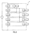
- Fig.2 illustrates in a synoptic form the diagram of Fig.1 device, the numerical references of Fig.2 corresponding to those of Fig.1.
- Fig.3 illustrates a simple realization of a source regulated current 1.
- This source includes a source of tension continues 22, for example the battery of the vehicle, delivering a voltage of 12 V.
- a voltage booster converter continue / continue 23 has its input terminals connected to those of the source 22.
- the output voltage of the converter 23 is for example 40V.
- the + output terminal of the converter 23 is connected to the anode of the LED Ln of the last floor of the series.
- the LED L0 has its cathode connected to the terminal - output of the converter 23 by via a resistor 24 in series which allows create a voltage signal for the regulation.
- a signal of command is taken by a line 25 across the 24. Line 25 provides the information to a input of a regulation incorporated in the converter 23.
- the regulation makes it possible to maintain constant intensity current flowing through the LEDs Ln ... L0. This achievement is simple.
- the transistors of the stages L1 to Ln could be of the PNP type, the base of each transistor being polarized from the lower floor, while the first stage of LED L0 would include an NPN transistor whose base would be polarized from the floor immediately superior to LED L1.
- Fig.4 shows an alternative embodiment according to which the transistor circuit of Fig.1 for an LED Ln-p is replaced by a logic circuit Bp with a MOS transistor 26 which hardly consumes current.
- the circuit Bp comprises a comparator 27, one of which non-inverting input is connected to the anode of the LED Ln-p while an inverting input is connected to a terminal 28 of an element 29 constituting a voltage reference, for example a Zener diode in which case it must include a polarization resistance.
- the other terminal of element 29 is connected to the cathode of the LED Ln-p.
- Terminal 28 is also connected to the + terminal of a floating power supply 30 whose terminal - is connected to the cathode of the LED Ln-p.
- the output of the amplifier 27 is connected to an input S a latch 31 whose output is connected to the gate of the MOS transistor 26.
- R input (reset) of the flip-flop 31 is connected to terminal 28; in fact, the R input is not used but it must be ensured that the condition of the flip-flop is R when power is turned on, which may be obtained, depending on the type of flip-flop, by the connection indicated on the diagram.
- the MOS transistor 26 has its drain connected to the anode of the LED Ln-p and its source connected to the cathode of this LED.
- the voltage across the LED Ln-p is thus applied to an input of the comparator 27, the other input is connected to voltage reference 29.
- the comparator 27 provides a signal on its output which controls a change of state of the flip-flop 31.
- the output of this rocker controls the gate of the transistor 26 that becomes conductive and bypasses the Ln-p LED which toasted.
- Such a circuit allows a reset after replacing an LED that has blown.
- PNP transistor could be replaced by a MOS transistor p-channel while the NPN transistors 2 could be replaced by channel MOS transistors not.
- transistor 2 for LED L0 would be replaced by a MOS transistor whose gate would be connected directly at point 11, without diode 7; the drain would be connected to the anode of L0, and the source would be connected to the cathode of L0.
- Zener diode 9, diode 10 and diode 6 (fuse 5) would be preserved according to the assembly of Fig.1, the fuse being designed to short-circuit the gate and the source.
- a resistance would be connected between the gate and the source of the MOS transistor; such a resistance allows, when the LED L0 then the diode 6 grill, temporarily evacuate the current between the grid and source. This resistance has a preference value much higher than the resistance 14.
- the invention allows an optimal feeding, to constant current, with a voltage booster circuit having a good potential yield, a simple structure and inexpensive, without ballast component and not causing failures in cascade.
Landscapes
- Engineering & Computer Science (AREA)
- Mechanical Engineering (AREA)
- Circuit Arrangement For Electric Light Sources In General (AREA)
- Led Devices (AREA)
- Lighting Device Outwards From Vehicle And Optical Signal (AREA)
- Led Device Packages (AREA)
- Control Of El Displays (AREA)
Abstract
Description
- un abaisseur faible tension (de l'ordre de 4 V pour des diodes InGaN) est toujours peu efficace (fort courant dans les composants) ;
- la dispersion des tensions directes des LEDs est compensée par des résistances, ou en utilisant des courants instantanés supérieurs au courant nominal. Cette dispersion est importante pour les LEDs de puissance actuellement en production (3 à 4 V pour des LEDs InGaN).
- d'alimenter des LEDs, dans une fonction à plusieurs LEDs de puissance, notamment une fonction d'éclairage automobile, dans les conditions optimales recommandées par les fabricants (c'est-à-dire à courant nominal), à un coût raisonnable,
- d'assurer que la perte d'une des LEDs, qui grille et passe en circuit ouvert, ne provoque aucune modification du fonctionnement des autres LEDs et n'entraíne donc pas l'extinction de l'ensemble.
Claims (13)
- Dispositif d'alimentation électrique pour diodes électroluminescentes (L0...Ln) montées en série, en particulier pour fonction d'éclairage, comportant une source de courant (1) commune à toutes les diodes électroluminescentes, caractérisé en ce qu'il comporte, pour chaque LED, un moyen (2,5,9 ;15,5,9) sensible à la tension aux bornes de la LED (L0,L1, ...Ln), ce moyen étant non conducteur lorsque la LED est en état de fonctionnement, et étant propre à passer en court-circuit de manière irréversible lorsque la tension aux bornes de la LED dépasse une limite prédéterminée.
- Dispositif selon la revendication 1, caractérisé en ce que le moyen sensible (2,5,9 ;15,5,9) comprend un circuit réalisé avec un transistor (2, 15) qui est bloqué, lorsque la LED (L0,..Ln-1 ; Ln) est en état de fonctionnement, par une liaison (5) entre base (3;18) et émetteur (4;16), cette liaison étant rompue lorsque la LED n'est plus en état de fonctionnement.
- Dispositif selon la revendication 2, caractérisé en ce que la liaison est assurée par un fusible (5).
- Dispositif selon la revendication 3, caractérisé en ce que le fusible (5) est constitué par une diode de signal (6).
- Dispositif selon la revendication 4, caractérisé en ce qu'une diode (7) est prévue pour constituer une compensation et empêcher un passage de courant par la base du transistor.
- Dispositif selon l'une des revendications 3 à 5, caractérisé en ce que le fusible (5) est traversé en permanence par un courant de polarisation du transistor (2, 15) qui provient d'un branchement sur un étage supérieur ou
- Dispositif selon l'une des revendications 3 à 6, caractérisé en ce que la détection de tension aux bornes d'une LED (L0, L1, ...Ln) est assurée avec une diode Zener (9) de telle sorte que, lorsque la LED grille, la tension aux bornes de cette LED dépasse la tension de Zener et le courant qui traverse la Zener (9) a une intensité supérieure à celle admissible par le fusible (5) ce qui provoque la rupture de ce dernier.
- Dispositif selon la revendication 7, caractérisé en ce qu'une diode anti-fuite (10) est prévue pour empêcher le courant de polarisation de remonter par la diode Zener (9).
- Dispositif selon l'une des revendications 2 à 8, caractérisé en ce qu'il comporte n+1 LEDs en série, auxquelles correspondent n+1 étages (de 0 à n), le circuit à transistor de chaque étage correspondant aux LEDs 0 à n-1 comporte un transistor (2) de type NPN, et la polarisation de la base (3) par rapport à l'émetteur (4) est obtenue à partir de l'étage supérieur, et pour le dernier étage (LED Ln), un circuit est prévu avec un transistor (15) de l'autre type PNP, la tension de polarisation de ce transistor PNP étant prélevée sur l'émetteur du transistor de l'étage inférieur (LED Ln-1).
- Dispositif selon l'une des revendications 2 à 10, caractérisé en ce que les circuits à transistor sont réalisés sous une forme intégrée.
- Dispositif selon l'une des revendications précédentes, caractérisé en ce qu'il comporte un convertisseur élévateur de tension continue/continue (23) avec une commande de la tension de sortie en fonction de l'intensité qui circule dans les LEDs pour réaliser une régulation de courant, le signal de commande étant pris aux bornes d'une résistance (24) montée en série avec les LEDs.
- Dispositif lumineux pour véhicule automobile tel que projecteur d'éclairage ou feu de signalisation, comportant plusieurs diodes électroluminescentes branchées en série, caractérisé en ce qu'il comporte un dispositif d'alimentation électrique selon l'une des revendications précédentes.
- Dispositif selon la revendication 12, caractérisé en ce qu'il comporte dix diodes électroluminescentes branchées en série.
Applications Claiming Priority (2)
| Application Number | Priority Date | Filing Date | Title |
|---|---|---|---|
| FR0315114A FR2864418B1 (fr) | 2003-12-19 | 2003-12-19 | Dispositif d'alimentation electrique pour diodes electroluminescentes, et projecteur lumineux comportant un tel dispositif |
| FR0315114 | 2003-12-19 |
Publications (2)
| Publication Number | Publication Date |
|---|---|
| EP1545163A1 true EP1545163A1 (fr) | 2005-06-22 |
| EP1545163B1 EP1545163B1 (fr) | 2008-01-09 |
Family
ID=34508732
Family Applications (1)
| Application Number | Title | Priority Date | Filing Date |
|---|---|---|---|
| EP04292876A Expired - Lifetime EP1545163B1 (fr) | 2003-12-19 | 2004-12-03 | Dispositif d'alimentation électrique pour diodes électroluminescentes, et projecteur lumineux comportant un tel dispositif |
Country Status (6)
| Country | Link |
|---|---|
| EP (1) | EP1545163B1 (fr) |
| JP (1) | JP4907078B2 (fr) |
| AT (1) | ATE383732T1 (fr) |
| DE (1) | DE602004011177T2 (fr) |
| ES (1) | ES2299809T3 (fr) |
| FR (1) | FR2864418B1 (fr) |
Cited By (17)
| Publication number | Priority date | Publication date | Assignee | Title |
|---|---|---|---|---|
| DE102005008100A1 (de) * | 2005-02-22 | 2006-08-31 | Mitsubishi Denki K.K. | Redundanzschaltung für in Reihe angeschlossene Dioden |
| EP1837672A1 (fr) * | 2006-03-24 | 2007-09-26 | ICS Triplex Technology Limited | Procédé et appareil de détection de défauts |
| WO2008012711A1 (fr) | 2006-07-26 | 2008-01-31 | Philips Intellectual Property & Standards Gmbh | Dispositif pour désactiver des éléments électriques en cas de dysfonctionnement |
| US7476891B2 (en) | 2006-03-24 | 2009-01-13 | Ics Triplex Technology, Ltd. | Fault detection method and apparatus |
| WO2009013675A1 (fr) * | 2007-07-23 | 2009-01-29 | Nxp B.V. | Configuration d'interrupteur de dérivation à led auto-alimentée |
| US7504975B2 (en) | 2006-03-24 | 2009-03-17 | Ics Triplex Technology Limited | Method and apparatus for output current control |
| US7613974B2 (en) | 2006-03-24 | 2009-11-03 | Ics Triplex Technology Limited | Fault detection method and apparatus |
| US7688560B2 (en) | 2006-03-24 | 2010-03-30 | Ics Triplex Technology Limited | Overload protection method |
| RU2390105C1 (ru) * | 2009-01-20 | 2010-05-20 | Анатолий Евгеньевич Хабибулин | Цветоизлучающее устройство светофора |
| US7729098B2 (en) | 2006-03-24 | 2010-06-01 | Ics Triplex Technology Limited | Overload protection method |
| US7747405B2 (en) | 2006-03-24 | 2010-06-29 | Ics Triplex Technology Ltd. | Line frequency synchronization |
| WO2011014455A1 (fr) * | 2009-07-29 | 2011-02-03 | Vektrex Electronic Systems, Inc. | Séquenceur pour del multicolore |
| DE102009035128A1 (de) * | 2009-07-29 | 2011-02-03 | Audi Ag | Schalteinrichtung für ein Kraftfahrzeug |
| WO2012023856A1 (fr) | 2010-08-20 | 2012-02-23 | Orga Holding B.V. | Carte de circuits imprimés à plusieurs del et son utilisation dans un appareil antidéflagrant |
| US8166362B2 (en) | 2006-03-24 | 2012-04-24 | Rockwell Automation Limited | Fault detection method and apparatus for analog to digital converter circuits |
| US8791645B2 (en) | 2006-02-10 | 2014-07-29 | Honeywell International Inc. | Systems and methods for controlling light sources |
| EP2852258A4 (fr) * | 2012-05-18 | 2016-07-27 | Koito Mfg Co Ltd | Dispositif de commande de source de lumière |
Families Citing this family (10)
| Publication number | Priority date | Publication date | Assignee | Title |
|---|---|---|---|---|
| JP2007161012A (ja) * | 2005-12-12 | 2007-06-28 | Koito Mfg Co Ltd | 車両用発光装置 |
| FR2901956A1 (fr) * | 2006-06-06 | 2007-12-07 | Lyracom Sarl | Procede de gestion de diodes electroluminescentes disposees en serie et lanterne incorporant des diodes electroluminescentes en serie |
| JP4926784B2 (ja) * | 2007-03-29 | 2012-05-09 | 株式会社小糸製作所 | 発光装置 |
| DE102007027951A1 (de) * | 2007-06-18 | 2008-12-24 | Tridonicatco Schweiz Ag | Schutzschaltung für eine Leuchtdiode |
| DE102009060791A1 (de) | 2009-12-22 | 2011-06-30 | Automotive Lighting Reutlingen GmbH, 72762 | Lichtmodul für eine Beleuchtungseinrichtung eines Kraftfahrzeugs sowie Beleuchtungseinrichtung eines Kraftfahrzeugs mit einem solchen Lichtmodul |
| ES2651323T3 (es) * | 2013-05-13 | 2018-01-25 | Shindengen Electric Manufacturing Co., Ltd. | Fuente de alimentación de controlador de lámpara y procedimiento para controlar la fuente de alimentación del controlador de lámpara |
| DE102014008614B4 (de) | 2014-06-07 | 2022-03-24 | Diehl Aerospace Gmbh | LED-Beleuchtungsvorrichtung für eine Wechselspannungsversorgung in einem Flugzeug sowie Flugzeug mit der LED-Beleuchtungsvorrichtung |
| CN106322188B (zh) * | 2015-07-10 | 2018-09-21 | 矽诚科技股份有限公司 | 发光二极管灯串驱动系统 |
| JP2019129108A (ja) * | 2018-01-26 | 2019-08-01 | セイコーエプソン株式会社 | 光源装置、投写型表示装置、及び、半導体装置 |
| EP4068910A1 (fr) * | 2021-03-29 | 2022-10-05 | ZKW Group GmbH | Dispositif d'éclairage détectant un défaut de court-circuit pour un phare de véhicule automobile |
Citations (5)
| Publication number | Priority date | Publication date | Assignee | Title |
|---|---|---|---|---|
| US5459328A (en) * | 1993-05-31 | 1995-10-17 | Fujitsu Limited | Driver circuit for light emitting elements connected in series and an optical amplifying repeater using the same |
| DE19841490A1 (de) * | 1998-09-10 | 2000-03-23 | Siemens Ag | Schaltungsanordnung zum Schutz einer Serienschaltung aus mindestens zwei Leuchdioden vor dem Ausfall |
| EP1006506A1 (fr) * | 1998-12-03 | 2000-06-07 | Hewlett-Packard Company | Affichage optique pour véhicule |
| US6153980A (en) * | 1999-11-04 | 2000-11-28 | Philips Electronics North America Corporation | LED array having an active shunt arrangement |
| DE10103611A1 (de) * | 2001-01-26 | 2002-08-01 | Insta Elektro Gmbh | Schaltungsanordnung zum Betreiben von mehreren Leuchtmitteln |
Family Cites Families (4)
| Publication number | Priority date | Publication date | Assignee | Title |
|---|---|---|---|---|
| JPH1168161A (ja) * | 1997-08-15 | 1999-03-09 | Digital Electron Corp | 発光装置 |
| JP2000321033A (ja) * | 1999-05-17 | 2000-11-24 | Meidensha Corp | 水晶片の計測システム |
| JP2003017574A (ja) * | 2001-06-28 | 2003-01-17 | Sanken Electric Co Ltd | 半導体装置及びこれに用いる保護回路 |
| JP2003297588A (ja) * | 2002-04-05 | 2003-10-17 | Koha Co Ltd | 発光素子点滅装置 |
-
2003
- 2003-12-19 FR FR0315114A patent/FR2864418B1/fr not_active Expired - Fee Related
-
2004
- 2004-12-03 DE DE602004011177T patent/DE602004011177T2/de not_active Expired - Lifetime
- 2004-12-03 AT AT04292876T patent/ATE383732T1/de not_active IP Right Cessation
- 2004-12-03 ES ES04292876T patent/ES2299809T3/es not_active Expired - Lifetime
- 2004-12-03 EP EP04292876A patent/EP1545163B1/fr not_active Expired - Lifetime
- 2004-12-16 JP JP2004364015A patent/JP4907078B2/ja not_active Expired - Fee Related
Patent Citations (5)
| Publication number | Priority date | Publication date | Assignee | Title |
|---|---|---|---|---|
| US5459328A (en) * | 1993-05-31 | 1995-10-17 | Fujitsu Limited | Driver circuit for light emitting elements connected in series and an optical amplifying repeater using the same |
| DE19841490A1 (de) * | 1998-09-10 | 2000-03-23 | Siemens Ag | Schaltungsanordnung zum Schutz einer Serienschaltung aus mindestens zwei Leuchdioden vor dem Ausfall |
| EP1006506A1 (fr) * | 1998-12-03 | 2000-06-07 | Hewlett-Packard Company | Affichage optique pour véhicule |
| US6153980A (en) * | 1999-11-04 | 2000-11-28 | Philips Electronics North America Corporation | LED array having an active shunt arrangement |
| DE10103611A1 (de) * | 2001-01-26 | 2002-08-01 | Insta Elektro Gmbh | Schaltungsanordnung zum Betreiben von mehreren Leuchtmitteln |
Cited By (23)
| Publication number | Priority date | Publication date | Assignee | Title |
|---|---|---|---|---|
| DE102005008100A1 (de) * | 2005-02-22 | 2006-08-31 | Mitsubishi Denki K.K. | Redundanzschaltung für in Reihe angeschlossene Dioden |
| DE102005008100B4 (de) * | 2005-02-22 | 2007-03-08 | Mitsubishi Denki K.K. | Redundanzschaltung für in Reihe angeschlossene Dioden |
| US8937443B2 (en) | 2006-02-10 | 2015-01-20 | Honeywell International Inc. | Systems and methods for controlling light sources |
| US8791645B2 (en) | 2006-02-10 | 2014-07-29 | Honeywell International Inc. | Systems and methods for controlling light sources |
| US8166362B2 (en) | 2006-03-24 | 2012-04-24 | Rockwell Automation Limited | Fault detection method and apparatus for analog to digital converter circuits |
| US7747405B2 (en) | 2006-03-24 | 2010-06-29 | Ics Triplex Technology Ltd. | Line frequency synchronization |
| US7504975B2 (en) | 2006-03-24 | 2009-03-17 | Ics Triplex Technology Limited | Method and apparatus for output current control |
| US7613974B2 (en) | 2006-03-24 | 2009-11-03 | Ics Triplex Technology Limited | Fault detection method and apparatus |
| US7688560B2 (en) | 2006-03-24 | 2010-03-30 | Ics Triplex Technology Limited | Overload protection method |
| US7476891B2 (en) | 2006-03-24 | 2009-01-13 | Ics Triplex Technology, Ltd. | Fault detection method and apparatus |
| US7729098B2 (en) | 2006-03-24 | 2010-06-01 | Ics Triplex Technology Limited | Overload protection method |
| EP1837672A1 (fr) * | 2006-03-24 | 2007-09-26 | ICS Triplex Technology Limited | Procédé et appareil de détection de défauts |
| WO2008012711A1 (fr) | 2006-07-26 | 2008-01-31 | Philips Intellectual Property & Standards Gmbh | Dispositif pour désactiver des éléments électriques en cas de dysfonctionnement |
| CN101496448B (zh) * | 2006-07-26 | 2013-01-09 | 皇家飞利浦电子股份有限公司 | 用于在故障时停用电元件的设置和方法 |
| US8174809B2 (en) | 2006-07-26 | 2012-05-08 | Koninklijke Philips Electronics N.V. | Arrangement and method for deactivating electrical elements when malfunctioning |
| CN101779523B (zh) * | 2007-07-23 | 2012-05-30 | Nxp股份有限公司 | 自供电led旁路开关配置 |
| WO2009013675A1 (fr) * | 2007-07-23 | 2009-01-29 | Nxp B.V. | Configuration d'interrupteur de dérivation à led auto-alimentée |
| US8188679B2 (en) | 2007-07-23 | 2012-05-29 | Nxp B.V. | Self-powered LED bypass-switch configuration |
| RU2390105C1 (ru) * | 2009-01-20 | 2010-05-20 | Анатолий Евгеньевич Хабибулин | Цветоизлучающее устройство светофора |
| DE102009035128A1 (de) * | 2009-07-29 | 2011-02-03 | Audi Ag | Schalteinrichtung für ein Kraftfahrzeug |
| WO2011014455A1 (fr) * | 2009-07-29 | 2011-02-03 | Vektrex Electronic Systems, Inc. | Séquenceur pour del multicolore |
| WO2012023856A1 (fr) | 2010-08-20 | 2012-02-23 | Orga Holding B.V. | Carte de circuits imprimés à plusieurs del et son utilisation dans un appareil antidéflagrant |
| EP2852258A4 (fr) * | 2012-05-18 | 2016-07-27 | Koito Mfg Co Ltd | Dispositif de commande de source de lumière |
Also Published As
| Publication number | Publication date |
|---|---|
| DE602004011177D1 (de) | 2008-02-21 |
| JP2005183975A (ja) | 2005-07-07 |
| FR2864418A1 (fr) | 2005-06-24 |
| FR2864418B1 (fr) | 2006-09-01 |
| EP1545163B1 (fr) | 2008-01-09 |
| ES2299809T3 (es) | 2008-06-01 |
| DE602004011177T2 (de) | 2009-01-02 |
| JP4907078B2 (ja) | 2012-03-28 |
| ATE383732T1 (de) | 2008-01-15 |
Similar Documents
| Publication | Publication Date | Title |
|---|---|---|
| EP1545163B1 (fr) | Dispositif d'alimentation électrique pour diodes électroluminescentes, et projecteur lumineux comportant un tel dispositif | |
| FR2846843A1 (fr) | Circuit d'allumage d'une lampe de vehicule | |
| EP3028545B1 (fr) | Dispositif a diodes electroluminescentes | |
| FR2845050A1 (fr) | Lampe de vehicule avec circuit de detection de defaillance de diode photoemissive | |
| FR3071588A1 (fr) | Circuit d'eclairage et feu de vehicule | |
| FR2881914A1 (fr) | Bloc de commande d'eclairage destine a un appareil d'eclairage de vehicule | |
| JP2004322982A (ja) | 車両用灯具 | |
| EP0509914B1 (fr) | Circuit électrique bi-tension à signalisation de défaut perfectionnée, notamment pour véhicule automobile | |
| FR2845328A1 (fr) | Lampe de vehicule a mode de fonctionnement multiple | |
| EP3589078A1 (fr) | Dispositif de pilotage de l`alimentation electrique de sources lumineuses d'un vehicule automobile en fonction des variations de leurs temperatures | |
| FR2863815A1 (fr) | Appareil et procede d'alimentation d'une lampe d'un dispositif d'affichage a cristaux liquides | |
| FR2745459A1 (fr) | Circuit d'illumination a diodes electroluminescentes, notamment pour vehicules automobiles, feu de signalisation, et tableau de commande, l'incorporant | |
| EP1039785B1 (fr) | Système de régulation de tension pour des charges embarquées dans un véhicule automobile | |
| US8106614B2 (en) | Mirror adjustment mechanism, wing mirror unit and method | |
| WO2000037281A1 (fr) | Installation de signalisation de la deceleration d'un vehicule automobile comprenant un feu emettant un flux lumineux d'intensite constante | |
| EP3416255A1 (fr) | Alimentation électrique stabilisée en modulation de largeur d'impulsions | |
| JP5079580B2 (ja) | 点灯制御装置 | |
| FR2821306A1 (fr) | Dispositif d'alimentation pour composants electriques installes dans un vehicule automobile | |
| EP0164770B1 (fr) | Relais statique pour courant continu basse tension | |
| FR2780599A1 (fr) | Circuit electrique d'eclairage d'un dispositif indicateur de vehicule automobile comportant des moyens de commande et d'asservissement | |
| JP4191368B2 (ja) | ヒューズチェック回路 | |
| FR3043302A1 (fr) | Dispositif d'illumination pour indicateur de changement de direction de vehicule a defilement | |
| FR2664785A1 (fr) | Dispositif de surveillance de circuits electriques, destine a detecter une anomalie dans le fonctionnement d'un tel circuit et application du dit dispositif a un systeme d'eclairage et/ou de signalisation de vehicule. | |
| FR2778507A1 (fr) | Circuit de securite de batterie | |
| FR2658974A1 (fr) | Dispositif d'alimentation de lampes a incandescence branchees en serie a haut degre de fiabilite. |
Legal Events
| Date | Code | Title | Description |
|---|---|---|---|
| PUAI | Public reference made under article 153(3) epc to a published international application that has entered the european phase |
Free format text: ORIGINAL CODE: 0009012 |
|
| AK | Designated contracting states |
Kind code of ref document: A1 Designated state(s): AT BE BG CH CY CZ DE DK EE ES FI FR GB GR HU IE IS IT LI LT LU MC NL PL PT RO SE SI SK TR |
|
| AX | Request for extension of the european patent |
Extension state: AL BA HR LV MK YU |
|
| 17P | Request for examination filed |
Effective date: 20051121 |
|
| AKX | Designation fees paid |
Designated state(s): AT BE BG CH CY CZ DE DK EE ES FI FR GB GR HU IE IS IT LI LT LU MC NL PL PT RO SE SI SK TR |
|
| GRAP | Despatch of communication of intention to grant a patent |
Free format text: ORIGINAL CODE: EPIDOSNIGR1 |
|
| GRAS | Grant fee paid |
Free format text: ORIGINAL CODE: EPIDOSNIGR3 |
|
| GRAA | (expected) grant |
Free format text: ORIGINAL CODE: 0009210 |
|
| AK | Designated contracting states |
Kind code of ref document: B1 Designated state(s): AT BE BG CH CY CZ DE DK EE ES FI FR GB GR HU IE IS IT LI LT LU MC NL PL PT RO SE SI SK TR |
|
| REG | Reference to a national code |
Ref country code: GB Ref legal event code: FG4D Free format text: NOT ENGLISH |
|
| REG | Reference to a national code |
Ref country code: CH Ref legal event code: EP |
|
| REG | Reference to a national code |
Ref country code: IE Ref legal event code: FG4D Free format text: LANGUAGE OF EP DOCUMENT: FRENCH |
|
| REF | Corresponds to: |
Ref document number: 602004011177 Country of ref document: DE Date of ref document: 20080221 Kind code of ref document: P |
|
| PG25 | Lapsed in a contracting state [announced via postgrant information from national office to epo] |
Ref country code: NL Free format text: LAPSE BECAUSE OF FAILURE TO SUBMIT A TRANSLATION OF THE DESCRIPTION OR TO PAY THE FEE WITHIN THE PRESCRIBED TIME-LIMIT Effective date: 20080109 Ref country code: SI Free format text: LAPSE BECAUSE OF FAILURE TO SUBMIT A TRANSLATION OF THE DESCRIPTION OR TO PAY THE FEE WITHIN THE PRESCRIBED TIME-LIMIT Effective date: 20080109 |
|
| REG | Reference to a national code |
Ref country code: ES Ref legal event code: FG2A Ref document number: 2299809 Country of ref document: ES Kind code of ref document: T3 |
|
| NLV1 | Nl: lapsed or annulled due to failure to fulfill the requirements of art. 29p and 29m of the patents act | ||
| PG25 | Lapsed in a contracting state [announced via postgrant information from national office to epo] |
Ref country code: IS Free format text: LAPSE BECAUSE OF FAILURE TO SUBMIT A TRANSLATION OF THE DESCRIPTION OR TO PAY THE FEE WITHIN THE PRESCRIBED TIME-LIMIT Effective date: 20080509 Ref country code: LT Free format text: LAPSE BECAUSE OF FAILURE TO SUBMIT A TRANSLATION OF THE DESCRIPTION OR TO PAY THE FEE WITHIN THE PRESCRIBED TIME-LIMIT Effective date: 20080109 Ref country code: FI Free format text: LAPSE BECAUSE OF FAILURE TO SUBMIT A TRANSLATION OF THE DESCRIPTION OR TO PAY THE FEE WITHIN THE PRESCRIBED TIME-LIMIT Effective date: 20080109 |
|
| GBV | Gb: ep patent (uk) treated as always having been void in accordance with gb section 77(7)/1977 [no translation filed] | ||
| PG25 | Lapsed in a contracting state [announced via postgrant information from national office to epo] |
Ref country code: BG Free format text: LAPSE BECAUSE OF FAILURE TO SUBMIT A TRANSLATION OF THE DESCRIPTION OR TO PAY THE FEE WITHIN THE PRESCRIBED TIME-LIMIT Effective date: 20080409 Ref country code: AT Free format text: LAPSE BECAUSE OF FAILURE TO SUBMIT A TRANSLATION OF THE DESCRIPTION OR TO PAY THE FEE WITHIN THE PRESCRIBED TIME-LIMIT Effective date: 20080109 |
|
| PG25 | Lapsed in a contracting state [announced via postgrant information from national office to epo] |
Ref country code: PL Free format text: LAPSE BECAUSE OF FAILURE TO SUBMIT A TRANSLATION OF THE DESCRIPTION OR TO PAY THE FEE WITHIN THE PRESCRIBED TIME-LIMIT Effective date: 20080109 Ref country code: PT Free format text: LAPSE BECAUSE OF FAILURE TO SUBMIT A TRANSLATION OF THE DESCRIPTION OR TO PAY THE FEE WITHIN THE PRESCRIBED TIME-LIMIT Effective date: 20080609 |
|
| REG | Reference to a national code |
Ref country code: IE Ref legal event code: FD4D |
|
| PG25 | Lapsed in a contracting state [announced via postgrant information from national office to epo] |
Ref country code: CZ Free format text: LAPSE BECAUSE OF FAILURE TO SUBMIT A TRANSLATION OF THE DESCRIPTION OR TO PAY THE FEE WITHIN THE PRESCRIBED TIME-LIMIT Effective date: 20080109 Ref country code: SK Free format text: LAPSE BECAUSE OF FAILURE TO SUBMIT A TRANSLATION OF THE DESCRIPTION OR TO PAY THE FEE WITHIN THE PRESCRIBED TIME-LIMIT Effective date: 20080109 Ref country code: DK Free format text: LAPSE BECAUSE OF FAILURE TO SUBMIT A TRANSLATION OF THE DESCRIPTION OR TO PAY THE FEE WITHIN THE PRESCRIBED TIME-LIMIT Effective date: 20080109 Ref country code: SE Free format text: LAPSE BECAUSE OF FAILURE TO SUBMIT A TRANSLATION OF THE DESCRIPTION OR TO PAY THE FEE WITHIN THE PRESCRIBED TIME-LIMIT Effective date: 20080409 Ref country code: IE Free format text: LAPSE BECAUSE OF FAILURE TO SUBMIT A TRANSLATION OF THE DESCRIPTION OR TO PAY THE FEE WITHIN THE PRESCRIBED TIME-LIMIT Effective date: 20080109 |
|
| PLBE | No opposition filed within time limit |
Free format text: ORIGINAL CODE: 0009261 |
|
| STAA | Information on the status of an ep patent application or granted ep patent |
Free format text: STATUS: NO OPPOSITION FILED WITHIN TIME LIMIT |
|
| PG25 | Lapsed in a contracting state [announced via postgrant information from national office to epo] |
Ref country code: RO Free format text: LAPSE BECAUSE OF FAILURE TO SUBMIT A TRANSLATION OF THE DESCRIPTION OR TO PAY THE FEE WITHIN THE PRESCRIBED TIME-LIMIT Effective date: 20080109 |
|
| 26N | No opposition filed |
Effective date: 20081010 |
|
| PG25 | Lapsed in a contracting state [announced via postgrant information from national office to epo] |
Ref country code: GB Free format text: LAPSE BECAUSE OF FAILURE TO SUBMIT A TRANSLATION OF THE DESCRIPTION OR TO PAY THE FEE WITHIN THE PRESCRIBED TIME-LIMIT Effective date: 20080109 |
|
| PG25 | Lapsed in a contracting state [announced via postgrant information from national office to epo] |
Ref country code: EE Free format text: LAPSE BECAUSE OF FAILURE TO SUBMIT A TRANSLATION OF THE DESCRIPTION OR TO PAY THE FEE WITHIN THE PRESCRIBED TIME-LIMIT Effective date: 20080109 |
|
| BERE | Be: lapsed |
Owner name: VALEO VISION Effective date: 20081231 |
|
| PG25 | Lapsed in a contracting state [announced via postgrant information from national office to epo] |
Ref country code: MC Free format text: LAPSE BECAUSE OF NON-PAYMENT OF DUE FEES Effective date: 20081231 Ref country code: CY Free format text: LAPSE BECAUSE OF FAILURE TO SUBMIT A TRANSLATION OF THE DESCRIPTION OR TO PAY THE FEE WITHIN THE PRESCRIBED TIME-LIMIT Effective date: 20080109 |
|
| REG | Reference to a national code |
Ref country code: CH Ref legal event code: PL |
|
| PG25 | Lapsed in a contracting state [announced via postgrant information from national office to epo] |
Ref country code: BE Free format text: LAPSE BECAUSE OF NON-PAYMENT OF DUE FEES Effective date: 20081231 |
|
| PG25 | Lapsed in a contracting state [announced via postgrant information from national office to epo] |
Ref country code: CH Free format text: LAPSE BECAUSE OF NON-PAYMENT OF DUE FEES Effective date: 20081231 Ref country code: LI Free format text: LAPSE BECAUSE OF NON-PAYMENT OF DUE FEES Effective date: 20081231 |
|
| PG25 | Lapsed in a contracting state [announced via postgrant information from national office to epo] |
Ref country code: LU Free format text: LAPSE BECAUSE OF NON-PAYMENT OF DUE FEES Effective date: 20081203 Ref country code: HU Free format text: LAPSE BECAUSE OF FAILURE TO SUBMIT A TRANSLATION OF THE DESCRIPTION OR TO PAY THE FEE WITHIN THE PRESCRIBED TIME-LIMIT Effective date: 20080710 |
|
| PG25 | Lapsed in a contracting state [announced via postgrant information from national office to epo] |
Ref country code: TR Free format text: LAPSE BECAUSE OF FAILURE TO SUBMIT A TRANSLATION OF THE DESCRIPTION OR TO PAY THE FEE WITHIN THE PRESCRIBED TIME-LIMIT Effective date: 20080109 |
|
| PG25 | Lapsed in a contracting state [announced via postgrant information from national office to epo] |
Ref country code: GR Free format text: LAPSE BECAUSE OF FAILURE TO SUBMIT A TRANSLATION OF THE DESCRIPTION OR TO PAY THE FEE WITHIN THE PRESCRIBED TIME-LIMIT Effective date: 20080410 |
|
| REG | Reference to a national code |
Ref country code: FR Ref legal event code: PLFP Year of fee payment: 12 |
|
| REG | Reference to a national code |
Ref country code: FR Ref legal event code: PLFP Year of fee payment: 13 |
|
| REG | Reference to a national code |
Ref country code: FR Ref legal event code: PLFP Year of fee payment: 14 |
|
| REG | Reference to a national code |
Ref country code: DE Ref legal event code: R079 Ref document number: 602004011177 Country of ref document: DE Free format text: PREVIOUS MAIN CLASS: H05B0033080000 Ipc: H05B0045000000 |
|
| PGFP | Annual fee paid to national office [announced via postgrant information from national office to epo] |
Ref country code: DE Payment date: 20191216 Year of fee payment: 16 |
|
| PGFP | Annual fee paid to national office [announced via postgrant information from national office to epo] |
Ref country code: IT Payment date: 20191216 Year of fee payment: 16 Ref country code: FR Payment date: 20191231 Year of fee payment: 16 |
|
| PGFP | Annual fee paid to national office [announced via postgrant information from national office to epo] |
Ref country code: ES Payment date: 20200124 Year of fee payment: 16 |
|
| REG | Reference to a national code |
Ref country code: DE Ref legal event code: R119 Ref document number: 602004011177 Country of ref document: DE |
|
| PG25 | Lapsed in a contracting state [announced via postgrant information from national office to epo] |
Ref country code: IT Free format text: LAPSE BECAUSE OF NON-PAYMENT OF DUE FEES Effective date: 20201203 Ref country code: FR Free format text: LAPSE BECAUSE OF NON-PAYMENT OF DUE FEES Effective date: 20201231 |
|
| PG25 | Lapsed in a contracting state [announced via postgrant information from national office to epo] |
Ref country code: DE Free format text: LAPSE BECAUSE OF NON-PAYMENT OF DUE FEES Effective date: 20210701 |
|
| REG | Reference to a national code |
Ref country code: ES Ref legal event code: FD2A Effective date: 20220207 |
|
| PG25 | Lapsed in a contracting state [announced via postgrant information from national office to epo] |
Ref country code: ES Free format text: LAPSE BECAUSE OF NON-PAYMENT OF DUE FEES Effective date: 20201204 |