EP1543537B1 - Plasma apparatus with device for reducing polymer deposition on a substrate and method for reducing polymer deposition - Google Patents
Plasma apparatus with device for reducing polymer deposition on a substrate and method for reducing polymer deposition Download PDFInfo
- Publication number
- EP1543537B1 EP1543537B1 EP03797871A EP03797871A EP1543537B1 EP 1543537 B1 EP1543537 B1 EP 1543537B1 EP 03797871 A EP03797871 A EP 03797871A EP 03797871 A EP03797871 A EP 03797871A EP 1543537 B1 EP1543537 B1 EP 1543537B1
- Authority
- EP
- European Patent Office
- Prior art keywords
- ring
- substrate
- hot edge
- coupling
- gap
- Prior art date
- Legal status (The legal status is an assumption and is not a legal conclusion. Google has not performed a legal analysis and makes no representation as to the accuracy of the status listed.)
- Expired - Lifetime
Links
- 239000000758 substrate Substances 0.000 title claims abstract description 90
- 229920000642 polymer Polymers 0.000 title claims abstract description 16
- 238000000034 method Methods 0.000 title claims description 15
- 230000008021 deposition Effects 0.000 title claims description 9
- 230000008878 coupling Effects 0.000 claims abstract description 50
- 238000010168 coupling process Methods 0.000 claims abstract description 50
- 238000005859 coupling reaction Methods 0.000 claims abstract description 50
- 230000008569 process Effects 0.000 claims description 9
- 230000009467 reduction Effects 0.000 abstract description 2
- 235000012431 wafers Nutrition 0.000 description 13
- 239000007789 gas Substances 0.000 description 10
- 238000000151 deposition Methods 0.000 description 7
- VYPSYNLAJGMNEJ-UHFFFAOYSA-N Silicium dioxide Chemical compound O=[Si]=O VYPSYNLAJGMNEJ-UHFFFAOYSA-N 0.000 description 6
- XUIMIQQOPSSXEZ-UHFFFAOYSA-N Silicon Chemical compound [Si] XUIMIQQOPSSXEZ-UHFFFAOYSA-N 0.000 description 6
- QVGXLLKOCUKJST-UHFFFAOYSA-N atomic oxygen Chemical compound [O] QVGXLLKOCUKJST-UHFFFAOYSA-N 0.000 description 6
- 239000001301 oxygen Substances 0.000 description 6
- 229910052760 oxygen Inorganic materials 0.000 description 6
- 229910052710 silicon Inorganic materials 0.000 description 6
- 239000010703 silicon Substances 0.000 description 6
- 238000004140 cleaning Methods 0.000 description 4
- 238000005530 etching Methods 0.000 description 4
- 239000000463 material Substances 0.000 description 4
- 239000010453 quartz Substances 0.000 description 4
- 239000000356 contaminant Substances 0.000 description 3
- 230000007246 mechanism Effects 0.000 description 3
- 239000003989 dielectric material Substances 0.000 description 2
- 238000009826 distribution Methods 0.000 description 2
- 239000001307 helium Substances 0.000 description 2
- 229910052734 helium Inorganic materials 0.000 description 2
- SWQJXJOGLNCZEY-UHFFFAOYSA-N helium atom Chemical compound [He] SWQJXJOGLNCZEY-UHFFFAOYSA-N 0.000 description 2
- 238000009616 inductively coupled plasma Methods 0.000 description 2
- 150000002500 ions Chemical class 0.000 description 2
- 238000005259 measurement Methods 0.000 description 2
- 239000004065 semiconductor Substances 0.000 description 2
- 229910052581 Si3N4 Inorganic materials 0.000 description 1
- ATJFFYVFTNAWJD-UHFFFAOYSA-N Tin Chemical compound [Sn] ATJFFYVFTNAWJD-UHFFFAOYSA-N 0.000 description 1
- 230000002411 adverse Effects 0.000 description 1
- PNEYBMLMFCGWSK-UHFFFAOYSA-N aluminium oxide Inorganic materials [O-2].[O-2].[O-2].[Al+3].[Al+3] PNEYBMLMFCGWSK-UHFFFAOYSA-N 0.000 description 1
- 230000015572 biosynthetic process Effects 0.000 description 1
- 239000005380 borophosphosilicate glass Substances 0.000 description 1
- 239000006227 byproduct Substances 0.000 description 1
- 239000003990 capacitor Substances 0.000 description 1
- 239000000919 ceramic Substances 0.000 description 1
- 230000008859 change Effects 0.000 description 1
- 238000006243 chemical reaction Methods 0.000 description 1
- 229910052681 coesite Inorganic materials 0.000 description 1
- 238000011109 contamination Methods 0.000 description 1
- 239000002826 coolant Substances 0.000 description 1
- 238000001816 cooling Methods 0.000 description 1
- 229910052906 cristobalite Inorganic materials 0.000 description 1
- 230000007423 decrease Effects 0.000 description 1
- 230000006866 deterioration Effects 0.000 description 1
- 230000000694 effects Effects 0.000 description 1
- 239000007772 electrode material Substances 0.000 description 1
- 238000010849 ion bombardment Methods 0.000 description 1
- 238000004519 manufacturing process Methods 0.000 description 1
- 239000005360 phosphosilicate glass Substances 0.000 description 1
- 229920002120 photoresistant polymer Polymers 0.000 description 1
- 238000005086 pumping Methods 0.000 description 1
- 229910021332 silicide Inorganic materials 0.000 description 1
- FVBUAEGBCNSCDD-UHFFFAOYSA-N silicide(4-) Chemical compound [Si-4] FVBUAEGBCNSCDD-UHFFFAOYSA-N 0.000 description 1
- 239000000377 silicon dioxide Substances 0.000 description 1
- HQVNEWCFYHHQES-UHFFFAOYSA-N silicon nitride Chemical compound N12[Si]34N5[Si]62N3[Si]51N64 HQVNEWCFYHHQES-UHFFFAOYSA-N 0.000 description 1
- 230000003068 static effect Effects 0.000 description 1
- 229910052682 stishovite Inorganic materials 0.000 description 1
- 239000000126 substance Substances 0.000 description 1
- 229910052905 tridymite Inorganic materials 0.000 description 1
Images

Classifications
-
- H—ELECTRICITY
- H01—ELECTRIC ELEMENTS
- H01L—SEMICONDUCTOR DEVICES NOT COVERED BY CLASS H10
- H01L21/00—Processes or apparatus adapted for the manufacture or treatment of semiconductor or solid state devices or of parts thereof
- H01L21/67—Apparatus specially adapted for handling semiconductor or electric solid state devices during manufacture or treatment thereof; Apparatus specially adapted for handling wafers during manufacture or treatment of semiconductor or electric solid state devices or components ; Apparatus not specifically provided for elsewhere
- H01L21/67005—Apparatus not specifically provided for elsewhere
- H01L21/67011—Apparatus for manufacture or treatment
- H01L21/67017—Apparatus for fluid treatment
- H01L21/67063—Apparatus for fluid treatment for etching
- H01L21/67069—Apparatus for fluid treatment for etching for drying etching
-
- H—ELECTRICITY
- H01—ELECTRIC ELEMENTS
- H01J—ELECTRIC DISCHARGE TUBES OR DISCHARGE LAMPS
- H01J37/00—Discharge tubes with provision for introducing objects or material to be exposed to the discharge, e.g. for the purpose of examination or processing thereof
- H01J37/32—Gas-filled discharge tubes
- H01J37/32431—Constructional details of the reactor
- H01J37/32623—Mechanical discharge control means
- H01J37/32642—Focus rings
-
- Y—GENERAL TAGGING OF NEW TECHNOLOGICAL DEVELOPMENTS; GENERAL TAGGING OF CROSS-SECTIONAL TECHNOLOGIES SPANNING OVER SEVERAL SECTIONS OF THE IPC; TECHNICAL SUBJECTS COVERED BY FORMER USPC CROSS-REFERENCE ART COLLECTIONS [XRACs] AND DIGESTS
- Y10—TECHNICAL SUBJECTS COVERED BY FORMER USPC
- Y10S—TECHNICAL SUBJECTS COVERED BY FORMER USPC CROSS-REFERENCE ART COLLECTIONS [XRACs] AND DIGESTS
- Y10S156/00—Adhesive bonding and miscellaneous chemical manufacture
- Y10S156/915—Differential etching apparatus including focus ring surrounding a wafer for plasma apparatus
Definitions
- the invention relates to an apparatus and method for reducing polymer deposition on a substrate and substrate support, and more particularly, the invention relates to the adjustment of a gap between a substrate holder and a substrate to reduce polymer deposition on exposed surfaces of the substrate holder and bottom surfaces of the substrate.
- Vacuum processing chambers are generally used for chemical vapor depositing (CVD) and etching of materials on substrates by supplying process gas to the vacuum chamber and application of an RF field to the gas.
- Examples of parallel plate, inductively coupled plasma (TCPTM, also called ICP), and electron cyclotron resonance (ECR) reactors are disclosed in commonly owned U.S. Patent Nos. 4,340,462 ; 4,948,458 ; and 5,200,232 .
- the substrates are held in place within the vacuum chamber during processing by substrate holders.
- Conventional substrate holders include mechanical clamps and electrostatic clamps (ESC). Examples of mechanical clamps and ESC substrate holders are provided in commonly owned U.S. Patent No. 5,262,029 and commonly owned U.S. Patent No. 5,671,116 .
- Substrate holders in the form of an electrode can supply radio frequency (RF) power into the chamber, as disclosed in U.S. Patent No. 4,579,618 .
- RF radio frequency
- Substrates which are etched in an oxide etching process generally include an underlayer, an oxide layer which is to be etched, and a photoresist layer formed on top of the oxide layer.
- the oxide layer may be one of SiO 2 , BPSG, PSG, or other oxide material.
- the underlayer may be Si, TiN, silicide, or other underlying layer or substrate material.
- the polymer can build up on the cooled, exposed surfaces of the chamber including exposed surfaces of a substrate support such as an electrostatic chuck and other surfaces such as a dielectric annular cap/focus ring surrounding the substrate support.
- This buildup may cause problems if it flakes off and is carried onto the top surface of the electrostatic chuck.
- These contaminants on the top surface of the chuck can prevent the chuck from operating properly to hold the wafer securely.
- the contaminants can allow helium which is supplied under the wafer as a cooling medium to leak from beneath the wafer and reduce the wafer cooling. The contaminants can also be deposited on and adversely affect the wafer itself.
- the buildup of polymer can be removed by a cleaning step performed between the processing of successive wafers.
- cleaning can be performed by injecting oxygen into the chamber, striking a plasma and reacting the oxygen with the deposited polymer to achieve an aggressive oxygen clean of the processing chamber.
- the aggressive oxygen cleaning of the processing chamber is undesirable because it adds to the wafer cycle time, reducing through-put of the system.
- the aggressive oxygen clean will shorten the lives of members within the processing chamber due to ion bombardment of these members.
- substrate processing could be carried out without a need for the aggressive oxygen cleaning step to thereby shorten cycle time and extend the life of chamber components.
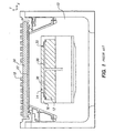
- the vacuum processing chamber 10 includes a substrate holder 12 including an electrode providing an RF bias to a substrate supported thereon.
- the substrate holder 12 includes an electrostatic clamp 14 for clamping the substrate.
- the substrate which is placed on the electrostatic clamp 14 is preferably cooled by helium backcooling (not shown) provided between the substrate and the electrostatic clamp.
- a ring 16 surrounds the electrostatic clamp 14.
- the ring 16 may be a ceramic focus ring; a combination of a focus ring, coupling ring, and edge ring; or another combination of rings.
- the vacuum processing chamber 10 includes a source of energy for maintaining a high density (e.g. 10 11 -10 12 ions/cm 3 ) plasma in the chamber such as an antenna 18 (such as a planar spiral coil or other suitable design) which is positioned above the chamber and powered by a suitable RF source.
- a suitable RF impedance matching circuit inductively couples RF into the chamber 10 so as to provide a high density plasma.
- the chamber 10 also includes a suitable vacuum pumping apparatus for maintaining the interior of the chamber at a desired pressure (e.g. below 6,6 10 -2 mbar (50 mTorr), typically 1,3 x 10 -3 mbar - 2,6 x 10 -2 mbar (1-20 mTorr).
- a dielectric window 20 (such as a uniformly thick and planar sheet of quartz, alumina, silicon nitride, etc.) is provided between the antenna 18 and the interior of the processing chamber 10 and forms the vacuum chamber wall at the top of the processing chamber 10.
- a dielectric gas distribution plate commonly called a showerhead 22, may be provided beneath the window 20 and includes a plurality of openings such as circular holes (not shown) for delivering process gas supplied by a gas supply to the processing chamber 10.
- the gas distribution plate 22 can be omitted and process gas can be supplied to the chamber by other arrangements such as gas rings, etc.
- One area in which deposits of polymer can occur in a processing chamber is a narrow gap 30 between the wafer supported on the electrostatic chuck 14 and the surrounding ring(s) 16. Specifically, a gap 30 is provided beneath the edge of the wafer which overhangs the surrounding ring. This gap 30 allows for manufacturing tolerances, thermal expansion and wear of the parts. However, process gas and volatile byproducts within the chamber 10 may migrate into the gap 30 and cause undesirable polymer deposits in the gap and on the underside edge of the wafer which may flake off and cause contamination of the wafer and/or chamber.
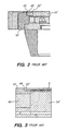
- FIG. 2 is an enlarged cross sectional view of an outer portion of an electrostatic chuck 14' and surrounded rings including a focus ring 16, a coupling ring 40, and a hot edge ring 42.
- a small vertical gap 30' is provided between an overhanging edge of the substrate S and a groove 44 provided in the edge of the hot edge ring 42.
- This vertical clearance gap 30' is designed to prevent the overhanging edge of the substrate S from being lifted and thereby avoid a reduction in clamping force applied by the electrostatic chuck 14'.
- this additional vertical clearance gap 30' provides additional opportunity for polymer buildup which may flake off and contaminate the substrate S or the electrostatic chuck 14' .
- the problem solved by the invention is to shorten the cycle time in plasma processing of substrates and to increase the life time of plasma processing chamber components.
- the plasma processing apparatus comprises a processing chamber, a power source which energizes process gas in an interior of the processing chamber into a plasma state for processing a substrate, a substrate support which supports a substrate within the interior of the processing chamber, the substrate support having an upper surface, a hot edge ring surrounding the substrate support, the hot edge ring having a portion extending under a substrate when the substrate is located on the substrate support, and a coupling ring surrounding the substrate support, the coupling ring having a first ring rotatable with respect to a second ring to adjust height of the coupling ring and adjust a gap between the hot edge ring and the substrate.
- the method of reducing polymer deposition on a substrate support in a plasma processing system comprises providing an adjustment mechanism for adjusting a gap between a substrate and a hot edge ring in a plasma processing apparatus, and adjusting the gap between the substrate and the hot edge ring by rotating a first ring with respect to a second ring of the adjustment mechanism.
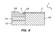
- FIG. 4 A portion of a substrate support for a vacuum processing chamber according to one embodiment of the present invention is illustrated in FIG. 4 .
- the substrate support 100 illustrated in FIG. 1 includes an electrostatic chuck 102, a focus ring 104, a coupling ring 106, and a hot edge ring 108.
- the rings surrounding the electrostatic chuck including the focus ring 104, coupling ring 106, and hot edge ring 108 help focus the ions from the RF induced plasma region on the surface of the substrate to improve process uniformity, particularly at the edge of the substrate. This is because when RF power is supplied to substrate holding chuck 102, equipotential field lines are set up over substrate and bottom electrode. These field lines are not static but change during the RF cycle. The time averaged field results in the bulk plasma being positive and the surface of the substrate and electrostatic chuck negative. Due to geometry factors, the field lines are not uniform at the edge of the substrate.
- the focus, coupling, and hot edge rings help direct the bulk of the RF coupling through substrate to the overlying plasma by acting as a capacitor between the plasma and the powered electrode (e.g., RF-powered chuck).
- the hot edge ring 108 overlays an adjustable RF coupling ring 106.
- the hot edge ring 108 is a sacrificial edge ring surrounding the electrostatic chuck 102.
- the hot edge ring 108 is a replaceable component which tends to become hot during processing of a substrate and thus is referred to as a hot edge ring.
- the hot edge ring 180 may be made from conductive electrode materials such as SiC and silicon or from dielectric materials such as quartz. By changing the edge ring material, the degree of coupling through the plasma can be tailored to provide a desired localized "edge" etch rate at the outer portion of a substrate being processed. SiC, having a lower capacitive impedance, will generally produce a faster edge etch rate than silicon. Quartz and other dielectrics will have a lesser effect on the edge etch rate.
- a gap 130 is formed between an over hanging edge of the substrate S and the silicon hot edge ring 108.
- the gap 130 has a vertical dimension d controlled by the adjustable RF coupling ring 106.
- the adjustable RF coupling ring 106 is capable of controlling the vertical dimension d of the gap by moving the silicon hot edge ring 108 in a vertical direction as appropriate. It should be noted that vertical direction is any direction substantially parallel to a Y axis, as shown in FIGS. 1 and 6 .
- the adjustable RF coupling ring 106 moveably supports the silicon hot edge ring 108.
- the adjustable RF coupling ring 106 provides mechanical support for the silicon hot edge ring 108 as well as the capability to control the gap distance d to within a specified range.
- the adjustable RF coupling ring 106 is capable of forming the gap with a 2 associated gap distance d ranging between approximately 12,7 ⁇ m (0.5 mils) to less than 152 ⁇ m (6 mils)
- the adjustable RF coupling ring 106 includes two rings 110, 112 as shown in FIG. 5 .
- the first ring 110 or top ring includes three projections 114 extending from the ring in a direction parallel to a Y axis of the ring.
- the second ring 112 or bottom ring includes three sets of a plurality of graduated steps 116 around the circumference of the ring. Rotation of the first ring 110 clockwise with respect to the second ring 112 decreases an overall vertical height of the coupling ring 106 and adjusts the gap between the substrate and the hot edge ring 108.
- the adjustable coupling ring 106 preferably includes graduated steps 116 that vary in height increments of about 2,54 ⁇ m - 254 ⁇ m (0001-0.01 inches) and preferably about 25,4 ⁇ m (0.001 inches).
- graduated steps 116 that vary in height increments of about 2,54 ⁇ m - 254 ⁇ m (0001-0.01 inches) and preferably about 25,4 ⁇ m (0.001 inches).
- the illustrated embodiment includes six graduated steps 116 in each of the three sets of steps, other numbers of steps may also be used depending on the amount of adjustment and graduation of adjustment desired.
- twelve graduated steps 116 are provided for twelve adjustment heights.
- the top ring 110 of an adjustable coupling ring 106 includes the projections 114 with a height which is equal to approximately the total height of all the steps 116 in one of the three sets of plurality of graduated steps.
- the projections 114 have a height of about 305 ⁇ m (0.012 inches).
- the adjustable coupling ring 106 can be formed of quartz.
- the adjustable RF coupling ring 106 allows the precise adjustment of the gap 130 between the substrate S and the hot edge ring 108 in a plurality of individual steps.
- the coupling ring 106 allows an operator to readjust the coupling ring at any time between processing of substrates or during set up of the vacuum processing chamber.
- the RF coupling ring 106 also ensures that the hot edge ring 108 is adjusted evenly on all sides of the substrate and that a top surface of the coupling ring remains substantially horizontal.
- the adjustable RF coupling ring 106 may be installed in new vacuum processing chambers or used to retrofit existing vacuum processing chambers to provide adjustability of the hot edge ring 108.
- a process for installing and adjusting the adjustable RF coupling ring 106 is easily implemented as follows.
- the bottom ring 112 of the coupling ring 106 is placed on the step of the electrostatic chuck 102 with the plurality of graduated steps 116 facing upward.
- the top ring 110 is then placed onto the bottom ring 112 with the three projections 114 each aligned on the highest of the graduated steps.
- the hot edge ring 108 is then placed on top of the assembled coupling ring 106 and the gap is measured with a measuring device.
- a measuring device is a vertical mount dial indicator which is placed on the substrate holding chuck 102 and measures a vertical distance from the top of the chuck to the top of the edge of the hot edge ring 108.
- the gap 130 is measured at 90 degrees apart around the electrostatic chuck.
- the measurement is taken at a location on the hot edge ring 108 close to the electrostatic chuck 102. Due to deterioration or wear of the hot edge ring, just outside the edge of the substrate, the area of the hot edge ring 108 closest to the chuck 102 should be the highest location in the hot edge ring groove.
- the measurement will generally indicate that the hot edge ring 108 is higher than the electrostatic chuck 102 and that the hot edge ring needs to be adjusted downward.
- the hot edge ring 108 is then removed.
- the coupling ring 106 is then adjusted by rotating the top ring 110 clockwise and thus reducing the height of the coupling ring.
- the hot edge ring 18 is then replaced and the adjustment is then repeated until a minimum gap distance d is achieved.
- the rings 110 and 112 of the coupling ring 106 include a locking feature (not shown) which locks the rings in an aligned radial position.
- a locking mechanism includes an detent on the top ring 110 which interlocks with grooves on each step of the bottom coupling ring 112.
- the specific shape of the focus ring 104, the coupling ring 106, and the hot edge ring 108 may vary depending on the arrangement of chuck 102, substrate and/or others. Therefore, the exact shape of the rings surrounding the chuck in FIGS. 4-6 are shown for illustration purposes only and are not limiting in any way.
Landscapes
- Engineering & Computer Science (AREA)
- Physics & Mathematics (AREA)
- Plasma & Fusion (AREA)
- Analytical Chemistry (AREA)
- Chemical & Material Sciences (AREA)
- General Physics & Mathematics (AREA)
- Microelectronics & Electronic Packaging (AREA)
- Power Engineering (AREA)
- Computer Hardware Design (AREA)
- Manufacturing & Machinery (AREA)
- Condensed Matter Physics & Semiconductors (AREA)
- Drying Of Semiconductors (AREA)
- Chemical Vapour Deposition (AREA)
- Container, Conveyance, Adherence, Positioning, Of Wafer (AREA)
- Physical Vapour Deposition (AREA)
Abstract
Description
- The invention relates to an apparatus and method for reducing polymer deposition on a substrate and substrate support, and more particularly, the invention relates to the adjustment of a gap between a substrate holder and a substrate to reduce polymer deposition on exposed surfaces of the substrate holder and bottom surfaces of the substrate.
- Vacuum processing chambers are generally used for chemical vapor depositing (CVD) and etching of materials on substrates by supplying process gas to the vacuum chamber and application of an RF field to the gas. Examples of parallel plate, inductively coupled plasma (TCP™, also called ICP), and electron cyclotron resonance (ECR) reactors are disclosed in commonly owned
U.S. Patent Nos. 4,340,462 ;4,948,458 ; and5,200,232 . The substrates are held in place within the vacuum chamber during processing by substrate holders. Conventional substrate holders include mechanical clamps and electrostatic clamps (ESC). Examples of mechanical clamps and ESC substrate holders are provided in commonly ownedU.S. Patent No. 5,262,029 and commonly ownedU.S. Patent No. 5,671,116 . Substrate holders in the form of an electrode can supply radio frequency (RF) power into the chamber, as disclosed inU.S. Patent No. 4,579,618 . - Substrates which are etched in an oxide etching process generally include an underlayer, an oxide layer which is to be etched, and a photoresist layer formed on top of the oxide layer. The oxide layer may be one of SiO2, BPSG, PSG, or other oxide material. The underlayer may be Si, TiN, silicide, or other underlying layer or substrate material. During processing of substrates, unwanted polymer deposition on the surfaces of the chamber can occur. For instance, when the chamber heats up to above 80°C during oxide etching, a reaction can occur wherein CF3 forms CF2 and HF. The formation of CF2 leads to an increase in polymer deposition on surfaces within the chamber.
- During etching of a substrate such as a semiconductor wafer in a plasma reactor, the polymer can build up on the cooled, exposed surfaces of the chamber including exposed surfaces of a substrate support such as an electrostatic chuck and other surfaces such as a dielectric annular cap/focus ring surrounding the substrate support. This buildup may cause problems if it flakes off and is carried onto the top surface of the electrostatic chuck. These contaminants on the top surface of the chuck can prevent the chuck from operating properly to hold the wafer securely. In addition, the contaminants can allow helium which is supplied under the wafer as a cooling medium to leak from beneath the wafer and reduce the wafer cooling. The contaminants can also be deposited on and adversely affect the wafer itself.
- The buildup of polymer can be removed by a cleaning step performed between the processing of successive wafers. Generally, cleaning can be performed by injecting oxygen into the chamber, striking a plasma and reacting the oxygen with the deposited polymer to achieve an aggressive oxygen clean of the processing chamber.
- The aggressive oxygen cleaning of the processing chamber is undesirable because it adds to the wafer cycle time, reducing through-put of the system. In addition, the aggressive oxygen clean will shorten the lives of members within the processing chamber due to ion bombardment of these members. As such, it would be desirable if substrate processing could be carried out without a need for the aggressive oxygen cleaning step to thereby shorten cycle time and extend the life of chamber components.
- One example of a
vacuum processing chamber 10 is illustrated inFIG. 1 . Thevacuum processing chamber 10 includes asubstrate holder 12 including an electrode providing an RF bias to a substrate supported thereon. Thesubstrate holder 12 includes anelectrostatic clamp 14 for clamping the substrate. The substrate which is placed on theelectrostatic clamp 14 is preferably cooled by helium backcooling (not shown) provided between the substrate and the electrostatic clamp. Aring 16 surrounds theelectrostatic clamp 14. Thering 16 may be a ceramic focus ring; a combination of a focus ring, coupling ring, and edge ring; or another combination of rings. - The
vacuum processing chamber 10 includes a source of energy for maintaining a high density (e.g. 1011-1012 ions/cm3) plasma in the chamber such as an antenna 18 (such as a planar spiral coil or other suitable design) which is positioned above the chamber and powered by a suitable RF source. A suitable RF impedance matching circuit, inductively couples RF into thechamber 10 so as to provide a high density plasma. Thechamber 10 also includes a suitable vacuum pumping apparatus for maintaining the interior of the chamber at a desired pressure (e.g. below 6,6 10-2 mbar (50 mTorr), typically 1,3 x 10⁻³ mbar - 2,6 x 10⁻² mbar (1-20 mTorr). A dielectric window 20 (such as a uniformly thick and planar sheet of quartz, alumina, silicon nitride, etc.) is provided between theantenna 18 and the interior of theprocessing chamber 10 and forms the vacuum chamber wall at the top of theprocessing chamber 10. A dielectric gas distribution plate, commonly called ashowerhead 22, may be provided beneath thewindow 20 and includes a plurality of openings such as circular holes (not shown) for delivering process gas supplied by a gas supply to theprocessing chamber 10. However, thegas distribution plate 22 can be omitted and process gas can be supplied to the chamber by other arrangements such as gas rings, etc. - One area in which deposits of polymer can occur in a processing chamber is a
narrow gap 30 between the wafer supported on theelectrostatic chuck 14 and the surrounding ring(s) 16. Specifically, agap 30 is provided beneath the edge of the wafer which overhangs the surrounding ring. Thisgap 30 allows for manufacturing tolerances, thermal expansion and wear of the parts. However, process gas and volatile byproducts within thechamber 10 may migrate into thegap 30 and cause undesirable polymer deposits in the gap and on the underside edge of the wafer which may flake off and cause contamination of the wafer and/or chamber. -
FIG. 2 is an enlarged cross sectional view of an outer portion of an electrostatic chuck 14' and surrounded rings including afocus ring 16, acoupling ring 40, and ahot edge ring 42. - As shown in the enlarged view of
FIG. 3 , when a substrate S in the form of a semiconductor wafer is positioned on the electrostatic chuck 14' and held in place by a suitable electrostatic clamping force a small vertical gap 30' is provided between an overhanging edge of the substrate S and a groove 44 provided in the edge of thehot edge ring 42. This vertical clearance gap 30' is designed to prevent the overhanging edge of the substrate S from being lifted and thereby avoid a reduction in clamping force applied by the electrostatic chuck 14'. However, this additional vertical clearance gap 30' provides additional opportunity for polymer buildup which may flake off and contaminate the substrate S or the electrostatic chuck 14' . - Thus, it would be desirable to reduce the vertical gap 30' between the
hot edge ring 42 or other surrounding ring and the overhanging substrate edge. - The problem solved by the invention is to shorten the cycle time in plasma processing of substrates and to increase the life time of plasma processing chamber components.
- This problem is solved by the present invention by providing a plasma processing apparatus according to claims 1 , a coupling ring for adjusting a gap between a substrate and a hot edge ring in a plasma processing apparatus according to claim 7 and by the method of reducing polymer deposition on a substrate support in a plasma processing system according to claim 9.
- The plasma processing apparatus comprises a processing chamber, a power source which energizes process gas in an interior of the processing chamber into a plasma state for processing a substrate, a substrate support which supports a substrate within the interior of the processing chamber, the substrate support having an upper surface, a hot edge ring surrounding the substrate support, the hot edge ring having a portion extending under a substrate when the substrate is located on the substrate support, and a coupling ring surrounding the substrate support, the coupling ring having a first ring rotatable with respect to a second ring to adjust height of the coupling ring and adjust a gap between the hot edge ring and the substrate.
- The method of reducing polymer deposition on a substrate support in a plasma processing system comprises providing an adjustment mechanism for adjusting a gap between a substrate and a hot edge ring in a plasma processing apparatus, and adjusting the gap between the substrate and the hot edge ring by rotating a first ring with respect to a second ring of the adjustment mechanism.
- The invention will now be described in greater detail with reference to the preferred embodiments illustrated in the accompanying drawings, in which like elements bear like reference numerals, and wherein:
-
FIG. 1 is a cross sectional view of a vacuum processing chamber; -
FIG. 2 is an enlarged cross sectional view of a portion ofFIG. 1 showing the electrostatic chuck and surrounding rings; -
FIG. 3 is an enlarged cross sectional view of portion A ofFIG. 2 ; -
FIG. 4 is an enlarged cross sectional view of a portion of a vacuum processing chamber according to the present invention including an adjustable coupling ring; -
FIG. 5 is an exploded schematic prospective view of the adjustable coupling ring ofFIG. 4 ; and -
FIG. 6 is an enlarged cross sectional view of a portion of an electrostatic chuck and focus ring showing a gap between the focus ring and substrate. - A portion of a substrate support for a vacuum processing chamber according to one embodiment of the present invention is illustrated in
FIG. 4 . Thesubstrate support 100 illustrated inFIG. 1 includes anelectrostatic chuck 102, afocus ring 104, acoupling ring 106, and ahot edge ring 108. - As is well known to those familiar with the plasma processing art, the rings surrounding the electrostatic chuck including the
focus ring 104,coupling ring 106, andhot edge ring 108 help focus the ions from the RF induced plasma region on the surface of the substrate to improve process uniformity, particularly at the edge of the substrate. This is because when RF power is supplied tosubstrate holding chuck 102, equipotential field lines are set up over substrate and bottom electrode. These field lines are not static but change during the RF cycle. The time averaged field results in the bulk plasma being positive and the surface of the substrate and electrostatic chuck negative. Due to geometry factors, the field lines are not uniform at the edge of the substrate. The focus, coupling, and hot edge rings help direct the bulk of the RF coupling through substrate to the overlying plasma by acting as a capacitor between the plasma and the powered electrode (e.g., RF-powered chuck). - The
hot edge ring 108 overlays an adjustableRF coupling ring 106. Thehot edge ring 108 is a sacrificial edge ring surrounding theelectrostatic chuck 102. Thehot edge ring 108 is a replaceable component which tends to become hot during processing of a substrate and thus is referred to as a hot edge ring. The hot edge ring 180 may be made from conductive electrode materials such as SiC and silicon or from dielectric materials such as quartz. By changing the edge ring material, the degree of coupling through the plasma can be tailored to provide a desired localized "edge" etch rate at the outer portion of a substrate being processed. SiC, having a lower capacitive impedance, will generally produce a faster edge etch rate than silicon. Quartz and other dielectrics will have a lesser effect on the edge etch rate. - In the described embodiment a
gap 130, shown inFIG. 6 , is formed between an over hanging edge of the substrate S and the siliconhot edge ring 108. Thegap 130 has a vertical dimension d controlled by the adjustableRF coupling ring 106. The adjustableRF coupling ring 106 is capable of controlling the vertical dimension d of the gap by moving the siliconhot edge ring 108 in a vertical direction as appropriate. It should be noted that vertical direction is any direction substantially parallel to a Y axis, as shown inFIGS. 1 and6 . - In accordance with one embodiment of the invention, the adjustable
RF coupling ring 106 moveably supports the siliconhot edge ring 108. The adjustableRF coupling ring 106 provides mechanical support for the siliconhot edge ring 108 as well as the capability to control the gap distance d to within a specified range. In one aspect of the invention, the adjustableRF coupling ring 106 is capable of forming the gap with a 2 associated gap distance d ranging between approximately 12,7µm (0.5 mils) to less than 152 µm (6 mils) - In the described embodiment, the adjustable
RF coupling ring 106 includes tworings FIG. 5 . Thefirst ring 110 or top ring includes threeprojections 114 extending from the ring in a direction parallel to a Y axis of the ring. Thesecond ring 112 or bottom ring includes three sets of a plurality ofgraduated steps 116 around the circumference of the ring. Rotation of thefirst ring 110 clockwise with respect to thesecond ring 112 decreases an overall vertical height of thecoupling ring 106 and adjusts the gap between the substrate and thehot edge ring 108. - In the described embodiment, the
adjustable coupling ring 106 preferably includes graduatedsteps 116 that vary in height increments of about 2,54 µm - 254 µm (0001-0.01 inches) and preferably about 25,4 µm (0.001 inches). Although the illustrated embodiment includes six graduatedsteps 116 in each of the three sets of steps, other numbers of steps may also be used depending on the amount of adjustment and graduation of adjustment desired. According to another embodiment twelve graduatedsteps 116 are provided for twelve adjustment heights. - In the described embodiment, the
top ring 110 of anadjustable coupling ring 106 includes theprojections 114 with a height which is equal to approximately the total height of all thesteps 116 in one of the three sets of plurality of graduated steps. In a preferred embodiment, theprojections 114 have a height of about 305 µm (0.012 inches). In the described embodiment, theadjustable coupling ring 106 can be formed of quartz. - The adjustable
RF coupling ring 106 according to the present invention, allows the precise adjustment of thegap 130 between the substrate S and thehot edge ring 108 in a plurality of individual steps. Thecoupling ring 106 allows an operator to readjust the coupling ring at any time between processing of substrates or during set up of the vacuum processing chamber. TheRF coupling ring 106 also ensures that thehot edge ring 108 is adjusted evenly on all sides of the substrate and that a top surface of the coupling ring remains substantially horizontal. - The adjustable
RF coupling ring 106 may be installed in new vacuum processing chambers or used to retrofit existing vacuum processing chambers to provide adjustability of thehot edge ring 108. - A process for installing and adjusting the adjustable
RF coupling ring 106 is easily implemented as follows. Thebottom ring 112 of thecoupling ring 106 is placed on the step of theelectrostatic chuck 102 with the plurality ofgraduated steps 116 facing upward. Thetop ring 110 is then placed onto thebottom ring 112 with the threeprojections 114 each aligned on the highest of the graduated steps. Thehot edge ring 108 is then placed on top of the assembledcoupling ring 106 and the gap is measured with a measuring device. One example of a measuring device is a vertical mount dial indicator which is placed on thesubstrate holding chuck 102 and measures a vertical distance from the top of the chuck to the top of the edge of thehot edge ring 108. Preferably, thegap 130 is measured at 90 degrees apart around the electrostatic chuck. The measurement is taken at a location on thehot edge ring 108 close to theelectrostatic chuck 102. Due to deterioration or wear of the hot edge ring, just outside the edge of the substrate, the area of thehot edge ring 108 closest to thechuck 102 should be the highest location in the hot edge ring groove. The measurement will generally indicate that thehot edge ring 108 is higher than theelectrostatic chuck 102 and that the hot edge ring needs to be adjusted downward. Thehot edge ring 108 is then removed. Thecoupling ring 106 is then adjusted by rotating thetop ring 110 clockwise and thus reducing the height of the coupling ring. Thehot edge ring 18 is then replaced and the adjustment is then repeated until a minimum gap distance d is achieved. - According to one preferred embodiment of the invention, the
rings coupling ring 106 include a locking feature (not shown) which locks the rings in an aligned radial position. One example of a locking mechanism includes an detent on thetop ring 110 which interlocks with grooves on each step of thebottom coupling ring 112. - It should be appreciated that in a specific system, the specific shape of the
focus ring 104, thecoupling ring 106, and thehot edge ring 108 may vary depending on the arrangement ofchuck 102, substrate and/or others. Therefore, the exact shape of the rings surrounding the chuck inFIGS. 4-6 are shown for illustration purposes only and are not limiting in any way.
Claims (10)
- A plasma processing apparatus comprising:a processing chamber (10);a power source (18) which energizes process gas in an interior of the professing chamber (10) into a plasma state for processing a substrate;a substrate support (100) which supports a substrate within the interior of the processing chamber (10), the substrate support (100) having an upper surface;a hot edge ring (108) surrounding the substrate support (100), the hot edge ring (108) having a portion extending under a substrate when the substrate is located on the substrate support (100); anda coupling ring (106) surrounding the substrate support (100) and supporting the hot edge ring (108),characterized bythe coupling ring (106) having a first ring (110) rotatable with respect to a second ring (112) to adjust height of the coupling ring (106) and adjust a gap (130) between the hot edge ring (108) and the substrate.
- The apparatus of Claim 1, wherein the coupling ring (106) is arranged to adjust a distance between a lower surface of the substrate and an upper surface of the portion of the hot edge ring (108) extending under the substrate by rotation of the first ring (110) with respect to the second ring (112).
- The apparatus of Claim 1, wherein the second ring (112) comprises a plurality of stepped surfaces (116).
- The apparatus of Claim3, wherein the coupling ring (106) comprises:a first ring (110) having at least three projections (114) extending from the ring in a direction parallel to an axis of the ring; anda second ring (112) having at least three sets of a plurality of steps (116) arranged to receive each of the at least three projections (114), wherein a total thickness of the first and second ring (110, 112) is adjustable by rotation of the first ring (110) with respect to the second ring (112).
- The apparatus of Claim 4, wherein the steps (116) each have a height of about 25,4 µm (.001 inches).
- The apparatus of Claim 1, wherein substrate support (100) comprises an electrostatic chuck (102).
- A coupling ring (106) for adjusting a gap (130) between a substrate and a hot edge ring (108) in a plasma processing apparatus, the coupling ring (106) comprising:a first ring (110) having at least three projections (114) extending from the ring (110) in a direction parallel to an axis of the ring (110); anda second ring (112) having at least three sets of a plurality of steps (116) arranged to receive each of the at least three projections (114), wherein a total thickness of the first and second ring (110, 112) is adjustable by rotation of the first ring (110) with respect to the second ring (112).
- The coupling ring (106) of Claim 7, wherein the steps each have a height of about 25,4 µm (.001 inches).
- A method of reducing polymer deposition on a substrate support (100) in a plasma processing system comprising:providing a coupling ring (106) for supporting a hot edge ring (108) and for adjusting a gap (130) between a substrate and said hot edge ring (108) in a plasma processing apparatus;the hot edge ring (108) surrounding the substrate support (100) and having a portion extending under a substrate when the substrate is located on the substrate support (100); andcharacterized byadjusting the gap (130) between the substrate and the hot edge ring (108) by rotating a first ring (110) with respect to a second ring (112) of the coupling ring (106) wherein a total thickness of the first and second ring (110, 112) is adjustable by rotation of the first ring (110) with respect to the second ring (112).
- The method of Claim 9, wherein the coupling ring (106) is placed between a focus ring (104) and the hot edge ring (108).
Applications Claiming Priority (3)
| Application Number | Priority Date | Filing Date | Title |
|---|---|---|---|
| US10/251,179 US7252738B2 (en) | 2002-09-20 | 2002-09-20 | Apparatus for reducing polymer deposition on a substrate and substrate support |
| US251179 | 2002-09-20 | ||
| PCT/US2003/027055 WO2004027815A1 (en) | 2002-09-20 | 2003-08-28 | Plasma apparatus with device for reducing polymer deposition on a substrate and method for reducing polymer deposition |
Publications (2)
| Publication Number | Publication Date |
|---|---|
| EP1543537A1 EP1543537A1 (en) | 2005-06-22 |
| EP1543537B1 true EP1543537B1 (en) | 2011-10-05 |
Family
ID=32028995
Family Applications (1)
| Application Number | Title | Priority Date | Filing Date |
|---|---|---|---|
| EP03797871A Expired - Lifetime EP1543537B1 (en) | 2002-09-20 | 2003-08-28 | Plasma apparatus with device for reducing polymer deposition on a substrate and method for reducing polymer deposition |
Country Status (9)
| Country | Link |
|---|---|
| US (2) | US7252738B2 (en) |
| EP (1) | EP1543537B1 (en) |
| JP (1) | JP4499567B2 (en) |
| KR (1) | KR101008863B1 (en) |
| CN (2) | CN100351989C (en) |
| AT (1) | ATE527679T1 (en) |
| AU (1) | AU2003260128A1 (en) |
| TW (1) | TWI324804B (en) |
| WO (1) | WO2004027815A1 (en) |
Families Citing this family (343)
| Publication number | Priority date | Publication date | Assignee | Title |
|---|---|---|---|---|
| US7850174B2 (en) * | 2003-01-07 | 2010-12-14 | Tokyo Electron Limited | Plasma processing apparatus and focus ring |
| US20060226003A1 (en) * | 2003-01-22 | 2006-10-12 | John Mize | Apparatus and methods for ionized deposition of a film or thin layer |
| JP4472372B2 (en) * | 2003-02-03 | 2010-06-02 | 株式会社オクテック | Plasma processing apparatus and electrode plate for plasma processing apparatus |
| US20060000802A1 (en) * | 2004-06-30 | 2006-01-05 | Ajay Kumar | Method and apparatus for photomask plasma etching |
| US8349128B2 (en) | 2004-06-30 | 2013-01-08 | Applied Materials, Inc. | Method and apparatus for stable plasma processing |
| KR100610010B1 (en) * | 2004-07-20 | 2006-08-08 | 삼성전자주식회사 | Apparatus for |
| US7457097B2 (en) * | 2004-07-27 | 2008-11-25 | International Business Machines Corporation | Pressure assisted wafer holding apparatus and control method |
| GB0424371D0 (en) * | 2004-11-04 | 2004-12-08 | Trikon Technologies Ltd | Shielding design for backside metal deposition |
| US20060172542A1 (en) * | 2005-01-28 | 2006-08-03 | Applied Materials, Inc. | Method and apparatus to confine plasma and to enhance flow conductance |
| US9659758B2 (en) | 2005-03-22 | 2017-05-23 | Honeywell International Inc. | Coils utilized in vapor deposition applications and methods of production |
| US20060278520A1 (en) * | 2005-06-13 | 2006-12-14 | Lee Eal H | Use of DC magnetron sputtering systems |
| JP5043826B2 (en) * | 2006-02-23 | 2012-10-10 | 株式会社日立国際電気 | Substrate processing apparatus and semiconductor device manufacturing method |
| US20070215607A1 (en) * | 2006-03-20 | 2007-09-20 | Wander Joseph M | Apparatus and method for heating semiconductor wafers via microwares |
| US7723648B2 (en) * | 2006-09-25 | 2010-05-25 | Tokyo Electron Limited | Temperature controlled substrate holder with non-uniform insulation layer for a substrate processing system |
| US7838800B2 (en) * | 2006-09-25 | 2010-11-23 | Tokyo Electron Limited | Temperature controlled substrate holder having erosion resistant insulating layer for a substrate processing system |
| US7909961B2 (en) * | 2006-10-30 | 2011-03-22 | Applied Materials, Inc. | Method and apparatus for photomask plasma etching |
| US7943005B2 (en) | 2006-10-30 | 2011-05-17 | Applied Materials, Inc. | Method and apparatus for photomask plasma etching |
| US7837827B2 (en) * | 2007-06-28 | 2010-11-23 | Lam Research Corporation | Edge ring arrangements for substrate processing |
| US8563619B2 (en) * | 2007-06-28 | 2013-10-22 | Lam Research Corporation | Methods and arrangements for plasma processing system with tunable capacitance |
| US20090025636A1 (en) * | 2007-07-27 | 2009-01-29 | Applied Materials, Inc. | High profile minimum contact process kit for hdp-cvd application |
| KR100892928B1 (en) * | 2007-09-05 | 2009-04-09 | 주식회사 에이디피엔지니어링 | Lower eletrode assembly of manufacturing FPD |
| US20090162570A1 (en) * | 2007-12-19 | 2009-06-25 | Applied Materials, Inc. | Apparatus and method for processing a substrate using inductively coupled plasma technology |
| US8999106B2 (en) * | 2007-12-19 | 2015-04-07 | Applied Materials, Inc. | Apparatus and method for controlling edge performance in an inductively coupled plasma chamber |
| CN101488468B (en) * | 2008-01-17 | 2010-12-08 | 北京北方微电子基地设备工艺研究中心有限责任公司 | Wafer retaining system and semiconductor processing apparatus applying the system |
| US20090194414A1 (en) * | 2008-01-31 | 2009-08-06 | Nolander Ira G | Modified sputtering target and deposition components, methods of production and uses thereof |
| JP2010045200A (en) * | 2008-08-13 | 2010-02-25 | Tokyo Electron Ltd | Focus ring, and plasma processing apparatus and method |
| US8449679B2 (en) * | 2008-08-15 | 2013-05-28 | Lam Research Corporation | Temperature controlled hot edge ring assembly |
| US8454027B2 (en) * | 2008-09-26 | 2013-06-04 | Lam Research Corporation | Adjustable thermal contact between an electrostatic chuck and a hot edge ring by clocking a coupling ring |
| US20100101729A1 (en) * | 2008-10-28 | 2010-04-29 | Applied Materials, Inc. | Process kit having reduced erosion sensitivity |
| US9394608B2 (en) | 2009-04-06 | 2016-07-19 | Asm America, Inc. | Semiconductor processing reactor and components thereof |
| US8272346B2 (en) * | 2009-04-10 | 2012-09-25 | Lam Research Corporation | Gasket with positioning feature for clamped monolithic showerhead electrode |
| CN101994087B (en) * | 2009-08-14 | 2013-04-24 | 鸿富锦精密工业(深圳)有限公司 | Evaporating deposition device |
| US8802201B2 (en) | 2009-08-14 | 2014-08-12 | Asm America, Inc. | Systems and methods for thin-film deposition of metal oxides using excited nitrogen-oxygen species |
| TWI385725B (en) * | 2009-09-18 | 2013-02-11 | Advanced Micro Fab Equip Inc | A structure that reduces the deposition of polymer on the backside of the substrate |
| SG170717A1 (en) * | 2009-11-02 | 2011-05-30 | Lam Res Corp | Hot edge ring with sloped upper surface |
| DE202010015933U1 (en) * | 2009-12-01 | 2011-03-31 | Lam Research Corp.(N.D.Ges.D.Staates Delaware), Fremont | An edge ring arrangement for plasma etching chambers |
| US9111729B2 (en) * | 2009-12-03 | 2015-08-18 | Lam Research Corporation | Small plasma chamber systems and methods |
| US9190289B2 (en) * | 2010-02-26 | 2015-11-17 | Lam Research Corporation | System, method and apparatus for plasma etch having independent control of ion generation and dissociation of process gas |
| US9967965B2 (en) | 2010-08-06 | 2018-05-08 | Lam Research Corporation | Distributed, concentric multi-zone plasma source systems, methods and apparatus |
| US8999104B2 (en) | 2010-08-06 | 2015-04-07 | Lam Research Corporation | Systems, methods and apparatus for separate plasma source control |
| US9155181B2 (en) | 2010-08-06 | 2015-10-06 | Lam Research Corporation | Distributed multi-zone plasma source systems, methods and apparatus |
| US9449793B2 (en) | 2010-08-06 | 2016-09-20 | Lam Research Corporation | Systems, methods and apparatus for choked flow element extraction |
| US9129795B2 (en) | 2011-04-11 | 2015-09-08 | Quadrant Epp Ag | Process for plasma treatment employing ceramic-filled polyamideimide composite parts |
| EP2525387A1 (en) | 2011-05-17 | 2012-11-21 | Quadrant Epp Ag | Process for plasma treatment employing ceramic-filled polyamideimide composite parts |
| US9312155B2 (en) | 2011-06-06 | 2016-04-12 | Asm Japan K.K. | High-throughput semiconductor-processing apparatus equipped with multiple dual-chamber modules |
| US10854498B2 (en) | 2011-07-15 | 2020-12-01 | Asm Ip Holding B.V. | Wafer-supporting device and method for producing same |
| US20130023129A1 (en) | 2011-07-20 | 2013-01-24 | Asm America, Inc. | Pressure transmitter for a semiconductor processing environment |
| US9017481B1 (en) | 2011-10-28 | 2015-04-28 | Asm America, Inc. | Process feed management for semiconductor substrate processing |
| US9177762B2 (en) | 2011-11-16 | 2015-11-03 | Lam Research Corporation | System, method and apparatus of a wedge-shaped parallel plate plasma reactor for substrate processing |
| US10283325B2 (en) | 2012-10-10 | 2019-05-07 | Lam Research Corporation | Distributed multi-zone plasma source systems, methods and apparatus |
| US9508530B2 (en) | 2011-11-21 | 2016-11-29 | Lam Research Corporation | Plasma processing chamber with flexible symmetric RF return strap |
| US8872525B2 (en) * | 2011-11-21 | 2014-10-28 | Lam Research Corporation | System, method and apparatus for detecting DC bias in a plasma processing chamber |
| US9083182B2 (en) | 2011-11-21 | 2015-07-14 | Lam Research Corporation | Bypass capacitors for high voltage bias power in the mid frequency RF range |
| US8898889B2 (en) | 2011-11-22 | 2014-12-02 | Lam Research Corporation | Chuck assembly for plasma processing |
| US9396908B2 (en) | 2011-11-22 | 2016-07-19 | Lam Research Corporation | Systems and methods for controlling a plasma edge region |
| US10586686B2 (en) | 2011-11-22 | 2020-03-10 | Law Research Corporation | Peripheral RF feed and symmetric RF return for symmetric RF delivery |
| US9263240B2 (en) | 2011-11-22 | 2016-02-16 | Lam Research Corporation | Dual zone temperature control of upper electrodes |
| US8677586B2 (en) * | 2012-04-04 | 2014-03-25 | Lam Research Corporation | Installation fixture for elastomer bands and methods of using the same |
| US9184030B2 (en) | 2012-07-19 | 2015-11-10 | Lam Research Corporation | Edge exclusion control with adjustable plasma exclusion zone ring |
| CN103074610A (en) * | 2012-08-28 | 2013-05-01 | 光达光电设备科技(嘉兴)有限公司 | Substrate supporting structure and reaction chamber containing the same |
| US9048190B2 (en) * | 2012-10-09 | 2015-06-02 | Applied Materials, Inc. | Methods and apparatus for processing substrates using an ion shield |
| US10714315B2 (en) | 2012-10-12 | 2020-07-14 | Asm Ip Holdings B.V. | Semiconductor reaction chamber showerhead |
| JP2014107387A (en) | 2012-11-27 | 2014-06-09 | Tokyo Electron Ltd | Pedestal structure and method of holding focus ring |
| CN103117239B (en) * | 2013-02-01 | 2017-02-01 | 上海华虹宏力半导体制造有限公司 | Navigating piece used for dry etching equipment and navigating method |
| US20160376700A1 (en) | 2013-02-01 | 2016-12-29 | Asm Ip Holding B.V. | System for treatment of deposition reactor |
| US9502279B2 (en) | 2013-06-28 | 2016-11-22 | Lam Research Corporation | Installation fixture having a micro-grooved non-stick surface |
| CN105453234B (en) * | 2013-08-10 | 2018-11-02 | 应用材料公司 | The method for polishing new or renovation electrostatic chuck |
| CN104726830B (en) * | 2013-12-24 | 2017-06-30 | 宁波江丰电子材料股份有限公司 | The correcting device of focusing ring |
| CN104752141B (en) * | 2013-12-31 | 2017-02-08 | 中微半导体设备(上海)有限公司 | Plasma processing device and operating method thereof |
| US10683571B2 (en) | 2014-02-25 | 2020-06-16 | Asm Ip Holding B.V. | Gas supply manifold and method of supplying gases to chamber using same |
| US10167557B2 (en) | 2014-03-18 | 2019-01-01 | Asm Ip Holding B.V. | Gas distribution system, reactor including the system, and methods of using the same |
| US11015245B2 (en) | 2014-03-19 | 2021-05-25 | Asm Ip Holding B.V. | Gas-phase reactor and system having exhaust plenum and components thereof |
| US10858737B2 (en) | 2014-07-28 | 2020-12-08 | Asm Ip Holding B.V. | Showerhead assembly and components thereof |
| US9890456B2 (en) | 2014-08-21 | 2018-02-13 | Asm Ip Holding B.V. | Method and system for in situ formation of gas-phase compounds |
| US10941490B2 (en) | 2014-10-07 | 2021-03-09 | Asm Ip Holding B.V. | Multiple temperature range susceptor, assembly, reactor and system including the susceptor, and methods of using the same |
| US9657845B2 (en) | 2014-10-07 | 2017-05-23 | Asm Ip Holding B.V. | Variable conductance gas distribution apparatus and method |
| JP2016134572A (en) * | 2015-01-21 | 2016-07-25 | ルネサスエレクトロニクス株式会社 | Semiconductor manufacturing apparatus and management method of the same, and semiconductor device manufacturing method |
| US10276355B2 (en) | 2015-03-12 | 2019-04-30 | Asm Ip Holding B.V. | Multi-zone reactor, system including the reactor, and method of using the same |
| US10903055B2 (en) * | 2015-04-17 | 2021-01-26 | Applied Materials, Inc. | Edge ring for bevel polymer reduction |
| JP1551512S (en) * | 2015-06-12 | 2016-06-13 | ||
| US10458018B2 (en) | 2015-06-26 | 2019-10-29 | Asm Ip Holding B.V. | Structures including metal carbide material, devices including the structures, and methods of forming same |
| US10600673B2 (en) | 2015-07-07 | 2020-03-24 | Asm Ip Holding B.V. | Magnetic susceptor to baseplate seal |
| KR20170014384A (en) * | 2015-07-30 | 2017-02-08 | 삼성전자주식회사 | Dry etching apparatus |
| US10211308B2 (en) | 2015-10-21 | 2019-02-19 | Asm Ip Holding B.V. | NbMC layers |
| US11139308B2 (en) | 2015-12-29 | 2021-10-05 | Asm Ip Holding B.V. | Atomic layer deposition of III-V compounds to form V-NAND devices |
| KR20180099776A (en) | 2016-01-26 | 2018-09-05 | 어플라이드 머티어리얼스, 인코포레이티드 | Wafer edge ring lifting solution |
| KR101646716B1 (en) * | 2016-02-15 | 2016-08-08 | 서성환 | spacer and assembly spiral stairway in use with the spacer |
| US10529554B2 (en) | 2016-02-19 | 2020-01-07 | Asm Ip Holding B.V. | Method for forming silicon nitride film selectively on sidewalls or flat surfaces of trenches |
| US10865475B2 (en) | 2016-04-21 | 2020-12-15 | Asm Ip Holding B.V. | Deposition of metal borides and silicides |
| US10190213B2 (en) | 2016-04-21 | 2019-01-29 | Asm Ip Holding B.V. | Deposition of metal borides |
| US10032628B2 (en) | 2016-05-02 | 2018-07-24 | Asm Ip Holding B.V. | Source/drain performance through conformal solid state doping |
| US10367080B2 (en) | 2016-05-02 | 2019-07-30 | Asm Ip Holding B.V. | Method of forming a germanium oxynitride film |
| US11453943B2 (en) | 2016-05-25 | 2022-09-27 | Asm Ip Holding B.V. | Method for forming carbon-containing silicon/metal oxide or nitride film by ALD using silicon precursor and hydrocarbon precursor |
| US9852889B1 (en) | 2016-06-22 | 2017-12-26 | Lam Research Corporation | Systems and methods for controlling directionality of ions in an edge region by using an electrode within a coupling ring |
| JP6700118B2 (en) * | 2016-06-24 | 2020-05-27 | 東京エレクトロン株式会社 | Plasma deposition apparatus and substrate mounting table |
| US10612137B2 (en) | 2016-07-08 | 2020-04-07 | Asm Ip Holdings B.V. | Organic reactants for atomic layer deposition |
| US9859151B1 (en) | 2016-07-08 | 2018-01-02 | Asm Ip Holding B.V. | Selective film deposition method to form air gaps |
| US10714385B2 (en) | 2016-07-19 | 2020-07-14 | Asm Ip Holding B.V. | Selective deposition of tungsten |
| US9887082B1 (en) | 2016-07-28 | 2018-02-06 | Asm Ip Holding B.V. | Method and apparatus for filling a gap |
| KR102532607B1 (en) | 2016-07-28 | 2023-05-15 | 에이에스엠 아이피 홀딩 비.브이. | Substrate processing apparatus and method of operating the same |
| US9812320B1 (en) | 2016-07-28 | 2017-11-07 | Asm Ip Holding B.V. | Method and apparatus for filling a gap |
| US10643826B2 (en) | 2016-10-26 | 2020-05-05 | Asm Ip Holdings B.V. | Methods for thermally calibrating reaction chambers |
| US11532757B2 (en) | 2016-10-27 | 2022-12-20 | Asm Ip Holding B.V. | Deposition of charge trapping layers |
| US10622243B2 (en) * | 2016-10-28 | 2020-04-14 | Lam Research Corporation | Planar substrate edge contact with open volume equalization pathways and side containment |
| US10643904B2 (en) | 2016-11-01 | 2020-05-05 | Asm Ip Holdings B.V. | Methods for forming a semiconductor device and related semiconductor device structures |
| US10714350B2 (en) | 2016-11-01 | 2020-07-14 | ASM IP Holdings, B.V. | Methods for forming a transition metal niobium nitride film on a substrate by atomic layer deposition and related semiconductor device structures |
| US10229833B2 (en) | 2016-11-01 | 2019-03-12 | Asm Ip Holding B.V. | Methods for forming a transition metal nitride film on a substrate by atomic layer deposition and related semiconductor device structures |
| US10134757B2 (en) | 2016-11-07 | 2018-11-20 | Asm Ip Holding B.V. | Method of processing a substrate and a device manufactured by using the method |
| KR102546317B1 (en) | 2016-11-15 | 2023-06-21 | 에이에스엠 아이피 홀딩 비.브이. | Gas supply unit and substrate processing apparatus including the same |
| KR20180068582A (en) | 2016-12-14 | 2018-06-22 | 에이에스엠 아이피 홀딩 비.브이. | Substrate processing apparatus |
| US11581186B2 (en) | 2016-12-15 | 2023-02-14 | Asm Ip Holding B.V. | Sequential infiltration synthesis apparatus |
| US11447861B2 (en) | 2016-12-15 | 2022-09-20 | Asm Ip Holding B.V. | Sequential infiltration synthesis apparatus and a method of forming a patterned structure |
| US11251019B2 (en) * | 2016-12-15 | 2022-02-15 | Toyota Jidosha Kabushiki Kaisha | Plasma device |
| US9947517B1 (en) * | 2016-12-16 | 2018-04-17 | Applied Materials, Inc. | Adjustable extended electrode for edge uniformity control |
| KR20180070971A (en) | 2016-12-19 | 2018-06-27 | 에이에스엠 아이피 홀딩 비.브이. | Substrate processing apparatus |
| US10269558B2 (en) | 2016-12-22 | 2019-04-23 | Asm Ip Holding B.V. | Method of forming a structure on a substrate |
| US10867788B2 (en) | 2016-12-28 | 2020-12-15 | Asm Ip Holding B.V. | Method of forming a structure on a substrate |
| US11390950B2 (en) | 2017-01-10 | 2022-07-19 | Asm Ip Holding B.V. | Reactor system and method to reduce residue buildup during a film deposition process |
| US10553404B2 (en) | 2017-02-01 | 2020-02-04 | Applied Materials, Inc. | Adjustable extended electrode for edge uniformity control |
| US10655221B2 (en) | 2017-02-09 | 2020-05-19 | Asm Ip Holding B.V. | Method for depositing oxide film by thermal ALD and PEALD |
| US10468261B2 (en) | 2017-02-15 | 2019-11-05 | Asm Ip Holding B.V. | Methods for forming a metallic film on a substrate by cyclical deposition and related semiconductor device structures |
| US10529563B2 (en) | 2017-03-29 | 2020-01-07 | Asm Ip Holdings B.V. | Method for forming doped metal oxide films on a substrate by cyclical deposition and related semiconductor device structures |
| US11195704B2 (en) | 2017-03-31 | 2021-12-07 | Beijing E-town Semiconductor Technology Co., Ltd. | Pedestal assembly for plasma processing apparatus |
| USD876504S1 (en) | 2017-04-03 | 2020-02-25 | Asm Ip Holding B.V. | Exhaust flow control ring for semiconductor deposition apparatus |
| KR102457289B1 (en) | 2017-04-25 | 2022-10-21 | 에이에스엠 아이피 홀딩 비.브이. | Method for depositing a thin film and manufacturing a semiconductor device |
| US10892156B2 (en) | 2017-05-08 | 2021-01-12 | Asm Ip Holding B.V. | Methods for forming a silicon nitride film on a substrate and related semiconductor device structures |
| US10770286B2 (en) | 2017-05-08 | 2020-09-08 | Asm Ip Holdings B.V. | Methods for selectively forming a silicon nitride film on a substrate and related semiconductor device structures |
| US11306395B2 (en) | 2017-06-28 | 2022-04-19 | Asm Ip Holding B.V. | Methods for depositing a transition metal nitride film on a substrate by atomic layer deposition and related deposition apparatus |
| US10685834B2 (en) | 2017-07-05 | 2020-06-16 | Asm Ip Holdings B.V. | Methods for forming a silicon germanium tin layer and related semiconductor device structures |
| KR20190009245A (en) | 2017-07-18 | 2019-01-28 | 에이에스엠 아이피 홀딩 비.브이. | Methods for forming a semiconductor device structure and related semiconductor device structures |
| US10541333B2 (en) | 2017-07-19 | 2020-01-21 | Asm Ip Holding B.V. | Method for depositing a group IV semiconductor and related semiconductor device structures |
| US11374112B2 (en) | 2017-07-19 | 2022-06-28 | Asm Ip Holding B.V. | Method for depositing a group IV semiconductor and related semiconductor device structures |
| US11018002B2 (en) | 2017-07-19 | 2021-05-25 | Asm Ip Holding B.V. | Method for selectively depositing a Group IV semiconductor and related semiconductor device structures |
| US10590535B2 (en) | 2017-07-26 | 2020-03-17 | Asm Ip Holdings B.V. | Chemical treatment, deposition and/or infiltration apparatus and method for using the same |
| US10770336B2 (en) | 2017-08-08 | 2020-09-08 | Asm Ip Holding B.V. | Substrate lift mechanism and reactor including same |
| US10692741B2 (en) | 2017-08-08 | 2020-06-23 | Asm Ip Holdings B.V. | Radiation shield |
| US10249524B2 (en) | 2017-08-09 | 2019-04-02 | Asm Ip Holding B.V. | Cassette holder assembly for a substrate cassette and holding member for use in such assembly |
| US11769682B2 (en) | 2017-08-09 | 2023-09-26 | Asm Ip Holding B.V. | Storage apparatus for storing cassettes for substrates and processing apparatus equipped therewith |
| US11139191B2 (en) | 2017-08-09 | 2021-10-05 | Asm Ip Holding B.V. | Storage apparatus for storing cassettes for substrates and processing apparatus equipped therewith |
| USD900036S1 (en) | 2017-08-24 | 2020-10-27 | Asm Ip Holding B.V. | Heater electrical connector and adapter |
| US11830730B2 (en) | 2017-08-29 | 2023-11-28 | Asm Ip Holding B.V. | Layer forming method and apparatus |
| US11056344B2 (en) | 2017-08-30 | 2021-07-06 | Asm Ip Holding B.V. | Layer forming method |
| US11295980B2 (en) | 2017-08-30 | 2022-04-05 | Asm Ip Holding B.V. | Methods for depositing a molybdenum metal film over a dielectric surface of a substrate by a cyclical deposition process and related semiconductor device structures |
| KR102491945B1 (en) | 2017-08-30 | 2023-01-26 | 에이에스엠 아이피 홀딩 비.브이. | Substrate processing apparatus |
| KR102630301B1 (en) | 2017-09-21 | 2024-01-29 | 에이에스엠 아이피 홀딩 비.브이. | Method of sequential infiltration synthesis treatment of infiltrateable material and structures and devices formed using same |
| US11075105B2 (en) | 2017-09-21 | 2021-07-27 | Applied Materials, Inc. | In-situ apparatus for semiconductor process module |
| US10844484B2 (en) | 2017-09-22 | 2020-11-24 | Asm Ip Holding B.V. | Apparatus for dispensing a vapor phase reactant to a reaction chamber and related methods |
| JP6863199B2 (en) | 2017-09-25 | 2021-04-21 | トヨタ自動車株式会社 | Plasma processing equipment |
| US10658205B2 (en) | 2017-09-28 | 2020-05-19 | Asm Ip Holdings B.V. | Chemical dispensing apparatus and methods for dispensing a chemical to a reaction chamber |
| US10403504B2 (en) | 2017-10-05 | 2019-09-03 | Asm Ip Holding B.V. | Method for selectively depositing a metallic film on a substrate |
| US10319588B2 (en) | 2017-10-10 | 2019-06-11 | Asm Ip Holding B.V. | Method for depositing a metal chalcogenide on a substrate by cyclical deposition |
| US11183373B2 (en) | 2017-10-11 | 2021-11-23 | Honeywell International Inc. | Multi-patterned sputter traps and methods of making |
| US10923344B2 (en) | 2017-10-30 | 2021-02-16 | Asm Ip Holding B.V. | Methods for forming a semiconductor structure and related semiconductor structures |
| US10910262B2 (en) | 2017-11-16 | 2021-02-02 | Asm Ip Holding B.V. | Method of selectively depositing a capping layer structure on a semiconductor device structure |
| KR102443047B1 (en) | 2017-11-16 | 2022-09-14 | 에이에스엠 아이피 홀딩 비.브이. | Method of processing a substrate and a device manufactured by the same |
| US11022879B2 (en) | 2017-11-24 | 2021-06-01 | Asm Ip Holding B.V. | Method of forming an enhanced unexposed photoresist layer |
| JP7214724B2 (en) | 2017-11-27 | 2023-01-30 | エーエスエム アイピー ホールディング ビー.ブイ. | Storage device for storing wafer cassettes used in batch furnaces |
| TWI791689B (en) | 2017-11-27 | 2023-02-11 | 荷蘭商Asm智慧財產控股私人有限公司 | Apparatus including a clean mini environment |
| US11043400B2 (en) | 2017-12-21 | 2021-06-22 | Applied Materials, Inc. | Movable and removable process kit |
| US10872771B2 (en) | 2018-01-16 | 2020-12-22 | Asm Ip Holding B. V. | Method for depositing a material film on a substrate within a reaction chamber by a cyclical deposition process and related device structures |
| TW202325889A (en) | 2018-01-19 | 2023-07-01 | 荷蘭商Asm 智慧財產控股公司 | Deposition method |
| CN111630203A (en) | 2018-01-19 | 2020-09-04 | Asm Ip私人控股有限公司 | Method for depositing gap filling layer by plasma auxiliary deposition |
| USD903477S1 (en) | 2018-01-24 | 2020-12-01 | Asm Ip Holdings B.V. | Metal clamp |
| US11018047B2 (en) | 2018-01-25 | 2021-05-25 | Asm Ip Holding B.V. | Hybrid lift pin |
| KR20190092154A (en) | 2018-01-30 | 2019-08-07 | 삼성전자주식회사 | Sealing device and Gas flow control device of semiconductor equipment |
| USD880437S1 (en) | 2018-02-01 | 2020-04-07 | Asm Ip Holding B.V. | Gas supply plate for semiconductor manufacturing apparatus |
| US11081345B2 (en) | 2018-02-06 | 2021-08-03 | Asm Ip Holding B.V. | Method of post-deposition treatment for silicon oxide film |
| US10896820B2 (en) | 2018-02-14 | 2021-01-19 | Asm Ip Holding B.V. | Method for depositing a ruthenium-containing film on a substrate by a cyclical deposition process |
| JP7124098B2 (en) | 2018-02-14 | 2022-08-23 | エーエスエム・アイピー・ホールディング・ベー・フェー | Method for depositing a ruthenium-containing film on a substrate by a cyclical deposition process |
| US10731249B2 (en) | 2018-02-15 | 2020-08-04 | Asm Ip Holding B.V. | Method of forming a transition metal containing film on a substrate by a cyclical deposition process, a method for supplying a transition metal halide compound to a reaction chamber, and related vapor deposition apparatus |
| US10658181B2 (en) | 2018-02-20 | 2020-05-19 | Asm Ip Holding B.V. | Method of spacer-defined direct patterning in semiconductor fabrication |
| KR102636427B1 (en) | 2018-02-20 | 2024-02-13 | 에이에스엠 아이피 홀딩 비.브이. | Substrate processing method and apparatus |
| US10975470B2 (en) | 2018-02-23 | 2021-04-13 | Asm Ip Holding B.V. | Apparatus for detecting or monitoring for a chemical precursor in a high temperature environment |
| US11473195B2 (en) | 2018-03-01 | 2022-10-18 | Asm Ip Holding B.V. | Semiconductor processing apparatus and a method for processing a substrate |
| US11629406B2 (en) | 2018-03-09 | 2023-04-18 | Asm Ip Holding B.V. | Semiconductor processing apparatus comprising one or more pyrometers for measuring a temperature of a substrate during transfer of the substrate |
| WO2019177837A1 (en) | 2018-03-13 | 2019-09-19 | Applied Materials, Inc | Support ring with plasma spray coating |
| US11114283B2 (en) | 2018-03-16 | 2021-09-07 | Asm Ip Holding B.V. | Reactor, system including the reactor, and methods of manufacturing and using same |
| KR102646467B1 (en) | 2018-03-27 | 2024-03-11 | 에이에스엠 아이피 홀딩 비.브이. | Method of forming an electrode on a substrate and a semiconductor device structure including an electrode |
| US11230766B2 (en) | 2018-03-29 | 2022-01-25 | Asm Ip Holding B.V. | Substrate processing apparatus and method |
| US11088002B2 (en) | 2018-03-29 | 2021-08-10 | Asm Ip Holding B.V. | Substrate rack and a substrate processing system and method |
| KR102501472B1 (en) | 2018-03-30 | 2023-02-20 | 에이에스엠 아이피 홀딩 비.브이. | Substrate processing method |
| KR20190128558A (en) | 2018-05-08 | 2019-11-18 | 에이에스엠 아이피 홀딩 비.브이. | Methods for depositing an oxide film on a substrate by a cyclical deposition process and related device structures |
| TW202349473A (en) | 2018-05-11 | 2023-12-16 | 荷蘭商Asm Ip私人控股有限公司 | Methods for forming a doped metal carbide film on a substrate and related semiconductor device structures |
| US11201037B2 (en) * | 2018-05-28 | 2021-12-14 | Applied Materials, Inc. | Process kit with adjustable tuning ring for edge uniformity control |
| KR102596988B1 (en) | 2018-05-28 | 2023-10-31 | 에이에스엠 아이피 홀딩 비.브이. | Method of processing a substrate and a device manufactured by the same |
| US11718913B2 (en) | 2018-06-04 | 2023-08-08 | Asm Ip Holding B.V. | Gas distribution system and reactor system including same |
| US11270899B2 (en) | 2018-06-04 | 2022-03-08 | Asm Ip Holding B.V. | Wafer handling chamber with moisture reduction |
| US11286562B2 (en) | 2018-06-08 | 2022-03-29 | Asm Ip Holding B.V. | Gas-phase chemical reactor and method of using same |
| US11935773B2 (en) | 2018-06-14 | 2024-03-19 | Applied Materials, Inc. | Calibration jig and calibration method |
| US10797133B2 (en) | 2018-06-21 | 2020-10-06 | Asm Ip Holding B.V. | Method for depositing a phosphorus doped silicon arsenide film and related semiconductor device structures |
| KR102568797B1 (en) | 2018-06-21 | 2023-08-21 | 에이에스엠 아이피 홀딩 비.브이. | Substrate processing system |
| CN112292478A (en) | 2018-06-27 | 2021-01-29 | Asm Ip私人控股有限公司 | Cyclic deposition methods for forming metal-containing materials and films and structures containing metal-containing materials |
| WO2020003000A1 (en) | 2018-06-27 | 2020-01-02 | Asm Ip Holding B.V. | Cyclic deposition methods for forming metal-containing material and films and structures including the metal-containing material |
| US10612136B2 (en) | 2018-06-29 | 2020-04-07 | ASM IP Holding, B.V. | Temperature-controlled flange and reactor system including same |
| KR20200002519A (en) | 2018-06-29 | 2020-01-08 | 에이에스엠 아이피 홀딩 비.브이. | Method for depositing a thin film and manufacturing a semiconductor device |
| US10755922B2 (en) | 2018-07-03 | 2020-08-25 | Asm Ip Holding B.V. | Method for depositing silicon-free carbon-containing film as gap-fill layer by pulse plasma-assisted deposition |
| US10388513B1 (en) | 2018-07-03 | 2019-08-20 | Asm Ip Holding B.V. | Method for depositing silicon-free carbon-containing film as gap-fill layer by pulse plasma-assisted deposition |
| US10767789B2 (en) | 2018-07-16 | 2020-09-08 | Asm Ip Holding B.V. | Diaphragm valves, valve components, and methods for forming valve components |
| US11053591B2 (en) | 2018-08-06 | 2021-07-06 | Asm Ip Holding B.V. | Multi-port gas injection system and reactor system including same |
| US10883175B2 (en) | 2018-08-09 | 2021-01-05 | Asm Ip Holding B.V. | Vertical furnace for processing substrates and a liner for use therein |
| US10829852B2 (en) | 2018-08-16 | 2020-11-10 | Asm Ip Holding B.V. | Gas distribution device for a wafer processing apparatus |
| US11430674B2 (en) | 2018-08-22 | 2022-08-30 | Asm Ip Holding B.V. | Sensor array, apparatus for dispensing a vapor phase reactant to a reaction chamber and related methods |
| US11024523B2 (en) | 2018-09-11 | 2021-06-01 | Asm Ip Holding B.V. | Substrate processing apparatus and method |
| KR20200030162A (en) | 2018-09-11 | 2020-03-20 | 에이에스엠 아이피 홀딩 비.브이. | Method for deposition of a thin film |
| US11049751B2 (en) | 2018-09-14 | 2021-06-29 | Asm Ip Holding B.V. | Cassette supply system to store and handle cassettes and processing apparatus equipped therewith |
| CN110970344A (en) | 2018-10-01 | 2020-04-07 | Asm Ip控股有限公司 | Substrate holding apparatus, system including the same, and method of using the same |
| US11232963B2 (en) | 2018-10-03 | 2022-01-25 | Asm Ip Holding B.V. | Substrate processing apparatus and method |
| KR102592699B1 (en) | 2018-10-08 | 2023-10-23 | 에이에스엠 아이피 홀딩 비.브이. | Substrate support unit and apparatuses for depositing thin film and processing the substrate including the same |
| US10847365B2 (en) | 2018-10-11 | 2020-11-24 | Asm Ip Holding B.V. | Method of forming conformal silicon carbide film by cyclic CVD |
| US10811256B2 (en) | 2018-10-16 | 2020-10-20 | Asm Ip Holding B.V. | Method for etching a carbon-containing feature |
| KR102605121B1 (en) | 2018-10-19 | 2023-11-23 | 에이에스엠 아이피 홀딩 비.브이. | Substrate processing apparatus and substrate processing method |
| KR102546322B1 (en) | 2018-10-19 | 2023-06-21 | 에이에스엠 아이피 홀딩 비.브이. | Substrate processing apparatus and substrate processing method |
| USD948463S1 (en) | 2018-10-24 | 2022-04-12 | Asm Ip Holding B.V. | Susceptor for semiconductor substrate supporting apparatus |
| US11087997B2 (en) | 2018-10-31 | 2021-08-10 | Asm Ip Holding B.V. | Substrate processing apparatus for processing substrates |
| KR20200051105A (en) | 2018-11-02 | 2020-05-13 | 에이에스엠 아이피 홀딩 비.브이. | Substrate support unit and substrate processing apparatus including the same |
| US11572620B2 (en) | 2018-11-06 | 2023-02-07 | Asm Ip Holding B.V. | Methods for selectively depositing an amorphous silicon film on a substrate |
| US11031242B2 (en) | 2018-11-07 | 2021-06-08 | Asm Ip Holding B.V. | Methods for depositing a boron doped silicon germanium film |
| US10818758B2 (en) | 2018-11-16 | 2020-10-27 | Asm Ip Holding B.V. | Methods for forming a metal silicate film on a substrate in a reaction chamber and related semiconductor device structures |
| US10847366B2 (en) | 2018-11-16 | 2020-11-24 | Asm Ip Holding B.V. | Methods for depositing a transition metal chalcogenide film on a substrate by a cyclical deposition process |
| US11289310B2 (en) | 2018-11-21 | 2022-03-29 | Applied Materials, Inc. | Circuits for edge ring control in shaped DC pulsed plasma process device |
| US10559458B1 (en) | 2018-11-26 | 2020-02-11 | Asm Ip Holding B.V. | Method of forming oxynitride film |
| US11217444B2 (en) | 2018-11-30 | 2022-01-04 | Asm Ip Holding B.V. | Method for forming an ultraviolet radiation responsive metal oxide-containing film |
| KR102636428B1 (en) | 2018-12-04 | 2024-02-13 | 에이에스엠 아이피 홀딩 비.브이. | A method for cleaning a substrate processing apparatus |
| JP7023826B2 (en) * | 2018-12-07 | 2022-02-22 | 株式会社ニューフレアテクノロジー | Continuous film formation method, continuous film formation equipment, susceptor unit, and spacer set used for susceptor unit. |
| US11158513B2 (en) | 2018-12-13 | 2021-10-26 | Asm Ip Holding B.V. | Methods for forming a rhenium-containing film on a substrate by a cyclical deposition process and related semiconductor device structures |
| JP2020096183A (en) | 2018-12-14 | 2020-06-18 | エーエスエム・アイピー・ホールディング・ベー・フェー | Method of forming device structure using selective deposition of gallium nitride, and system for the same |
| US11875970B2 (en) * | 2018-12-17 | 2024-01-16 | Advanced Micro-Fabrication Equipment Inc. China | Radio frequency electrode assembly for plasma processing apparatus, and plasma processing apparatus |
| TWI819180B (en) | 2019-01-17 | 2023-10-21 | 荷蘭商Asm 智慧財產控股公司 | Methods of forming a transition metal containing film on a substrate by a cyclical deposition process |
| KR20200091543A (en) | 2019-01-22 | 2020-07-31 | 에이에스엠 아이피 홀딩 비.브이. | Semiconductor processing device |
| CN111524788B (en) | 2019-02-01 | 2023-11-24 | Asm Ip私人控股有限公司 | Method for topologically selective film formation of silicon oxide |
| TW202104632A (en) | 2019-02-20 | 2021-02-01 | 荷蘭商Asm Ip私人控股有限公司 | Cyclical deposition method and apparatus for filling a recess formed within a substrate surface |
| KR102626263B1 (en) | 2019-02-20 | 2024-01-16 | 에이에스엠 아이피 홀딩 비.브이. | Cyclical deposition method including treatment step and apparatus for same |
| KR20200102357A (en) | 2019-02-20 | 2020-08-31 | 에이에스엠 아이피 홀딩 비.브이. | Apparatus and methods for plug fill deposition in 3-d nand applications |
| TW202044325A (en) | 2019-02-20 | 2020-12-01 | 荷蘭商Asm Ip私人控股有限公司 | Method of filling a recess formed within a surface of a substrate, semiconductor structure formed according to the method, and semiconductor processing apparatus |
| TW202100794A (en) | 2019-02-22 | 2021-01-01 | 荷蘭商Asm Ip私人控股有限公司 | Substrate processing apparatus and method for processing substrate |
| US11742198B2 (en) | 2019-03-08 | 2023-08-29 | Asm Ip Holding B.V. | Structure including SiOCN layer and method of forming same |
| KR20200108243A (en) | 2019-03-08 | 2020-09-17 | 에이에스엠 아이피 홀딩 비.브이. | Structure Including SiOC Layer and Method of Forming Same |
| KR20200108242A (en) | 2019-03-08 | 2020-09-17 | 에이에스엠 아이피 홀딩 비.브이. | Method for Selective Deposition of Silicon Nitride Layer and Structure Including Selectively-Deposited Silicon Nitride Layer |
| KR20200116033A (en) | 2019-03-28 | 2020-10-08 | 에이에스엠 아이피 홀딩 비.브이. | Door opener and substrate processing apparatus provided therewith |
| KR20200116855A (en) | 2019-04-01 | 2020-10-13 | 에이에스엠 아이피 홀딩 비.브이. | Method of manufacturing semiconductor device |
| WO2020214327A1 (en) | 2019-04-19 | 2020-10-22 | Applied Materials, Inc. | Ring removal from processing chamber |
| KR20200123380A (en) | 2019-04-19 | 2020-10-29 | 에이에스엠 아이피 홀딩 비.브이. | Layer forming method and apparatus |
| KR20200125453A (en) | 2019-04-24 | 2020-11-04 | 에이에스엠 아이피 홀딩 비.브이. | Gas-phase reactor system and method of using same |
| KR20200130118A (en) | 2019-05-07 | 2020-11-18 | 에이에스엠 아이피 홀딩 비.브이. | Method for Reforming Amorphous Carbon Polymer Film |
| KR20200130121A (en) | 2019-05-07 | 2020-11-18 | 에이에스엠 아이피 홀딩 비.브이. | Chemical source vessel with dip tube |
| KR20200130652A (en) | 2019-05-10 | 2020-11-19 | 에이에스엠 아이피 홀딩 비.브이. | Method of depositing material onto a surface and structure formed according to the method |
| JP2020188255A (en) | 2019-05-16 | 2020-11-19 | エーエスエム アイピー ホールディング ビー.ブイ. | Wafer boat handling device, vertical batch furnace, and method |
| USD947913S1 (en) | 2019-05-17 | 2022-04-05 | Asm Ip Holding B.V. | Susceptor shaft |
| USD975665S1 (en) | 2019-05-17 | 2023-01-17 | Asm Ip Holding B.V. | Susceptor shaft |
| USD935572S1 (en) | 2019-05-24 | 2021-11-09 | Asm Ip Holding B.V. | Gas channel plate |
| USD922229S1 (en) | 2019-06-05 | 2021-06-15 | Asm Ip Holding B.V. | Device for controlling a temperature of a gas supply unit |
| KR20200141003A (en) | 2019-06-06 | 2020-12-17 | 에이에스엠 아이피 홀딩 비.브이. | Gas-phase reactor system including a gas detector |
| KR20200143254A (en) | 2019-06-11 | 2020-12-23 | 에이에스엠 아이피 홀딩 비.브이. | Method of forming an electronic structure using an reforming gas, system for performing the method, and structure formed using the method |
| USD944946S1 (en) | 2019-06-14 | 2022-03-01 | Asm Ip Holding B.V. | Shower plate |
| WO2020257311A1 (en) * | 2019-06-21 | 2020-12-24 | Lam Research Corporation | Bidirectional indexing apparatus |
| USD931978S1 (en) | 2019-06-27 | 2021-09-28 | Asm Ip Holding B.V. | Showerhead vacuum transport |
| KR20210005515A (en) | 2019-07-03 | 2021-01-14 | 에이에스엠 아이피 홀딩 비.브이. | Temperature control assembly for substrate processing apparatus and method of using same |
| JP2021015791A (en) | 2019-07-09 | 2021-02-12 | エーエスエム アイピー ホールディング ビー.ブイ. | Plasma device and substrate processing method using coaxial waveguide |
| CN112216646A (en) | 2019-07-10 | 2021-01-12 | Asm Ip私人控股有限公司 | Substrate supporting assembly and substrate processing device comprising same |
| KR20210010307A (en) | 2019-07-16 | 2021-01-27 | 에이에스엠 아이피 홀딩 비.브이. | Substrate processing apparatus |
| KR20210010816A (en) | 2019-07-17 | 2021-01-28 | 에이에스엠 아이피 홀딩 비.브이. | Radical assist ignition plasma system and method |
| KR20210010820A (en) | 2019-07-17 | 2021-01-28 | 에이에스엠 아이피 홀딩 비.브이. | Methods of forming silicon germanium structures |
| US11643724B2 (en) | 2019-07-18 | 2023-05-09 | Asm Ip Holding B.V. | Method of forming structures using a neutral beam |
| CN112242296A (en) | 2019-07-19 | 2021-01-19 | Asm Ip私人控股有限公司 | Method of forming topologically controlled amorphous carbon polymer films |
| TW202113936A (en) | 2019-07-29 | 2021-04-01 | 荷蘭商Asm Ip私人控股有限公司 | Methods for selective deposition utilizing n-type dopants and/or alternative dopants to achieve high dopant incorporation |
| CN112309899A (en) | 2019-07-30 | 2021-02-02 | Asm Ip私人控股有限公司 | Substrate processing apparatus |
| CN112309900A (en) | 2019-07-30 | 2021-02-02 | Asm Ip私人控股有限公司 | Substrate processing apparatus |
| US11587815B2 (en) | 2019-07-31 | 2023-02-21 | Asm Ip Holding B.V. | Vertical batch furnace assembly |
| US11587814B2 (en) | 2019-07-31 | 2023-02-21 | Asm Ip Holding B.V. | Vertical batch furnace assembly |
| US11227782B2 (en) | 2019-07-31 | 2022-01-18 | Asm Ip Holding B.V. | Vertical batch furnace assembly |
| CN112323048B (en) | 2019-08-05 | 2024-02-09 | Asm Ip私人控股有限公司 | Liquid level sensor for chemical source container |
| USD965524S1 (en) | 2019-08-19 | 2022-10-04 | Asm Ip Holding B.V. | Susceptor support |
| USD965044S1 (en) | 2019-08-19 | 2022-09-27 | Asm Ip Holding B.V. | Susceptor shaft |
| JP2021031769A (en) | 2019-08-21 | 2021-03-01 | エーエスエム アイピー ホールディング ビー.ブイ. | Production apparatus of mixed gas of film deposition raw material and film deposition apparatus |
| KR20210024423A (en) | 2019-08-22 | 2021-03-05 | 에이에스엠 아이피 홀딩 비.브이. | Method for forming a structure with a hole |
| USD930782S1 (en) | 2019-08-22 | 2021-09-14 | Asm Ip Holding B.V. | Gas distributor |
| USD940837S1 (en) | 2019-08-22 | 2022-01-11 | Asm Ip Holding B.V. | Electrode |
| USD949319S1 (en) | 2019-08-22 | 2022-04-19 | Asm Ip Holding B.V. | Exhaust duct |
| USD979506S1 (en) | 2019-08-22 | 2023-02-28 | Asm Ip Holding B.V. | Insulator |
| US11286558B2 (en) | 2019-08-23 | 2022-03-29 | Asm Ip Holding B.V. | Methods for depositing a molybdenum nitride film on a surface of a substrate by a cyclical deposition process and related semiconductor device structures including a molybdenum nitride film |
| KR20210024420A (en) | 2019-08-23 | 2021-03-05 | 에이에스엠 아이피 홀딩 비.브이. | Method for depositing silicon oxide film having improved quality by peald using bis(diethylamino)silane |
| KR20210029090A (en) | 2019-09-04 | 2021-03-15 | 에이에스엠 아이피 홀딩 비.브이. | Methods for selective deposition using a sacrificial capping layer |
| KR20210029663A (en) | 2019-09-05 | 2021-03-16 | 에이에스엠 아이피 홀딩 비.브이. | Substrate processing apparatus |
| US11562901B2 (en) | 2019-09-25 | 2023-01-24 | Asm Ip Holding B.V. | Substrate processing method |
| CN112593212B (en) | 2019-10-02 | 2023-12-22 | Asm Ip私人控股有限公司 | Method for forming topologically selective silicon oxide film by cyclic plasma enhanced deposition process |
| TW202129060A (en) | 2019-10-08 | 2021-08-01 | 荷蘭商Asm Ip控股公司 | Substrate processing device, and substrate processing method |
| KR20210043460A (en) | 2019-10-10 | 2021-04-21 | 에이에스엠 아이피 홀딩 비.브이. | Method of forming a photoresist underlayer and structure including same |
| KR20210045930A (en) | 2019-10-16 | 2021-04-27 | 에이에스엠 아이피 홀딩 비.브이. | Method of Topology-Selective Film Formation of Silicon Oxide |
| US11637014B2 (en) | 2019-10-17 | 2023-04-25 | Asm Ip Holding B.V. | Methods for selective deposition of doped semiconductor material |
| KR20210047808A (en) | 2019-10-21 | 2021-04-30 | 에이에스엠 아이피 홀딩 비.브이. | Apparatus and methods for selectively etching films |
| US11646205B2 (en) | 2019-10-29 | 2023-05-09 | Asm Ip Holding B.V. | Methods of selectively forming n-type doped material on a surface, systems for selectively forming n-type doped material, and structures formed using same |
| KR20210054983A (en) | 2019-11-05 | 2021-05-14 | 에이에스엠 아이피 홀딩 비.브이. | Structures with doped semiconductor layers and methods and systems for forming same |
| US11501968B2 (en) | 2019-11-15 | 2022-11-15 | Asm Ip Holding B.V. | Method for providing a semiconductor device with silicon filled gaps |
| CN110634727B (en) * | 2019-11-18 | 2020-02-21 | 中微半导体设备(上海)股份有限公司 | Plasma processing device and adjusting method thereof |
| KR20210062561A (en) | 2019-11-20 | 2021-05-31 | 에이에스엠 아이피 홀딩 비.브이. | Method of depositing carbon-containing material on a surface of a substrate, structure formed using the method, and system for forming the structure |
| CN112951697A (en) | 2019-11-26 | 2021-06-11 | Asm Ip私人控股有限公司 | Substrate processing apparatus |
| US11450529B2 (en) | 2019-11-26 | 2022-09-20 | Asm Ip Holding B.V. | Methods for selectively forming a target film on a substrate comprising a first dielectric surface and a second metallic surface |
| CN112885692A (en) | 2019-11-29 | 2021-06-01 | Asm Ip私人控股有限公司 | Substrate processing apparatus |
| CN112885693A (en) | 2019-11-29 | 2021-06-01 | Asm Ip私人控股有限公司 | Substrate processing apparatus |
| JP2021090042A (en) | 2019-12-02 | 2021-06-10 | エーエスエム アイピー ホールディング ビー.ブイ. | Substrate processing apparatus and substrate processing method |
| KR20210070898A (en) | 2019-12-04 | 2021-06-15 | 에이에스엠 아이피 홀딩 비.브이. | Substrate processing apparatus |
| US11885013B2 (en) | 2019-12-17 | 2024-01-30 | Asm Ip Holding B.V. | Method of forming vanadium nitride layer and structure including the vanadium nitride layer |
| KR20210080214A (en) | 2019-12-19 | 2021-06-30 | 에이에스엠 아이피 홀딩 비.브이. | Methods for filling a gap feature on a substrate and related semiconductor structures |
| KR20210095050A (en) | 2020-01-20 | 2021-07-30 | 에이에스엠 아이피 홀딩 비.브이. | Method of forming thin film and method of modifying surface of thin film |
| TW202130846A (en) | 2020-02-03 | 2021-08-16 | 荷蘭商Asm Ip私人控股有限公司 | Method of forming structures including a vanadium or indium layer |
| TW202146882A (en) | 2020-02-04 | 2021-12-16 | 荷蘭商Asm Ip私人控股有限公司 | Method of verifying an article, apparatus for verifying an article, and system for verifying a reaction chamber |
| US11776846B2 (en) | 2020-02-07 | 2023-10-03 | Asm Ip Holding B.V. | Methods for depositing gap filling fluids and related systems and devices |
| TW202146715A (en) | 2020-02-17 | 2021-12-16 | 荷蘭商Asm Ip私人控股有限公司 | Method for growing phosphorous-doped silicon layer and system of the same |
| KR20210116240A (en) | 2020-03-11 | 2021-09-27 | 에이에스엠 아이피 홀딩 비.브이. | Substrate handling device with adjustable joints |
| KR20210116249A (en) | 2020-03-11 | 2021-09-27 | 에이에스엠 아이피 홀딩 비.브이. | lockout tagout assembly and system and method of using same |
| KR20210117157A (en) | 2020-03-12 | 2021-09-28 | 에이에스엠 아이피 홀딩 비.브이. | Method for Fabricating Layer Structure Having Target Topological Profile |
| KR20210124042A (en) | 2020-04-02 | 2021-10-14 | 에이에스엠 아이피 홀딩 비.브이. | Thin film forming method |
| TW202146689A (en) | 2020-04-03 | 2021-12-16 | 荷蘭商Asm Ip控股公司 | Method for forming barrier layer and method for manufacturing semiconductor device |
| TW202145344A (en) | 2020-04-08 | 2021-12-01 | 荷蘭商Asm Ip私人控股有限公司 | Apparatus and methods for selectively etching silcon oxide films |
| US11821078B2 (en) | 2020-04-15 | 2023-11-21 | Asm Ip Holding B.V. | Method for forming precoat film and method for forming silicon-containing film |
| KR20210132605A (en) | 2020-04-24 | 2021-11-04 | 에이에스엠 아이피 홀딩 비.브이. | Vertical batch furnace assembly comprising a cooling gas supply |
| KR20210132600A (en) | 2020-04-24 | 2021-11-04 | 에이에스엠 아이피 홀딩 비.브이. | Methods and systems for depositing a layer comprising vanadium, nitrogen, and a further element |
| CN113555279A (en) | 2020-04-24 | 2021-10-26 | Asm Ip私人控股有限公司 | Method of forming vanadium nitride-containing layers and structures including the same |
| KR20210134226A (en) | 2020-04-29 | 2021-11-09 | 에이에스엠 아이피 홀딩 비.브이. | Solid source precursor vessel |
| KR20210134869A (en) | 2020-05-01 | 2021-11-11 | 에이에스엠 아이피 홀딩 비.브이. | Fast FOUP swapping with a FOUP handler |
| KR20210141379A (en) | 2020-05-13 | 2021-11-23 | 에이에스엠 아이피 홀딩 비.브이. | Laser alignment fixture for a reactor system |
| KR20210143653A (en) | 2020-05-19 | 2021-11-29 | 에이에스엠 아이피 홀딩 비.브이. | Substrate processing apparatus |
| KR20210145078A (en) | 2020-05-21 | 2021-12-01 | 에이에스엠 아이피 홀딩 비.브이. | Structures including multiple carbon layers and methods of forming and using same |
| TW202201602A (en) | 2020-05-29 | 2022-01-01 | 荷蘭商Asm Ip私人控股有限公司 | Substrate processing device |
| TW202218133A (en) | 2020-06-24 | 2022-05-01 | 荷蘭商Asm Ip私人控股有限公司 | Method for forming a layer provided with silicon |
| TW202217953A (en) | 2020-06-30 | 2022-05-01 | 荷蘭商Asm Ip私人控股有限公司 | Substrate processing method |
| KR20220010438A (en) | 2020-07-17 | 2022-01-25 | 에이에스엠 아이피 홀딩 비.브이. | Structures and methods for use in photolithography |
| TW202204662A (en) | 2020-07-20 | 2022-02-01 | 荷蘭商Asm Ip私人控股有限公司 | Method and system for depositing molybdenum layers |
| TW202212623A (en) | 2020-08-26 | 2022-04-01 | 荷蘭商Asm Ip私人控股有限公司 | Method of forming metal silicon oxide layer and metal silicon oxynitride layer, semiconductor structure, and system |
| USD990534S1 (en) | 2020-09-11 | 2023-06-27 | Asm Ip Holding B.V. | Weighted lift pin |
| USD1012873S1 (en) | 2020-09-24 | 2024-01-30 | Asm Ip Holding B.V. | Electrode for semiconductor processing apparatus |
| TW202229613A (en) | 2020-10-14 | 2022-08-01 | 荷蘭商Asm Ip私人控股有限公司 | Method of depositing material on stepped structure |
| TW202217037A (en) | 2020-10-22 | 2022-05-01 | 荷蘭商Asm Ip私人控股有限公司 | Method of depositing vanadium metal, structure, device and a deposition assembly |
| TW202223136A (en) | 2020-10-28 | 2022-06-16 | 荷蘭商Asm Ip私人控股有限公司 | Method for forming layer on substrate, and semiconductor processing system |
| KR20220076343A (en) | 2020-11-30 | 2022-06-08 | 에이에스엠 아이피 홀딩 비.브이. | an injector configured for arrangement within a reaction chamber of a substrate processing apparatus |
| US11946137B2 (en) | 2020-12-16 | 2024-04-02 | Asm Ip Holding B.V. | Runout and wobble measurement fixtures |
| TW202231903A (en) | 2020-12-22 | 2022-08-16 | 荷蘭商Asm Ip私人控股有限公司 | Transition metal deposition method, transition metal layer, and deposition assembly for depositing transition metal on substrate |
| USD981973S1 (en) | 2021-05-11 | 2023-03-28 | Asm Ip Holding B.V. | Reactor wall for substrate processing apparatus |
| USD980814S1 (en) | 2021-05-11 | 2023-03-14 | Asm Ip Holding B.V. | Gas distributor for substrate processing apparatus |
| USD1023959S1 (en) | 2021-05-11 | 2024-04-23 | Asm Ip Holding B.V. | Electrode for substrate processing apparatus |
| USD980813S1 (en) | 2021-05-11 | 2023-03-14 | Asm Ip Holding B.V. | Gas flow control plate for substrate processing apparatus |
| USD990441S1 (en) | 2021-09-07 | 2023-06-27 | Asm Ip Holding B.V. | Gas flow control plate |
| CN114975056A (en) * | 2021-09-08 | 2022-08-30 | 北京屹唐半导体科技股份有限公司 | Conductive member for cleaning focus ring of plasma processing apparatus |
Family Cites Families (55)
| Publication number | Priority date | Publication date | Assignee | Title |
|---|---|---|---|---|
| US4340462A (en) * | 1981-02-13 | 1982-07-20 | Lam Research Corporation | Adjustable electrode plasma processing chamber |
| JPS5887824A (en) | 1981-11-20 | 1983-05-25 | Toshiba Corp | Minutely processing method |
| DE3275447D1 (en) * | 1982-07-03 | 1987-03-19 | Ibm Deutschland | Process for the formation of grooves having essentially vertical lateral silicium walls by reactive ion etching |
| US4529860A (en) * | 1982-08-02 | 1985-07-16 | Motorola, Inc. | Plasma etching of organic materials |
| JPS59163826A (en) * | 1983-03-08 | 1984-09-14 | Toshiba Corp | Dry etching method |
| US4579618A (en) * | 1984-01-06 | 1986-04-01 | Tegal Corporation | Plasma reactor apparatus |
| JPS60170238A (en) | 1984-02-15 | 1985-09-03 | Toyota Central Res & Dev Lab Inc | Dry etching method |
| US4855017A (en) * | 1985-05-03 | 1989-08-08 | Texas Instruments Incorporated | Trench etch process for a single-wafer RIE dry etch reactor |
| US5262029A (en) * | 1988-05-23 | 1993-11-16 | Lam Research | Method and system for clamping semiconductor wafers |
| JPH0211781A (en) * | 1988-06-29 | 1990-01-16 | Hitachi Ltd | Dry etching device |
| US4948458A (en) * | 1989-08-14 | 1990-08-14 | Lam Research Corporation | Method and apparatus for producing magnetically-coupled planar plasma |
| US5298465A (en) * | 1990-08-16 | 1994-03-29 | Applied Materials, Inc. | Plasma etching system |
| US5094712A (en) * | 1990-10-09 | 1992-03-10 | Micron Technology, Inc. | One chamber in-situ etch process for oxide and conductive material |
| US5200232A (en) * | 1990-12-11 | 1993-04-06 | Lam Research Corporation | Reaction chamber design and method to minimize particle generation in chemical vapor deposition reactors |
| US5217920A (en) * | 1992-06-18 | 1993-06-08 | Motorola, Inc. | Method of forming substrate contact trenches and isolation trenches using anodization for isolation |
| US5326725A (en) * | 1993-03-11 | 1994-07-05 | Applied Materials, Inc. | Clamping ring and susceptor therefor |
| US5695568A (en) * | 1993-04-05 | 1997-12-09 | Applied Materials, Inc. | Chemical vapor deposition chamber |
| DE69432383D1 (en) | 1993-05-27 | 2003-05-08 | Applied Materials Inc | Improvements in substrate holders suitable for use in chemical vapor deposition devices |
| EP0628655B1 (en) | 1993-06-11 | 2001-05-16 | Ciba SC Holding AG | Bleaching aids |
| US5498313A (en) * | 1993-08-20 | 1996-03-12 | International Business Machines Corp. | Symmetrical etching ring with gas control |
| US5571366A (en) * | 1993-10-20 | 1996-11-05 | Tokyo Electron Limited | Plasma processing apparatus |
| JPH07249586A (en) * | 1993-12-22 | 1995-09-26 | Tokyo Electron Ltd | Treatment device and its manufacturing method and method for treating body to be treated |
| TW357404B (en) * | 1993-12-24 | 1999-05-01 | Tokyo Electron Ltd | Apparatus and method for processing of plasma |
| EP0668607A1 (en) | 1994-02-22 | 1995-08-23 | Applied Materials, Inc. | Erosion resistant electrostatic chuck |
| US5556476A (en) * | 1994-02-23 | 1996-09-17 | Applied Materials, Inc. | Controlling edge deposition on semiconductor substrates |
| US5380673A (en) * | 1994-05-06 | 1995-01-10 | United Microelectronics Corporation | Dram capacitor structure |
| US5552124A (en) * | 1994-06-22 | 1996-09-03 | Applied Materials, Inc. | Stationary focus ring for plasma reactor |
| US5606485A (en) * | 1994-07-18 | 1997-02-25 | Applied Materials, Inc. | Electrostatic chuck having improved erosion resistance |
| US5572398A (en) * | 1994-11-14 | 1996-11-05 | Hewlett-Packard Co. | Tri-polar electrostatic chuck |
| US5671116A (en) * | 1995-03-10 | 1997-09-23 | Lam Research Corporation | Multilayered electrostatic chuck and method of manufacture thereof |
| US5670018A (en) * | 1995-04-27 | 1997-09-23 | Siemens Aktiengesellschaft | Isotropic silicon etch process that is highly selective to tungsten |
| US5569356A (en) * | 1995-05-19 | 1996-10-29 | Lam Research Corporation | Electrode clamping assembly and method for assembly and use thereof |
| US5534751A (en) * | 1995-07-10 | 1996-07-09 | Lam Research Corporation | Plasma etching apparatus utilizing plasma confinement |
| WO1998014636A1 (en) * | 1996-09-30 | 1998-04-09 | Lam Research Corporation | Apparatus for reducing polymer deposition on substrate support |
| US5740009A (en) * | 1996-11-29 | 1998-04-14 | Applied Materials, Inc. | Apparatus for improving wafer and chuck edge protection |
| US6129808A (en) * | 1998-03-31 | 2000-10-10 | Lam Research Corporation | Low contamination high density plasma etch chambers and methods for making the same |
| US6013984A (en) * | 1998-06-10 | 2000-01-11 | Lam Research Corporation | Ion energy attenuation method by determining the required number of ion collisions |
| DE29813326U1 (en) | 1998-07-29 | 1998-12-10 | Protec Ges Fuer Werkstoff Und | Improved device for protecting electrostatic holding systems in systems for processing wafers |
| KR100292410B1 (en) * | 1998-09-23 | 2001-06-01 | 윤종용 | Process chamber for reducing particulate contamination for manufacturing semiconductor device |
| JP2000150623A (en) * | 1998-11-17 | 2000-05-30 | Mitsui Eng & Shipbuild Co Ltd | Vertical fine feed gear |
| US6123775A (en) * | 1999-06-30 | 2000-09-26 | Lam Research Corporation | Reaction chamber component having improved temperature uniformity |
| US6622650B2 (en) | 1999-11-30 | 2003-09-23 | Tokyo Electron Limited | Plasma processing apparatus |
| JP2001185542A (en) * | 1999-12-27 | 2001-07-06 | Hitachi Ltd | Plasma processor and plasma processing method using the same |
| US6383931B1 (en) * | 2000-02-11 | 2002-05-07 | Lam Research Corporation | Convertible hot edge ring to improve low-K dielectric etch |
| JP4417574B2 (en) * | 2000-02-14 | 2010-02-17 | 東京エレクトロン株式会社 | Plasma processing apparatus and plasma processing method |
| TW484187B (en) * | 2000-02-14 | 2002-04-21 | Tokyo Electron Ltd | Apparatus and method for plasma treatment |
| JP2002075969A (en) | 2000-08-25 | 2002-03-15 | Hitachi Ltd | Plasma processing system |
| US6524026B2 (en) * | 2001-03-22 | 2003-02-25 | Precision Cover Systems, Inc. | Adjustable height utility access device |
| US6475336B1 (en) * | 2000-10-06 | 2002-11-05 | Lam Research Corporation | Electrostatically clamped edge ring for plasma processing |
| US6391787B1 (en) * | 2000-10-13 | 2002-05-21 | Lam Research Corporation | Stepped upper electrode for plasma processing uniformity |
| JP3388228B2 (en) * | 2000-12-07 | 2003-03-17 | 株式会社半導体先端テクノロジーズ | Plasma etching apparatus and plasma etching method |
| JP3505155B2 (en) * | 2001-02-13 | 2004-03-08 | 株式会社日立製作所 | Wafer holding device |
| TW475222B (en) | 2001-04-04 | 2002-02-01 | Wang-Nan Wang | Plasma generator |
| KR100400044B1 (en) * | 2001-07-16 | 2003-09-29 | 삼성전자주식회사 | Shower head of wafer treatment apparatus having gap controller |
| DE10143719B4 (en) | 2001-08-31 | 2013-01-17 | Qimonda Ag | Plasma etching system with a storage device for a wafer |
-
2002
- 2002-09-20 US US10/251,179 patent/US7252738B2/en not_active Expired - Fee Related
-
2003
- 2003-08-28 CN CNB038222663A patent/CN100351989C/en not_active Expired - Fee Related
- 2003-08-28 AT AT03797871T patent/ATE527679T1/en not_active IP Right Cessation
- 2003-08-28 JP JP2004537702A patent/JP4499567B2/en not_active Expired - Fee Related
- 2003-08-28 AU AU2003260128A patent/AU2003260128A1/en not_active Abandoned
- 2003-08-28 KR KR1020057004633A patent/KR101008863B1/en not_active IP Right Cessation
- 2003-08-28 EP EP03797871A patent/EP1543537B1/en not_active Expired - Lifetime
- 2003-08-28 CN CNB2007101532797A patent/CN100533658C/en not_active Expired - Fee Related
- 2003-08-28 WO PCT/US2003/027055 patent/WO2004027815A1/en active Application Filing
- 2003-09-10 TW TW092125085A patent/TWI324804B/en not_active IP Right Cessation
-
2007
- 2007-05-21 US US11/802,212 patent/US7867356B2/en not_active Expired - Fee Related
Also Published As
| Publication number | Publication date |
|---|---|
| CN101136321A (en) | 2008-03-05 |
| KR101008863B1 (en) | 2011-01-17 |
| CN1682343A (en) | 2005-10-12 |
| KR20050057423A (en) | 2005-06-16 |
| US20040083975A1 (en) | 2004-05-06 |
| TW200405466A (en) | 2004-04-01 |
| ATE527679T1 (en) | 2011-10-15 |
| US7252738B2 (en) | 2007-08-07 |
| TWI324804B (en) | 2010-05-11 |
| CN100351989C (en) | 2007-11-28 |
| JP4499567B2 (en) | 2010-07-07 |
| US7867356B2 (en) | 2011-01-11 |
| EP1543537A1 (en) | 2005-06-22 |
| CN100533658C (en) | 2009-08-26 |
| AU2003260128A1 (en) | 2004-04-08 |
| JP2006500766A (en) | 2006-01-05 |
| WO2004027815A1 (en) | 2004-04-01 |
| US20080041820A1 (en) | 2008-02-21 |
Similar Documents
| Publication | Publication Date | Title |
|---|---|---|
| EP1543537B1 (en) | Plasma apparatus with device for reducing polymer deposition on a substrate and method for reducing polymer deposition | |
| US7024105B2 (en) | Substrate heater assembly | |
| JP4913603B2 (en) | Temperature controlled hot edge ring assembly for reducing etch rate drift in plasma reactors | |
| KR102556016B1 (en) | Upper electrode having varying thickness for plasma processing | |
| EP0160220B1 (en) | Plasma etching apparatus | |
| US6063441A (en) | Processing chamber and method for confining plasma | |
| EP1172458A2 (en) | Components peripheral to the pedestal in the gas flow path within a chemical vapor deposition chamber | |
| WO2008048604A1 (en) | Quartz guard ring | |
| US20100101729A1 (en) | Process kit having reduced erosion sensitivity | |
| EP0938596B1 (en) | Apparatus for reducing polymer deposition on substrate support | |
| CN113039626B (en) | Edge ring temperature and bias control | |
| KR20230155538A (en) | Board edge ring extends the process environment beyond the board diameter | |
| CN113308683A (en) | PE-CVD apparatus and method | |
| CN113039626A (en) | Temperature and bias control of edge ring |
Legal Events
| Date | Code | Title | Description |
|---|---|---|---|
| PUAI | Public reference made under article 153(3) epc to a published international application that has entered the european phase |
Free format text: ORIGINAL CODE: 0009012 |
|
| 17P | Request for examination filed |
Effective date: 20050418 |
|
| AK | Designated contracting states |
Kind code of ref document: A1 Designated state(s): AT BE BG CH CY CZ DE DK EE ES FI FR GB GR HU IE IT LI LU MC NL PT RO SE SI SK TR |
|
| AX | Request for extension of the european patent |
Extension state: AL LT LV MK |
|
| DAX | Request for extension of the european patent (deleted) | ||
| RIN1 | Information on inventor provided before grant (corrected) |
Inventor name: TONG, JOSE Inventor name: LENZ, ERIC, H. |
|
| 17Q | First examination report despatched |
Effective date: 20090626 |
|
| GRAP | Despatch of communication of intention to grant a patent |
Free format text: ORIGINAL CODE: EPIDOSNIGR1 |
|
| GRAS | Grant fee paid |
Free format text: ORIGINAL CODE: EPIDOSNIGR3 |
|
| GRAA | (expected) grant |
Free format text: ORIGINAL CODE: 0009210 |
|
| AK | Designated contracting states |
Kind code of ref document: B1 Designated state(s): AT BE BG CH CY CZ DE DK EE ES FI FR GB GR HU IE IT LI LU MC NL PT RO SE SI SK TR |
|
| REG | Reference to a national code |
Ref country code: GB Ref legal event code: FG4D |
|
| REG | Reference to a national code |
Ref country code: CH Ref legal event code: EP |
|
| REG | Reference to a national code |
Ref country code: IE Ref legal event code: FG4D |
|
| REG | Reference to a national code |
Ref country code: DE Ref legal event code: R096 Ref document number: 60338693 Country of ref document: DE Effective date: 20111208 |
|
| REG | Reference to a national code |
Ref country code: NL Ref legal event code: VDEP Effective date: 20111005 |
|
| PG25 | Lapsed in a contracting state [announced via postgrant information from national office to epo] |
Ref country code: SI Free format text: LAPSE BECAUSE OF FAILURE TO SUBMIT A TRANSLATION OF THE DESCRIPTION OR TO PAY THE FEE WITHIN THE PRESCRIBED TIME-LIMIT Effective date: 20111005 |
|
| REG | Reference to a national code |
Ref country code: AT Ref legal event code: MK05 Ref document number: 527679 Country of ref document: AT Kind code of ref document: T Effective date: 20111005 |
|
| PG25 | Lapsed in a contracting state [announced via postgrant information from national office to epo] |
Ref country code: BE Free format text: LAPSE BECAUSE OF FAILURE TO SUBMIT A TRANSLATION OF THE DESCRIPTION OR TO PAY THE FEE WITHIN THE PRESCRIBED TIME-LIMIT Effective date: 20111005 |
|
| PG25 | Lapsed in a contracting state [announced via postgrant information from national office to epo] |
Ref country code: GR Free format text: LAPSE BECAUSE OF FAILURE TO SUBMIT A TRANSLATION OF THE DESCRIPTION OR TO PAY THE FEE WITHIN THE PRESCRIBED TIME-LIMIT Effective date: 20120106 Ref country code: NL Free format text: LAPSE BECAUSE OF FAILURE TO SUBMIT A TRANSLATION OF THE DESCRIPTION OR TO PAY THE FEE WITHIN THE PRESCRIBED TIME-LIMIT Effective date: 20111005 Ref country code: PT Free format text: LAPSE BECAUSE OF FAILURE TO SUBMIT A TRANSLATION OF THE DESCRIPTION OR TO PAY THE FEE WITHIN THE PRESCRIBED TIME-LIMIT Effective date: 20120206 Ref country code: SE Free format text: LAPSE BECAUSE OF FAILURE TO SUBMIT A TRANSLATION OF THE DESCRIPTION OR TO PAY THE FEE WITHIN THE PRESCRIBED TIME-LIMIT Effective date: 20111005 |
|
| PG25 | Lapsed in a contracting state [announced via postgrant information from national office to epo] |
Ref country code: CY Free format text: LAPSE BECAUSE OF FAILURE TO SUBMIT A TRANSLATION OF THE DESCRIPTION OR TO PAY THE FEE WITHIN THE PRESCRIBED TIME-LIMIT Effective date: 20111005 |
|
| PG25 | Lapsed in a contracting state [announced via postgrant information from national office to epo] |
Ref country code: EE Free format text: LAPSE BECAUSE OF FAILURE TO SUBMIT A TRANSLATION OF THE DESCRIPTION OR TO PAY THE FEE WITHIN THE PRESCRIBED TIME-LIMIT Effective date: 20111005 Ref country code: BG Free format text: LAPSE BECAUSE OF FAILURE TO SUBMIT A TRANSLATION OF THE DESCRIPTION OR TO PAY THE FEE WITHIN THE PRESCRIBED TIME-LIMIT Effective date: 20120105 Ref country code: DK Free format text: LAPSE BECAUSE OF FAILURE TO SUBMIT A TRANSLATION OF THE DESCRIPTION OR TO PAY THE FEE WITHIN THE PRESCRIBED TIME-LIMIT Effective date: 20111005 Ref country code: CZ Free format text: LAPSE BECAUSE OF FAILURE TO SUBMIT A TRANSLATION OF THE DESCRIPTION OR TO PAY THE FEE WITHIN THE PRESCRIBED TIME-LIMIT Effective date: 20111005 Ref country code: SK Free format text: LAPSE BECAUSE OF FAILURE TO SUBMIT A TRANSLATION OF THE DESCRIPTION OR TO PAY THE FEE WITHIN THE PRESCRIBED TIME-LIMIT Effective date: 20111005 |
|
| PLBE | No opposition filed within time limit |
Free format text: ORIGINAL CODE: 0009261 |
|
| STAA | Information on the status of an ep patent application or granted ep patent |
Free format text: STATUS: NO OPPOSITION FILED WITHIN TIME LIMIT |
|
| PG25 | Lapsed in a contracting state [announced via postgrant information from national office to epo] |
Ref country code: RO Free format text: LAPSE BECAUSE OF FAILURE TO SUBMIT A TRANSLATION OF THE DESCRIPTION OR TO PAY THE FEE WITHIN THE PRESCRIBED TIME-LIMIT Effective date: 20111005 Ref country code: IT Free format text: LAPSE BECAUSE OF FAILURE TO SUBMIT A TRANSLATION OF THE DESCRIPTION OR TO PAY THE FEE WITHIN THE PRESCRIBED TIME-LIMIT Effective date: 20111005 |
|
| 26N | No opposition filed |
Effective date: 20120706 |
|
| REG | Reference to a national code |
Ref country code: DE Ref legal event code: R097 Ref document number: 60338693 Country of ref document: DE Effective date: 20120706 |
|
| PG25 | Lapsed in a contracting state [announced via postgrant information from national office to epo] |
Ref country code: AT Free format text: LAPSE BECAUSE OF FAILURE TO SUBMIT A TRANSLATION OF THE DESCRIPTION OR TO PAY THE FEE WITHIN THE PRESCRIBED TIME-LIMIT Effective date: 20111005 |
|
| REG | Reference to a national code |
Ref country code: CH Ref legal event code: PL |
|
| PG25 | Lapsed in a contracting state [announced via postgrant information from national office to epo] |
Ref country code: MC Free format text: LAPSE BECAUSE OF NON-PAYMENT OF DUE FEES Effective date: 20120831 |
|
| GBPC | Gb: european patent ceased through non-payment of renewal fee |
Effective date: 20120828 |
|
| PG25 | Lapsed in a contracting state [announced via postgrant information from national office to epo] |
Ref country code: ES Free format text: LAPSE BECAUSE OF FAILURE TO SUBMIT A TRANSLATION OF THE DESCRIPTION OR TO PAY THE FEE WITHIN THE PRESCRIBED TIME-LIMIT Effective date: 20120116 Ref country code: LI Free format text: LAPSE BECAUSE OF NON-PAYMENT OF DUE FEES Effective date: 20120831 Ref country code: CH Free format text: LAPSE BECAUSE OF NON-PAYMENT OF DUE FEES Effective date: 20120831 |
|
| REG | Reference to a national code |
Ref country code: IE Ref legal event code: MM4A |
|
| PG25 | Lapsed in a contracting state [announced via postgrant information from national office to epo] |
Ref country code: FI Free format text: LAPSE BECAUSE OF FAILURE TO SUBMIT A TRANSLATION OF THE DESCRIPTION OR TO PAY THE FEE WITHIN THE PRESCRIBED TIME-LIMIT Effective date: 20111005 |
|
| PG25 | Lapsed in a contracting state [announced via postgrant information from national office to epo] |
Ref country code: IE Free format text: LAPSE BECAUSE OF NON-PAYMENT OF DUE FEES Effective date: 20120828 Ref country code: GB Free format text: LAPSE BECAUSE OF NON-PAYMENT OF DUE FEES Effective date: 20120828 |
|
| PGFP | Annual fee paid to national office [announced via postgrant information from national office to epo] |
Ref country code: DE Payment date: 20130828 Year of fee payment: 11 |
|
| PGFP | Annual fee paid to national office [announced via postgrant information from national office to epo] |
Ref country code: FR Payment date: 20130819 Year of fee payment: 11 |
|
| PG25 | Lapsed in a contracting state [announced via postgrant information from national office to epo] |
Ref country code: TR Free format text: LAPSE BECAUSE OF FAILURE TO SUBMIT A TRANSLATION OF THE DESCRIPTION OR TO PAY THE FEE WITHIN THE PRESCRIBED TIME-LIMIT Effective date: 20111005 |
|
| PG25 | Lapsed in a contracting state [announced via postgrant information from national office to epo] |
Ref country code: LU Free format text: LAPSE BECAUSE OF NON-PAYMENT OF DUE FEES Effective date: 20120828 |
|
| PG25 | Lapsed in a contracting state [announced via postgrant information from national office to epo] |
Ref country code: HU Free format text: LAPSE BECAUSE OF FAILURE TO SUBMIT A TRANSLATION OF THE DESCRIPTION OR TO PAY THE FEE WITHIN THE PRESCRIBED TIME-LIMIT Effective date: 20030828 |
|
| REG | Reference to a national code |
Ref country code: DE Ref legal event code: R119 Ref document number: 60338693 Country of ref document: DE |
|
| REG | Reference to a national code |
Ref country code: FR Ref legal event code: ST Effective date: 20150430 |
|
| REG | Reference to a national code |
Ref country code: DE Ref legal event code: R119 Ref document number: 60338693 Country of ref document: DE Effective date: 20150303 |
|
| PG25 | Lapsed in a contracting state [announced via postgrant information from national office to epo] |
Ref country code: DE Free format text: LAPSE BECAUSE OF NON-PAYMENT OF DUE FEES Effective date: 20150303 |
|
| PG25 | Lapsed in a contracting state [announced via postgrant information from national office to epo] |
Ref country code: FR Free format text: LAPSE BECAUSE OF NON-PAYMENT OF DUE FEES Effective date: 20140901 |