EP1542520A1 - Method for forming bump on electrode pad with use of double-layered film - Google Patents
Method for forming bump on electrode pad with use of double-layered film Download PDFInfo
- Publication number
- EP1542520A1 EP1542520A1 EP03792769A EP03792769A EP1542520A1 EP 1542520 A1 EP1542520 A1 EP 1542520A1 EP 03792769 A EP03792769 A EP 03792769A EP 03792769 A EP03792769 A EP 03792769A EP 1542520 A1 EP1542520 A1 EP 1542520A1
- Authority
- EP
- European Patent Office
- Prior art keywords
- laminated
- film
- peeling
- electrode pads
- layer
- Prior art date
- Legal status (The legal status is an assumption and is not a legal conclusion. Google has not performed a legal analysis and makes no representation as to the accuracy of the status listed.)
- Withdrawn
Links
Images



Classifications
-
- H—ELECTRICITY
- H05—ELECTRIC TECHNIQUES NOT OTHERWISE PROVIDED FOR
- H05K—PRINTED CIRCUITS; CASINGS OR CONSTRUCTIONAL DETAILS OF ELECTRIC APPARATUS; MANUFACTURE OF ASSEMBLAGES OF ELECTRICAL COMPONENTS
- H05K3/00—Apparatus or processes for manufacturing printed circuits
- H05K3/40—Forming printed elements for providing electric connections to or between printed circuits
-
- H—ELECTRICITY
- H10—SEMICONDUCTOR DEVICES; ELECTRIC SOLID-STATE DEVICES NOT OTHERWISE PROVIDED FOR
- H10W—GENERIC PACKAGES, INTERCONNECTIONS, CONNECTORS OR OTHER CONSTRUCTIONAL DETAILS OF DEVICES COVERED BY CLASS H10
- H10W72/00—Interconnections or connectors in packages
- H10W72/20—Bump connectors, e.g. solder bumps or copper pillars; Dummy bumps; Thermal bumps
-
- H—ELECTRICITY
- H05—ELECTRIC TECHNIQUES NOT OTHERWISE PROVIDED FOR
- H05K—PRINTED CIRCUITS; CASINGS OR CONSTRUCTIONAL DETAILS OF ELECTRIC APPARATUS; MANUFACTURE OF ASSEMBLAGES OF ELECTRICAL COMPONENTS
- H05K3/00—Apparatus or processes for manufacturing printed circuits
- H05K3/30—Assembling printed circuits with electric components, e.g. with resistors
- H05K3/32—Assembling printed circuits with electric components, e.g. with resistors electrically connecting electric components or wires to printed circuits
- H05K3/34—Assembling printed circuits with electric components, e.g. with resistors electrically connecting electric components or wires to printed circuits by soldering
- H05K3/3465—Application of solder
- H05K3/3485—Application of solder paste, slurry or powder
-
- H—ELECTRICITY
- H10—SEMICONDUCTOR DEVICES; ELECTRIC SOLID-STATE DEVICES NOT OTHERWISE PROVIDED FOR
- H10W—GENERIC PACKAGES, INTERCONNECTIONS, CONNECTORS OR OTHER CONSTRUCTIONAL DETAILS OF DEVICES COVERED BY CLASS H10
- H10W72/00—Interconnections or connectors in packages
- H10W72/01—Manufacture or treatment
- H10W72/019—Manufacture or treatment of bond pads
-
- H—ELECTRICITY
- H05—ELECTRIC TECHNIQUES NOT OTHERWISE PROVIDED FOR
- H05K—PRINTED CIRCUITS; CASINGS OR CONSTRUCTIONAL DETAILS OF ELECTRIC APPARATUS; MANUFACTURE OF ASSEMBLAGES OF ELECTRICAL COMPONENTS
- H05K2201/00—Indexing scheme relating to printed circuits covered by H05K1/00
- H05K2201/09—Shape and layout
- H05K2201/09209—Shape and layout details of conductors
- H05K2201/09372—Pads and lands
- H05K2201/09472—Recessed pad for surface mounting; Recessed electrode of component
-
- H—ELECTRICITY
- H05—ELECTRIC TECHNIQUES NOT OTHERWISE PROVIDED FOR
- H05K—PRINTED CIRCUITS; CASINGS OR CONSTRUCTIONAL DETAILS OF ELECTRIC APPARATUS; MANUFACTURE OF ASSEMBLAGES OF ELECTRICAL COMPONENTS
- H05K2201/00—Indexing scheme relating to printed circuits covered by H05K1/00
- H05K2201/09—Shape and layout
- H05K2201/09209—Shape and layout details of conductors
- H05K2201/095—Conductive through-holes or vias
- H05K2201/09509—Blind vias, i.e. vias having one side closed
-
- H—ELECTRICITY
- H05—ELECTRIC TECHNIQUES NOT OTHERWISE PROVIDED FOR
- H05K—PRINTED CIRCUITS; CASINGS OR CONSTRUCTIONAL DETAILS OF ELECTRIC APPARATUS; MANUFACTURE OF ASSEMBLAGES OF ELECTRICAL COMPONENTS
- H05K2203/00—Indexing scheme relating to apparatus or processes for manufacturing printed circuits covered by H05K3/00
- H05K2203/04—Soldering or other types of metallurgic bonding
- H05K2203/041—Solder preforms in the shape of solder balls
-
- H—ELECTRICITY
- H05—ELECTRIC TECHNIQUES NOT OTHERWISE PROVIDED FOR
- H05K—PRINTED CIRCUITS; CASINGS OR CONSTRUCTIONAL DETAILS OF ELECTRIC APPARATUS; MANUFACTURE OF ASSEMBLAGES OF ELECTRICAL COMPONENTS
- H05K2203/00—Indexing scheme relating to apparatus or processes for manufacturing printed circuits covered by H05K3/00
- H05K2203/04—Soldering or other types of metallurgic bonding
- H05K2203/043—Reflowing of solder coated conductors, not during connection of components, e.g. reflowing solder paste
-
- H—ELECTRICITY
- H05—ELECTRIC TECHNIQUES NOT OTHERWISE PROVIDED FOR
- H05K—PRINTED CIRCUITS; CASINGS OR CONSTRUCTIONAL DETAILS OF ELECTRIC APPARATUS; MANUFACTURE OF ASSEMBLAGES OF ELECTRICAL COMPONENTS
- H05K2203/00—Indexing scheme relating to apparatus or processes for manufacturing printed circuits covered by H05K3/00
- H05K2203/05—Patterning and lithography; Masks; Details of resist
- H05K2203/0562—Details of resist
- H05K2203/0568—Resist used for applying paste, ink or powder
-
- H—ELECTRICITY
- H05—ELECTRIC TECHNIQUES NOT OTHERWISE PROVIDED FOR
- H05K—PRINTED CIRCUITS; CASINGS OR CONSTRUCTIONAL DETAILS OF ELECTRIC APPARATUS; MANUFACTURE OF ASSEMBLAGES OF ELECTRICAL COMPONENTS
- H05K2203/00—Indexing scheme relating to apparatus or processes for manufacturing printed circuits covered by H05K3/00
- H05K2203/05—Patterning and lithography; Masks; Details of resist
- H05K2203/0562—Details of resist
- H05K2203/0577—Double layer of resist having the same pattern
-
- H—ELECTRICITY
- H05—ELECTRIC TECHNIQUES NOT OTHERWISE PROVIDED FOR
- H05K—PRINTED CIRCUITS; CASINGS OR CONSTRUCTIONAL DETAILS OF ELECTRIC APPARATUS; MANUFACTURE OF ASSEMBLAGES OF ELECTRICAL COMPONENTS
- H05K2203/00—Indexing scheme relating to apparatus or processes for manufacturing printed circuits covered by H05K3/00
- H05K2203/07—Treatments involving liquids, e.g. plating, rinsing
- H05K2203/0779—Treatments involving liquids, e.g. plating, rinsing characterised by the specific liquids involved
- H05K2203/0786—Using an aqueous solution, e.g. for cleaning or during drilling of holes
- H05K2203/0793—Aqueous alkaline solution, e.g. for cleaning or etching
-
- H—ELECTRICITY
- H05—ELECTRIC TECHNIQUES NOT OTHERWISE PROVIDED FOR
- H05K—PRINTED CIRCUITS; CASINGS OR CONSTRUCTIONAL DETAILS OF ELECTRIC APPARATUS; MANUFACTURE OF ASSEMBLAGES OF ELECTRICAL COMPONENTS
- H05K3/00—Apparatus or processes for manufacturing printed circuits
- H05K3/22—Secondary treatment of printed circuits
- H05K3/28—Applying non-metallic protective coatings
-
- H—ELECTRICITY
- H05—ELECTRIC TECHNIQUES NOT OTHERWISE PROVIDED FOR
- H05K—PRINTED CIRCUITS; CASINGS OR CONSTRUCTIONAL DETAILS OF ELECTRIC APPARATUS; MANUFACTURE OF ASSEMBLAGES OF ELECTRICAL COMPONENTS
- H05K3/00—Apparatus or processes for manufacturing printed circuits
- H05K3/30—Assembling printed circuits with electric components, e.g. with resistors
- H05K3/32—Assembling printed circuits with electric components, e.g. with resistors electrically connecting electric components or wires to printed circuits
- H05K3/34—Assembling printed circuits with electric components, e.g. with resistors electrically connecting electric components or wires to printed circuits by soldering
- H05K3/3465—Application of solder
- H05K3/3473—Plating of solder
-
- H—ELECTRICITY
- H05—ELECTRIC TECHNIQUES NOT OTHERWISE PROVIDED FOR
- H05K—PRINTED CIRCUITS; CASINGS OR CONSTRUCTIONAL DETAILS OF ELECTRIC APPARATUS; MANUFACTURE OF ASSEMBLAGES OF ELECTRICAL COMPONENTS
- H05K3/00—Apparatus or processes for manufacturing printed circuits
- H05K3/30—Assembling printed circuits with electric components, e.g. with resistors
- H05K3/32—Assembling printed circuits with electric components, e.g. with resistors electrically connecting electric components or wires to printed circuits
- H05K3/34—Assembling printed circuits with electric components, e.g. with resistors electrically connecting electric components or wires to printed circuits by soldering
- H05K3/3465—Application of solder
- H05K3/3478—Application of solder preforms; Transferring prefabricated solder patterns
-
- H—ELECTRICITY
- H10—SEMICONDUCTOR DEVICES; ELECTRIC SOLID-STATE DEVICES NOT OTHERWISE PROVIDED FOR
- H10W—GENERIC PACKAGES, INTERCONNECTIONS, CONNECTORS OR OTHER CONSTRUCTIONAL DETAILS OF DEVICES COVERED BY CLASS H10
- H10W72/00—Interconnections or connectors in packages
- H10W72/01—Manufacture or treatment
- H10W72/012—Manufacture or treatment of bump connectors, dummy bumps or thermal bumps
- H10W72/01221—Manufacture or treatment of bump connectors, dummy bumps or thermal bumps using local deposition
- H10W72/01223—Manufacture or treatment of bump connectors, dummy bumps or thermal bumps using local deposition in liquid form, e.g. by dispensing droplets or by screen printing
-
- H—ELECTRICITY
- H10—SEMICONDUCTOR DEVICES; ELECTRIC SOLID-STATE DEVICES NOT OTHERWISE PROVIDED FOR
- H10W—GENERIC PACKAGES, INTERCONNECTIONS, CONNECTORS OR OTHER CONSTRUCTIONAL DETAILS OF DEVICES COVERED BY CLASS H10
- H10W72/00—Interconnections or connectors in packages
- H10W72/01—Manufacture or treatment
- H10W72/012—Manufacture or treatment of bump connectors, dummy bumps or thermal bumps
- H10W72/01221—Manufacture or treatment of bump connectors, dummy bumps or thermal bumps using local deposition
- H10W72/01225—Manufacture or treatment of bump connectors, dummy bumps or thermal bumps using local deposition in solid form, e.g. by using a powder or by stud bumping
-
- H—ELECTRICITY
- H10—SEMICONDUCTOR DEVICES; ELECTRIC SOLID-STATE DEVICES NOT OTHERWISE PROVIDED FOR
- H10W—GENERIC PACKAGES, INTERCONNECTIONS, CONNECTORS OR OTHER CONSTRUCTIONAL DETAILS OF DEVICES COVERED BY CLASS H10
- H10W72/00—Interconnections or connectors in packages
- H10W72/01—Manufacture or treatment
- H10W72/012—Manufacture or treatment of bump connectors, dummy bumps or thermal bumps
- H10W72/01251—Changing the shapes of bumps
- H10W72/01255—Changing the shapes of bumps by using masks
-
- H—ELECTRICITY
- H10—SEMICONDUCTOR DEVICES; ELECTRIC SOLID-STATE DEVICES NOT OTHERWISE PROVIDED FOR
- H10W—GENERIC PACKAGES, INTERCONNECTIONS, CONNECTORS OR OTHER CONSTRUCTIONAL DETAILS OF DEVICES COVERED BY CLASS H10
- H10W72/00—Interconnections or connectors in packages
- H10W72/071—Connecting or disconnecting
- H10W72/072—Connecting or disconnecting of bump connectors
- H10W72/07251—Connecting or disconnecting of bump connectors characterised by changes in properties of the bump connectors during connecting
-
- H—ELECTRICITY
- H10—SEMICONDUCTOR DEVICES; ELECTRIC SOLID-STATE DEVICES NOT OTHERWISE PROVIDED FOR
- H10W—GENERIC PACKAGES, INTERCONNECTIONS, CONNECTORS OR OTHER CONSTRUCTIONAL DETAILS OF DEVICES COVERED BY CLASS H10
- H10W72/00—Interconnections or connectors in packages
- H10W72/20—Bump connectors, e.g. solder bumps or copper pillars; Dummy bumps; Thermal bumps
- H10W72/221—Structures or relative sizes
- H10W72/227—Multiple bumps having different sizes
-
- H—ELECTRICITY
- H10—SEMICONDUCTOR DEVICES; ELECTRIC SOLID-STATE DEVICES NOT OTHERWISE PROVIDED FOR
- H10W—GENERIC PACKAGES, INTERCONNECTIONS, CONNECTORS OR OTHER CONSTRUCTIONAL DETAILS OF DEVICES COVERED BY CLASS H10
- H10W72/00—Interconnections or connectors in packages
- H10W72/20—Bump connectors, e.g. solder bumps or copper pillars; Dummy bumps; Thermal bumps
- H10W72/241—Dispositions, e.g. layouts
- H10W72/242—Dispositions, e.g. layouts relative to the surface, e.g. recessed, protruding
-
- H—ELECTRICITY
- H10—SEMICONDUCTOR DEVICES; ELECTRIC SOLID-STATE DEVICES NOT OTHERWISE PROVIDED FOR
- H10W—GENERIC PACKAGES, INTERCONNECTIONS, CONNECTORS OR OTHER CONSTRUCTIONAL DETAILS OF DEVICES COVERED BY CLASS H10
- H10W72/00—Interconnections or connectors in packages
- H10W72/20—Bump connectors, e.g. solder bumps or copper pillars; Dummy bumps; Thermal bumps
- H10W72/251—Materials
-
- H—ELECTRICITY
- H10—SEMICONDUCTOR DEVICES; ELECTRIC SOLID-STATE DEVICES NOT OTHERWISE PROVIDED FOR
- H10W—GENERIC PACKAGES, INTERCONNECTIONS, CONNECTORS OR OTHER CONSTRUCTIONAL DETAILS OF DEVICES COVERED BY CLASS H10
- H10W72/00—Interconnections or connectors in packages
- H10W72/20—Bump connectors, e.g. solder bumps or copper pillars; Dummy bumps; Thermal bumps
- H10W72/251—Materials
- H10W72/252—Materials comprising solid metals or solid metalloids, e.g. PbSn, Ag or Cu
-
- H—ELECTRICITY
- H10—SEMICONDUCTOR DEVICES; ELECTRIC SOLID-STATE DEVICES NOT OTHERWISE PROVIDED FOR
- H10W—GENERIC PACKAGES, INTERCONNECTIONS, CONNECTORS OR OTHER CONSTRUCTIONAL DETAILS OF DEVICES COVERED BY CLASS H10
- H10W72/00—Interconnections or connectors in packages
- H10W72/20—Bump connectors, e.g. solder bumps or copper pillars; Dummy bumps; Thermal bumps
- H10W72/281—Auxiliary members
- H10W72/283—Reinforcing structures, e.g. bump collars
-
- H—ELECTRICITY
- H10—SEMICONDUCTOR DEVICES; ELECTRIC SOLID-STATE DEVICES NOT OTHERWISE PROVIDED FOR
- H10W—GENERIC PACKAGES, INTERCONNECTIONS, CONNECTORS OR OTHER CONSTRUCTIONAL DETAILS OF DEVICES COVERED BY CLASS H10
- H10W72/00—Interconnections or connectors in packages
- H10W72/20—Bump connectors, e.g. solder bumps or copper pillars; Dummy bumps; Thermal bumps
- H10W72/29—Bond pads specially adapted therefor
-
- H—ELECTRICITY
- H10—SEMICONDUCTOR DEVICES; ELECTRIC SOLID-STATE DEVICES NOT OTHERWISE PROVIDED FOR
- H10W—GENERIC PACKAGES, INTERCONNECTIONS, CONNECTORS OR OTHER CONSTRUCTIONAL DETAILS OF DEVICES COVERED BY CLASS H10
- H10W72/00—Interconnections or connectors in packages
- H10W72/90—Bond pads, in general
-
- H—ELECTRICITY
- H10—SEMICONDUCTOR DEVICES; ELECTRIC SOLID-STATE DEVICES NOT OTHERWISE PROVIDED FOR
- H10W—GENERIC PACKAGES, INTERCONNECTIONS, CONNECTORS OR OTHER CONSTRUCTIONAL DETAILS OF DEVICES COVERED BY CLASS H10
- H10W72/00—Interconnections or connectors in packages
- H10W72/90—Bond pads, in general
- H10W72/921—Structures or relative sizes of bond pads
- H10W72/926—Multiple bond pads having different sizes
-
- H—ELECTRICITY
- H10—SEMICONDUCTOR DEVICES; ELECTRIC SOLID-STATE DEVICES NOT OTHERWISE PROVIDED FOR
- H10W—GENERIC PACKAGES, INTERCONNECTIONS, CONNECTORS OR OTHER CONSTRUCTIONAL DETAILS OF DEVICES COVERED BY CLASS H10
- H10W72/00—Interconnections or connectors in packages
- H10W72/90—Bond pads, in general
- H10W72/941—Dispositions of bond pads
- H10W72/944—Dispositions of multiple bond pads
-
- H—ELECTRICITY
- H10—SEMICONDUCTOR DEVICES; ELECTRIC SOLID-STATE DEVICES NOT OTHERWISE PROVIDED FOR
- H10W—GENERIC PACKAGES, INTERCONNECTIONS, CONNECTORS OR OTHER CONSTRUCTIONAL DETAILS OF DEVICES COVERED BY CLASS H10
- H10W90/00—Package configurations
- H10W90/701—Package configurations characterised by the relative positions of pads or connectors relative to package parts
- H10W90/721—Package configurations characterised by the relative positions of pads or connectors relative to package parts of bump connectors
- H10W90/724—Package configurations characterised by the relative positions of pads or connectors relative to package parts of bump connectors between a chip and a stacked insulating package substrate, interposer or RDL
Definitions
- the present invention relates to a process for forming low-melting metal bumps such as solder bumps used in the mounting of IC chips on a multilayer printed wiring board.
- Low-melting metal bumps such as solder bumps are used for the mounting of IC chips and the like. Formation of such bumps takes place on the IC chips or on the multilayer printed wiring board.
- BGA ball grid array
- IC chip is a form of package in which the bumps are provided to an IC chip. This term generally refers to a package in which the IC chip is mounted on a package substrate.
- WL-CSP wafer level-chip size packaging
- a plurality of IC chip circuits is formed on one wafer and collectively subjected to electrode formation, packaging and burn-in test; thereafter the wafer is cut into IC chip packages.
- Collective electrode formation in the WL-CSP may be performed by electrolytic deposition, filling a metal paste followed by reflowing, or placing metal balls followed by reflowing.
- solder bumps have increasingly been studied and been in practical use in the WL-CSP mounting technology because they allow both connection reliability and reduction of processing cost.
- the solder bumps are formed by electrolytic deposition using a mask that is produced by patterning a film of at least 50 ⁇ m thickness formed by application or lamination of a positive or negative liquid resist or dry film.
- solder resist layer is formed on the wiring board to prevent fusion bonding between the solder bumps.
- the solder resist layer is provided with apertures at positions corresponding to electrode pads.
- mask printing of a solder paste is performed.
- the mask used in the mask printing has a pattern (pattern of apertures) that corresponds to the apertures of the solder resist layer.
- the mask is placed on the solder resist layer so as to align the mask pattern and the apertures of the solder resist layer.
- the solder paste is then printed through the mask within the apertures of the solder resist layer on the electrode pads; subsequently, the solder paste is reflowed to form solder bumps on the electrode pads.
- JP-A-H10-350230 discloses formation of a peelable solder dam resist on a solder resist
- JP-A-2000-208911 discloses a method wherein a dry film is laminated on the solder resist layer, apertures are created at positions corresponding to electrode pads, a solder paste is applied followed by reflowing, and the dry film is peeled.
- the positive resist although easily peelable in general, causes difficult control of the aperture pattern configuration, often resulting in nonuniform bump size.
- the negative resist permits relatively easy control of pattern shape, but is generally difficult to peel because of its photocrosslinking characteristics.
- the resist becomes even more difficult to peel from the board because the crosslinking in the negative resist proceeds to a further extent by the heat applied in the reflowing.
- the resist film peeling is generally performed by spray method with an aqueous solution of sodium hydroxide or sodium carbonate.
- dip method has been increasingly employed with use of a peeling solution that contains a highly polar solvent and an organic alkali.
- the former method although inexpensive, often results in residual resist around the bumps having a high density, and causes deterioration of the bumps.
- the latter method has disadvantages that the peeling solution is expensive, and the metal surface of the bumps and the underlying board surface are corroded when the organic alkali concentration and the peeling solution temperature are increased for improving the peeling efficiency per amount of the peeling solution.
- a laminated two-layer film is formed on a wiring board, which two-layer film includes a lower layer comprising an alkali-soluble radiation-nonsensitive resin composition and an upper layer comprising a negative radiation-sensitive resin composition. Thereafter, photoexposure and development are performed one time to create a pattern of apertures for bump formation at positions corresponding to electrode pads.
- the laminated film of the invention includes two layers having different properties, so that both high resolution and easy peeling property are achieved. Namely, the use of the lower layer that comprises a compound having a phenolic hydroxyl group leads to the following effects:
- the negative resist traditionally unsuitable for use due to poor peelability can be used as upper layer.
- the use of the negative resist as the upper layer permits sufficient mechanical strength of the resist pattern required in the step of filling a low-melting metal into the bump-formation aperture pattern as illustrated in Fig. 1(b) or 5(b).
- the lower layer has excellent peelability such that it can be peeled even by single use of a highly polar organic solvent such as dimethyl sulfoxide or N-methylpyrrolidone.
- the peeled pieces have the upper layer that has been crosslinked and is hardly soluble in such highly polar organic solvents. Accordingly, the peeled pieces can be easily removed by precipitation separation or cycle filtration.
- the treatment may be designed to peel most of the negative resist film in the first bath containing the organic solvent, and to remove the residues of the lower layer in the second and later baths filled with a peeling solution containing an alkali component.
- the peeling efficiency can be improved without increasing the alkali concentration of the peeling solution, and the damage to the solder bumps and the underlying board can be minimized.
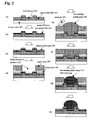
- a wiring board includes a silicon wafer 203 as substrate, and a plurality of electrode pads 201 provided on the substrate surface. Bump-formation apertures 220 are filled with a low-melting metal paste represented by solder paste. A passivation film 202 is formed so as to embed the side surfaces and end surfaces of the electrode pads 201.
- Fig. 2 (a) shows a sectional structure of a semiconductor chip wafer in which the electrode pads 201 are arranged so as to form an area over the entire surface of the semiconductor.
- the wiring board is covered with the passivation film 202 having a thickness of, for example, 1 ⁇ m, so as to expose the major surface of the electrode pads 201.
- an electrode metal diffusion prevention film 204 is formed over the entire surface of the electrode pads 201 and the passivation film 202, by sputtering, deposition or the like.
- the metal diffusion prevention film 204 is formed using any of Ni, Cr, TiN, TaN, Ta, Nb and WN, and in a thickness of, for example, 1 ⁇ m.
- the metal diffusion prevention film 204 may be a single film or a laminated film.
- a barrier metal layer 205 is formed over the entire surface of the wiring board in which the metal diffusion prevention film 204 has been fabricated.
- the barrier metal layer may be produced by depositing a film of a barrier metal selected from Ti, Ni, Pd and Cu in a thickness of several thousands of angstroms with use of a sputtering apparatus or an electron-beam deposition apparatus.
- a laminated two-layer film is formed on the wiring board having the barrier metal layer 205.
- the laminated two-layer film includes a lower layer 206 comprising an alkali-soluble radiation-nonsensitive resin composition and an upper layer 207 comprising a negative radiation-sensitive resin composition.
- the lower layer 206 may be formed by applying a liquid lower layer material in a thickness of 2 to 3 ⁇ m. Thereafter, the upper layer 207 may be formed on the lower layer 206 by applying a liquid negative resist or laminating a negative dry film resist in a thickness of at least 50 ⁇ m.
- the resultant laminated two-layer film consisting of the lower and the upper layers 206 and 207 is irradiated with radiation through a mask and then developed to produce bump-formation apertures 220 at positions that correspond to bump formation positions above the electrode pads 201.
- Possible combinations of the resists, including that in the above process, for forming the laminated two-layer film are for example:
- a low-melting metal paste 208 such as a solder paste, is filled in the bump-formation apertures 220 with use of a squeegee 209 or the like.
- the wiring board with the metal paste filled therein is heated in a nitrogen atmosphere, and the metal paste is reflowed to produce bumps 210.
- the laminated film is peeled as shown in Fig. 2(h).
- the wiring board is then electrically tested and diced into chips.
- the chips are subjected to the flip chip bonding.
- the low-melting metal bumps are produced by filling the metal into the bump-formation apertures 220 with use of the squeegee. It is also possible that the bumps are formed by placement of low-melting metal balls (solder balls) 308 as shown in Fig. 3 (second embodiment) or by electrolytic deposition of a low-melting metal film 408 as shown in Fig. 4 (third embodiment).
- flux cleaning may be performed.
- Figs. 5(a) to (d) explain formation of bumps on a multilayer printed wiring board by the process of the invention.
- Fig. 5 illustrates one conductive circuit and one insulating resin interlayer, pluralities of these circuits and layers are generally present in alternate order.
- a wiring board comprises a substrate 615 comprising glass epoxy resin or BT (bismaleimide-triadine) resin, an insulating resin interlayer 602 overlaid on the substrate, a plurality of electrode pads 605, and a solder resist 611 formed so as to embed the side surfaces of the electrode pads.
- Bump-formation apertures 608 are filled with a low-melting metal paste 610, typically a solder paste, with use of a squeegee.
- Fig. 6 (a) shows a sectional structure of a wiring board in which the electrode pads 605 are arranged so as to form an area over the entire surface of the semiconductor.
- the wiring board used in this embodiment is a multilayer laminated board that includes the insulating resin interlayer 602 and the conductive circuits 603 on the glass epoxy resin 615. The conductance across the thickness of the board is obtained through via holes 604 formed by deposition.
- the solder resist 611 is applied over the insulating resin interlayer 602 and developed to create apertures at positions corresponding to the electrode pads therebelow.
- the conductive circuits 603 are partially exposed at the bottom of the apertures, and the electrode pads 605 are formed on the exposed conductive circuits 603 by electroless deposition.
- a laminated two-layer film is formed on the solder resist 611.
- the laminated two-layer film includes a lower layer 606 comprising an alkali-soluble radiation-nonsensitive resin composition and an upper layer 607 comprising a negative radiation-sensitive resin composition.
- the lower layer 606 may be formed by applying a liquid lower layer material in a thickness of 2 to 3 ⁇ m. Thereafter, the upper layer 607 may be formed on the lower layer 606 by applying a liquid negative resist or laminating a negative dry film resist in a thickness of at least 40 ⁇ m. The resultant laminated film is photoexposed to create a latent pattern and then developed to produce solder-bump-formation apertures 608 at positions that correspond to bump-formation positions above the electrode pads 605.
- a low-melting metal paste 610 such as a solder paste, is filled in the bump-formation apertures 608 with use of a squeegee 609 or the like.
- the wiring board with the metal paste filled therein is heated in a nitrogen atmosphere, and the metal paste is reflowed to produce bumps.
- the laminated film is peeled as shown in Fig. 6(f).
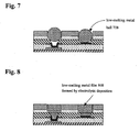
- the low-melting metal bumps are formed by filling the metal into the bump-formation apertures 608 with use of the squeegee. It is also possible that the bumps are formed by placement of low-melting metal balls (solder balls) 708 as shown in Fig. 7 (fifth embodiment) or by electrolytic deposition of a low-melting metal film 808 as shown in Fig. 8 (sixth embodiment).
- flux cleaning may be performed.
- the lower layer is not particularly limited as long as it contains an alkali-soluble compound, preferably an alkali-soluble compound having a phenolic hydroxyl group. Desirably, the lower layer has a composition described below.
- a lower layer material that contains an alkali-soluble radiation-nonsensitive resin composition.
- the lower layer material may be a liquid or a dry film.
- the compounds (A) are broadly divided into low-molecular weight compounds having up to 10 phenol skeletons, and high-molecular weight polymers such as novolak resins and poly(4-hydroxystyrene).
- a developing solution used for forming the apertures is preferably one relatively weak in alkalinity such as sodium carbonate.
- a developing solution used for forming the apertures is preferably one relatively strong in alkalinity such as tetramethylammoniumhydroxide.
- low-molecular weight compounds examples include 4,4'-[1-[4-[1-(4-hydroxyphenyl)-1-methylethyl]phenyl] ethylidene]diphenol, methyl 2,2-bis(1,5-dimethyl-4-hydroxyphenyl)propionate and 4,6-bis[1-(4-hydroxyphenyl)-1-methylethyl]-1,3-benzenediol.
- thermal polymerization inhibitors may also be used. Examples thereof include pyrogallol, benzoquinone, hydroquinone, methylene blue, tert-butylcatechol, monobenzyl ether, methylhydroquinone, amylquinone, amyloxyhydroquinone, n-butylphenol, phenol, hydroquinone monopropyl ether, 4,4'-(1-methylethylidene)bis(2-methylphenol), 4,4'-(1-methylethylidene)bis(2,6-dimethylphenol), 4,4',4''-ethylidene tris(2-methylphenol), 4,4',4''-ethylidene trisphenol and 1,1,3-tris(2,5-dimethyl-4-hydroxyphenyl)-3-phenylpropane.
- high-molecular weight polymers examples include polymers having a phenolic hydroxyl group, such as novolak resins and polyhydroxystyrene described below, and derivatives thereof. They may be used singly or in combination.
- the alkali-soluble novolak resins for use in the invention are condensation products of m-cresol, one or more types of other phenols, and an aldehyde compound.
- the alkali-soluble novolak resins are not particularly limited, provided that the m-cresol has a proportion of 50 to 90 mol% relative to all the phenols.
- Examples of the other types of phenols as materials of the novolak resins include 2,3-xylenol, 2,4-xylenol, 2,5-xylenol, 3,4-xylenol, 3,5-xylenol and 2,3,5-trimethylphenol. These may be used either individually or in combination or two or more kinds.
- m-cresol/phenol(s) combinations include m-cresol/2,3-xylenol, m-cresol/2,4-xylenol, m-cresol/2,3-xylenol/3,4-xylenol, m-cresol/2,3,5-trimethylphenol and m-cresol/2,3-xylenol/2,3,5-trimethylphenol.
- Suitable aldehyde compounds for use in the condensation include formaldehyde, paraformaldehyde, acetaldehyde, benzaldehyde, o-hydroxybenzaldehyde, m-hydroxybenzaldehyde, p-hydroxybenzaldehyde, glyoxal, glutaraldehyde, terephthalaldehyde and isophthalaldehyde.
- formaldehyde and o-hydroxybenzaldehyde are particularly suitable.
- aldehyde compounds may be used either individually or in combination or two or more kinds.
- the aldehyde compound(s) will be used in an amount of 0.4 to 2 mol, and more preferably 0.6 to 1.5 mol per mol of the phenols.
- the condensation between the phenols and the aldehyde compound is usually carried out in the presence of an acid catalyst.
- acid catalysts include hydrochloric acid, nitric acid, sulfuric acid, formic acid, oxalic acid, acetic acid, methanesulfonic acid and p-toluenesulfonic acid.
- the acid catalyst may be used in an amount of 1 ⁇ 10 -5 to 5 ⁇ 10 -1 mol per mol of the phenols.
- the condensation is usually performed using water as reaction medium.
- the water as the reaction medium may be replaced by:
- the reaction medium may be used in an amount of 20 to 1, 000 parts by weight per 100 parts by weight of the reactants.
- condensation temperature may be appropriately adjusted depending on the reactivity of the reactants, it is generally in the range of 10 to 200°C.
- the condensation reaction may be carried out in an appropriate manner.
- the phenols, the aldehyde compound, the acid catalyst, etc. may be introduced into a reactor all at once.
- the phenols, the aldehyde compound, etc. may be added with progress of the reaction in the presence of the acid catalyst.
- the unreacted materials, the acid catalyst, the reaction medium, etc. are removed from the system.
- this can be made through a process in which the temperature in the reaction system is increased to 130 to 230°C and the volatile components are evaporated under reduced pressure to recover the novolak resin.
- Alternative is a process in which the novolak resin obtained is dissolved in a good solvent, followed by mixing with a poor solvent such as water, n-hexane or n-heptane, and the precipitated phase of resin solution is separated to recover the high-molecular weight novolak resin.
- the good solvents include ethylene glycol monomethyl ether acetate, methyl 3-methoxypropionate, ethyl lactate, methyl isobutyl ketone, 2-heptanone, dioxane, methanol and ethyl acetate.
- the novolak resins preferably have a weight-average molecular weight in terms of polystyrene (hereinafter the "Mw") of 2,000 to 20,000, and particularly preferably 3,000 to 15,000, from the viewpoints of workability of the composition into films, and developability, sensitivity and heat resistance of the resulting resist.
- Mw weight-average molecular weight in terms of polystyrene
- Suitable polyhydroxystyrenes for use in the invention include resins commercially available under the trade names of MARUKA LYNCUR M, MARUKA LYNCUR CMM, MARUKA LYNCUR CHM, MARUKA LYNCUR MB, MARUKA LYNCUR PHM-C, MARUKA LYNCUR CST and MARUKA LYNCUR CBA (Maruzen Petrochemical Co., Ltd.).
- a solvent may be employed for dissolving the component A to prepare a coating solution.
- the solvents are not particularly limited as long as the component A is favorably dissolved therein.
- examples thereof include ethylene glycol monomethyl ether, ethylene glycol monoethyl ether, ethylene glycol monomethyl ether acetate, ethylene glycol monoethyl ether acetate, diethylene glycol monomethyl ether, diethylene glycol monoethyl ether, propylene glycol monomethyl ether acetate, propylene glycol monopropyl ether acetate, toluene, xylene, methyl ethyl ketone, 2-heptanone, 3-heptanone, 4-heptanone, cyclohexanone, ethyl 2-hydroxypropionate, ethyl 2-hydroxy-2-methylpropionate, ethyl ethoxyacetate, ethyl hydroxyacetate, methyl 2-hydroxy-3-methylbutanoate, methyl 3-
- high-boiling solvents such as N-methylformamide, N,N-dimethylformamide, N-methylformanilide, N-methylacetamide, N,N-dimethylacetamide, N-methylpyrrolidone, dimethyl sulfoxide, benzyl ethyl ether, dihexyl ether, acetonylacetone, isophorone, caproic acid, caprylic acid, 1-octanol, 1-nonanol, benzyl alcohol, benzyl acetate, ethyl benzoate, diethyl oxalate, diethyl maleate, ⁇ -butyrolactone, ethylene carbonate, propylene carbonate and ethylene glycol monophenyl ether acetate.
- These solvents may be used singly or in combination of two or more kinds. Of these, ethyl 2-hydroxypropionate and propylene glycol monomethyl ether acetate are preferable.
- An alkali-soluble acrylic resin may be added in order to improve application properties and to stabilize coating film properties, particularly when the component A is the low-molecular weight compound having a phenolic hydroxyl group.
- the composition of the acrylic resin is not particularly limited, provided that the resin contains a unit derived from a (meth) acrylic ester, and a unit imparting alkali solubility that is derived from a radically polymerizable compound having a carboxyl group and/or a phenolic hydroxyl group.
- Examples of the radically polymerizable compounds having a carboxyl group include acrylic acid and methacrylic acid.
- Examples of the radically polymerizable compounds having a phenolic hydroxyl group include vinyl monomers having a phenolic hydroxyl group, such as p-hydroxystyrene, m-hydroxystyrene, o-hydroxystyrene, ⁇ -methyl-p-hydroxystyrene, ⁇ -methyl-m-hydroxystyrene, ⁇ -methyl-o-hydroxystyrene, 4-isopropenylphenol, 2-allylphenol, 4-allylphenol, 2-allyl-6-methylphenol, 2-allyl-6-methoxyphenol, 4-allyl-2-methoxyphenol, 4-allyl-2,6-dimethoxyphenol and 4-allyloxy-2-hydroxybenzophenone. These compounds may be used either individually or in combination of two or more kinds. Of the compounds, p-hydroxystyrene and 4-isopropenylphenol are preferred.
- the acrylic copolymer contains 1 to 60 wt%, preferably 5 to 50 wt% the unit derived from the carboxyl-containing radically polymerizable compound and/or the unit derived from the phenolic hydroxyl-containing radically polymerizable compound.
- the acrylic copolymer becomes less soluble in the alkaline developing solution, so that the developing results in residual film and poor resolution.
- the acrylic copolymer has too high a solubility in the alkaline developing solution, so that the two-layer film will have apertures with undercuts.
- a surfactant may be added to the composition in order to improve application, defoaming and leveling properties.
- Suitable surfactants include fluorine-containing surfactants commercially available under the trade names of BM-1000 and BM-1100 (manufactured by BM Chemie); MEGAFACE series F142D, F172, F173 and F183 (manufactured by Dainippon Ink and Chemicals, Incorporated); FLUORAD series FC-135, FC-170C, FC-430 and FC-431 (manufactured by Sumitomo 3M); SURFLON series S-112, S-113, S-131, S-141 and S-145 (manufactured by Asahi Glass Co., Ltd.); and SH-28PA, SH-190, SH-193, SZ-6032 and SF-8428 (manufactured by Toray Dow Corning Silicone Co., Ltd.).
- the amount of the surfactant is preferably not more than 5 parts by weight per 100 parts by weight of
- the lower layer material may contain other components.
- Specific examples thereof include phenol novolak epoxy resins, cresol novolak epoxy resins, bisphenol epoxy resins, trisphenol epoxy resins, tetraphenol epoxy resins, phenol-xylylene epoxy resins, naphthol-xylylene epoxy resins, phenol-naphthol epoxy resins, phenol-dicyclopentadiene epoxy resins and alicyclic epoxy resins.
- Inorganic fillers are also employable. Specific examples of the inorganic fillers include silica, aluminum hydroxide and barium sulfate.
- Other employable additives are polymer additives, reactive diluents, leveling agents, wettability improvers, plasticizers, antioxidants, antistatic agents, mildew-proofing agents, moisture conditioners and flame-retardants.
- an upper layer material that contains a negative radiation-sensitive resin composition.
- the upper layer material may be a liquid or a dry film.
- the radiation-sensitive resin compositions as described in JP-A-H08-301911 may be employed as the negative radiation-sensitive resin composition.
- the negative radiation-sensitive resin composition used in the invention includes an acrylic resin (the above component C), a crosslinking agent (component E), an initiator (component F), a solvent (the above component B), and a surfactant (the above component D).
- Exemplary crosslinking agents include trimethylolpropane tri(meth)acrylate, pentaerythritol tri(meth)acrylate, ethylene glycol di(meth)acrylate, tetraethylene glycol di(meth)acrylate, polyethylene glycol di(meth)acrylate, 1,4-butanediol di(meth)acrylate, butylene glycol di (meth) acrylate, propylene glycol di(meth)acrylate, trimethylolpropane di(meth)acrylate, 1,6-hexanediol di(meth)acrylate, neopentyl glycol di(meth)acrylate, trimethylolpropane tri(meth)acrylate, tris(2-hydroxyethyl)isocyanurate tri(meth)acrylate, tris(2-hydroxyethyl)isocyanurate di(meth)acrylate, tricyclodecanedimethanol di(meth)
- crosslinking agents may be used as the crosslinking agents (components E).
- examples thereof include compounds commercially available under the trade names of ARONIX series M-210, M-309, M-310, M-400, M-7100, M-8030, M-8060, M-8100, M-9050, M-240, M-245, M-6100, M-6200, M-6250, M-6300, M-6400 and M-6500 (manufactured by Toagosei Co., Ltd.); KAYARAD series R-551, R-712, TMPTA, HDDA, TPGDA, PEG400DA, MANDA, HX-220, HX-620, R-604, DPCA-20, DPCA-30, DPCA-60 and DPCA-120 (manufactured by Nippon Kayaku Co., Ltd.); and Biscoat series Nos. 295, 300, 260, 312, 335HP, 360, GPT, 3PA and 400 (manufactured by Osaka Organic Chemical Industry Ltd
- crosslinking agents may be used singly or in combination of two or more kinds.
- the crosslinking agent is used in an amount of 10 to 250 parts by weight, more preferably 20 to 200 parts by weight, and particularly preferably 25 to 150 parts by weight per 100 parts by weight of the acrylic resin (component C).
- the amount is less than 10 parts by weight, the photosensitivity tends to be lowered.
- the amount exceeds 250 parts by weight, the compatibility with the copolymer (A) will be deteriorated, leading to poor storage stability and difficulties in achieving the film thickness of 20 ⁇ m or more.
- the radiation-induced radical polymerization initiators for use in the invention include ⁇ -diketones such as benzyl and diacetyl; acyloins such as benzoin; acyloin ethers such as benzoin methyl ether, benzoin ethyl ether and benzoin isopropyl ether; benzophenones such as thioxanthone, 2,4-diethyl thioxanthone, thioxanthone-4-sulfonic acid, benzophenone, 4,4'-bis(dimethylamino)benzophenone and 4,4'-bis(diethylamino)benzophenone; acetophenones such as acetophenone, p-dimethylaminoacetophenone, ⁇ , ⁇ -dimethoxy- ⁇ -acetoxybenzophenone, ⁇ , ⁇ -dimethoxy- ⁇ -phenylacetophen
- initiators include IRGACURE series 184, 651, 500, 907, CGI369 and CG24-61 (manufactured by Ciba Specialty Chemicals Inc.); LUCIRIN LR8728 and LUCIRIN TPO (manufactured by BASF); DAROCUR series 1116 and 1173 (manufactured by Ciba Specialty Chemicals Inc.); and UBECRYL P36 (manufactured by UCB).
- the above radiation-induced radical polymerization initiators may be used in combination with hydrogen donor compounds such as mercaptobenzothiazole and mercaptobenzoxazole.
- acetophenones such as 1-[2-methyl-4-methylthiophenyl]-2-morpholino-1-propanone, 2-benzyl-2-dimethylamino-1-(4-morpholinophenyl)-butane-1-one and ⁇ , ⁇ -dimethoxy- ⁇ -phenylacetophenone; phenacyl chloride and tribromomethylphenylsulfone; 2,4,6-trimethylbenzoyldiphenylphosphine oxide; combinations of the 1,2'-bisimidazoles and 4,4'-diethylaminobenzophenone and mercaptobenzothiazole; LUCIRIN TPO; and IRGACURE 651.
- the initiator is used in an amount of 0.1 to 60 parts by weight, more preferably 5 to 50 parts by weight, and particularly preferably 10 to 40 parts by weight per 100 parts by weight of the alkali-soluble copolymer (A).
- the amount is less than 1 wt%, radicals are more liable to be deactivated by oxygen (leading to deteriorated sensitivity).
- the amount exceeding 60 wt% tends to cause poor compatibility and low storage stability.
- the radiation-induced radical polymerization initiators may be used in combination with radiation sensitizers.
- the lower layer is formed by application or lamination, and thereafter the upper layer is formed by application or lamination.
- a desired laminated two-layer film may be produced.
- the application may be performed by dipping, spin coating, roll coating or screen process printing, or by use of an applicator or a curtain coater.
- lamination or vacuum lamination may be adopted. Drying conditions for the lower and upper layers vary depending on the kinds and proportions of the components making up the composition and the coating thickness. Generally, the drying is performed at temperatures in the range of 70 to 120°C, and preferably 80 to 100°C, for about 5 to 20 minutes. When the drying time is too short, adhesion may be bad at the time of development. Any overlong drying causes an excessive thermal change that leads to lowering of the resolution.
- the lower layer material and the upper layer material are in advance formed into a two-layer dry film and laminated on the substrate.
- the laminated film obtained as described above is then irradiated with ultraviolet rays or visible rays of 300 to 500 nm wavelength, through a photomask having a desired pattern.
- exemplary radiation sources include low-pressure, high-pressure and super-high-pressure mercury lamps, metal halide lamps and argon gas lasers.
- the radiations include ultraviolet rays, visible rays, far ultraviolet rays, X-rays and electron beams.
- the dose of radiation varies depending on the kinds and proportions of the components making up the composition and the film thickness; for example, it is in the range of 100 to 500 mJ/cm 2 in the case of super-high-pressure mercury lamps.
- alkaline aqueous solutions include alkaline aqueous solutions of sodium hydroxide, potassium hydroxide, sodium carbonate, sodium silicate, sodium metasilicate, aqueous ammonia, ethylamine, n-propylamine, diethylamine, di-n-propylamine, triethylamine, methyldiethylamine, dimethylethanolamine, triethanolamine, tetramethylammonium hydroxide, tetraethylammonium hydroxide, pyrrole, piperidine, 1,8-diazabicyclo[5.4.0]-7-undecene and 1,5-diazabicyclo[4.3.0]-5-nonane.
- the developing solution may be a mixture of the above alkaline aqueous solution and an appropriate amount of a water-soluble organic solvent, such as methanol or ethanol, or a surfactant.
- the development time varies depending on the kinds and proportions of the components making up the composition and the film thickness; for example, it is usually in the range of 30 to 360 seconds.
- the developing method may be any of dropping, dipping, paddling and spraying. After the development, the patterned film is washed under running water for 30 to 90 seconds and thereafter air dried using an air gun or dried in an oven.
- the irradiated area of the upper layer is left and the lower layer is dissolved and removed correspondingly to the removed area (non-irradiated area) of the upper layer.
- the remaining resist layers may be subjected to post photoexposure or heating to be further cured.
- the low-melting metal such as solder paste is filled in the aperture pattern as described above, and the metal is reflowed to form bumps.
- the low-melting metal may be filled in the aperture pattern by direct placement of solder balls or electrolytic deposition.
- the cured layers (resist layers) remaining on the substrate are peeled.
- the peeling may be performed by, for example, immersing the substrate in a peeling solution at 50 to 80°C with agitation for 5 to 30 minutes.
- Preferred peeling solutions used herein include dimethyl sulfoxide, and a mixed solution of quaternary ammonium salt, dimethyl sulfoxide and water.
- the laminated two-layer film may be peeled and removed from the substrate with use of a peeling apparatus having multistage immersion baths.
- the treatment may be designed to peel the laminated two-layer film in the first bath containing an appropriate organic solvent, followed by cycle filtration of the peeled pieces, and to peel the residual laminated film in the second and later baths filled with a peeling solution containing an organic alkali component.
- the treatment may be preferably designed to peel the laminated two-layer film in the first bath containing dimethyl sulfoxide, followed by cycle filtration of the peeled pieces, and to peel the residual laminated film in the second and later baths filled with a peeling solution containing an organic alkali component and dimethyl sulfoxide.
- part(s) and % refer to part(s) by weight and % by weight.
- a flask equipped with a dry ice/methanol reflux condenser and a thermometer was purged with nitrogen.
- the flask was then charged with 4.0 g of 2,2'-azobisisobutyronitrile as polymerization initiator, and 120 g of ethyl 2-hydroxypropionate as solvent. They were stirred until the polymerization initiator was dissolved in the solvent.
- 20.0 g of acrylic acid, 10.0 g of p-isopropenylphenol, 30.0 g of n-butyl methacrylate, 20.0 g of methyl methacrylate and 20.0 g of n-butyl acrylate were introduced into the flask. The contents were stirred slowly to give a solution.
- the solution was then heated to 80°C, and polymerization was carried out at the temperature for 4 hours.
- the solution temperature was raised to 100°C and polymerization was performed at the temperature for 1 hour. Thereafter, the solution was allowed to cool to room temperature, and the gas in the flask was replaced with air.
- the solution obtained by the above reaction was added dropwise to a large quantity of methanol to coagulate the reaction product.
- the coagulated product was washed with water, redissolved in tetrahydrofuran of the same weight as the coagulated product, and recoagulated in a large amount of methanol.
- the operation of redissolution through recoagulation was carried out three times in total.
- the coagulated product thus obtained was vacuum dried at 40°C for 48 hours to yield an acrylic resin C-1.
- the solution was then heated to 70°C, and polymerization was carried out at the temperature for 3 hours. After addition of 1.5 g of the polymerization initiator 2,2'-azobisisobutyronitrile, polymerization was conducted at 70°C for 3 hours. Thereafter, the solution was allowed to cool to room temperature, and the gas in the flask was replaced with air, followed by addition of 150 mg of p-methoxyphenol.
- the solution obtained by the above reaction was added dropwise to a large quantity of methanol to coagulate the reaction product.
- the coagulated product was washed with water, redissolved in tetrahydrofuran of the same weight as the coagulated product, and recoagulated in a large amount of methanol. The operation of redissolution through recoagulation was carried out three times in total.
- the coagulated product thus obtained was vacuum dried at 40°C for 48 hours to yield an acrylic resin C-3.
- Dry films were prepared from the lower layer materials B-L and C-L, as follows.
- the lower layer material B-L was spin coated over an 11 cm-square polyethyleneterephthalate (PET) film having a thickness of 50 ⁇ m so that the post baking film thickness would be 5 ⁇ m.
- PET polyethyleneterephthalate
- the coating was baked in a convection oven at 110°C for 10 minutes to give a lower layer material B-D.
- a lower layer material C-D was produced in a similar manner.
- Dry films were prepared from the upper layer materials A-L and B-L, as follows.
- the upper layer material A-L was spin coated over an 11 cm-square polyethyleneterephthalate (PET) film having a thickness of 50 ⁇ m so that the post baking film thickness would be 40 ⁇ m.
- PET polyethyleneterephthalate
- the coating was baked in a convection oven at 110°C for 10 minutes to give an upper layer material A-D.
- An upper layer material B-D was produced in a similar manner.
- Two-layer dry films were prepared from combinations shown in Table 3, as follows.
- the upper layer material B-L was spin coated over an 11 cm-square polyethyleneterephthalate (PET) film having a thickness of 50 ⁇ m so that the post baking film thickness would be 40 ⁇ m.
- PET polyethyleneterephthalate
- the coating was baked in a convection oven at 110°C for 10 minutes.
- the lower layer material B-L was spin coated over the coated substrate so that the post baking film thickness would be 40 ⁇ m.
- the coating was baked in a convection oven at 110°C for 10 minutes.
- a two-layer dry film B was prepared in a similar manner.
- a peeling solution 1 was prepared by adding 100 g of an aqueous tetramethylammoniumhydroxide solution (25 wt%) to 4900 g of dimethyl sulfoxide, followed by stirring.
- an evaluation board A was prepared.
- a surface-roughened, copper-clad glass epoxy laminate (substrate thickness: 0.6 mm, size: 10 cm square) was coated with a solder resist (product of JSR, the photosensitive insulating resin composition described in Example 1 of Japanese Patent Application No. 2000-334348).
- the solder resist contained (i) a cresol novolak resin containing m-cresol and p-cresol in a molar ratio of 60/40 (weight-average molecular weight in terms of polystyrene: 8700), (ii) hexamethoxymethylmelamine, (iii) crosslinked fine particles, (iv) styryl-bis(trichloromethyl)-s-triadine, and (v) ethyl lactate as solvent.
- the coating was heated in a convection oven at 90°C for 10 minutes to give a uniform film having a thickness of 30 ⁇ m.
- the film was photoexposed through a pattern mask with ultraviolet rays from a high-pressure mercury lamp with use of an aligner (MA-150, available from Suss Microtech Inc.) in a manner such that the dose was in the range of 300 to 500 mJ/cm 2 at a wavelength of 350 nm.
- PEB post exposure baking
- the film was then developed by being showered with a 1-wt% sodium hydroxide aqueous solution having a temperature of 30°C over a period of 2 to 3 minutes (pressure: 3 kgf ⁇ cm 2 ).
- the developed film was photoexposed in a dose of 1000 mJ/cm 2 at 350 nm wavelength with use of a high-pressure mercury lamp, and was subsequently heated in a convection oven at 150°C for 2 hours and at 170°C for 2 hours. Thus, a cured film was produced.
- the board thus obtained had a first aperture pattern which was a combination of:
- the apertures of the board were electroless plated with Ni and Au. An evaluation board B was thus obtained.
- the liquid lower layer material or upper layer material was directly dropped on the evaluation board, and was spread by means of a spin coater so as to achieve a post baking film thickness of 40 ⁇ m.
- the coating was baked in a convection oven at 110°C for 10 minutes.
- the coated board was gradually cooled to room temperature, and the coated surface was covered with a 50 ⁇ m thick PET film with use of a laminator.
- the dry-film lower layer and upper layer materials, or the two-layer dry film was laminated on the board with use of a laminator.
- the PET film substrate was left unreleased.
- the lower layer material A-L was spin coated over the evaluation board A, and the coating was baked on a hot plate at 120°C for 5 minutes to give a lower layer 5 ⁇ m thick.
- the upper layer material A-L was spin coated, and the coating was baked on a hot plate at 120°C for 5 minutes to give an upper layer having a thickness of 65 ⁇ m.
- the laminated film was photoexposed through a patterned glass mask with ultraviolet rays from a high-pressure mercury lamp with use of an aligner (MA-150, available from Suss Microtech Inc.) in a manner such that the dose was 1000 mJ/cm 2 at a wavelength of 420 nm.
- an aligner MA-150, available from Suss Microtech Inc.
- the glass mask was brought into intimate contact with the board covered with the PET film.
- TMAH developing solution aqueous solution containing 2.38% tetramethylammoniumhydroxide
- the developer application time was generally 90 seconds and adjusted by 15 seconds.
- the board was rinsed with ion-exchange water for 60 seconds.
- the patterned board had a plurality of hole patterns of 75 ⁇ m x 75 ⁇ m apertures.
- solder paste used herein contained Sn and Ag in a weight ratio of 96.5:3.5 and contained solder particles 5 to 20 ⁇ m in diameter. The viscosity thereof had been adjusted to 200 Pa ⁇ s. Thereafter, the solder paste was removed using a squeegee from the surface other than within the solder-bump formation apertures. The paste was completely removed with cleaning paper, and the surface of the solder paste was flattened.
- solder paste printed in the above step was reflowed at 250°C, followed by flux cleaning.
- the board was cooled to room temperature. Separately, approximately 1 liter of dimethyl sulfoxide or the peeling solution 1 was placed in a peeling bath and heated to about 60°C. The board was immersed in the bath for 10 minutes under agitation, and thereby the laminated two-layer film was peeled.
- the board having been peeling treated in the peeling bath was rinsed with isopropyl alcohol and washed with water, and was dried using an air gun.
- the lower layer material A-L was spin coated over the evaluation board A, and the coating was baked on a hot plate at 120°C for 5 minutes to give a lower layer 5 ⁇ m thick.
- the upper layer material A-D (thickness: 65 ⁇ m) was laminated.
- the lower layer material B-L was spin coated over the evaluation board B, and the coating was baked in a clean oven at 110°C for 10 minutes to give a lower layer 2 ⁇ m thick.
- the upper layer material B-L was spin coated, and the coating was baked at 110°C for 10 minutes to give an upper layer having a thickness of 40 ⁇ m.
- the laminated film was photoexposed through a patterned glass mask with ultraviolet rays from a high-pressure mercury lamp with use of an aligner (MA-150, available from Suss Microtech Inc.) in a manner such that the dose was 400 mJ/cm 2 at a wavelength of 350 nm.
- an aligner MA-150, available from Suss Microtech Inc.
- the glass mask was brought into intimate contact with the board covered with the PET film.
- the hole pattern (first aperture pattern) of the evaluation board was aligned with a second aperture pattern of the radiation-sensitive resin composition.
- the above-photoexposed board was subjected to development by being showered with a 1 wt% sodium carbonate aqueous solution having a temperature of 30°C (pressure: 1 kgf ⁇ cm 2 ).
- the showering time was generally 45 seconds and adjusted by 15 seconds.
- First aperture pattern Second aperture pattern 150 ⁇ m pitch 95 ⁇ m-diameter holes 100 ⁇ m-diameter holes 125 ⁇ m pitch 80 ⁇ m-diameter holes 90 ⁇ m-diameter holes 100 ⁇ m pitch 60 ⁇ m-diameter holes 80 ⁇ m-diameter holes
- the lower layer material B-L was spin coated over the evaluation board B, and the coating was baked on a hot plate at 120°C for 5 minutes to give a lower layer 2 ⁇ m thick.
- the upper layer material B-D (thickness: 40 ⁇ m) was laminated.
- the lower layer material B-L was spin coated over the evaluation board B, and the coating was baked in a clean oven at 110°C for 10 minutes to give a lower layer 2 ⁇ m thick.
- the upper layer material A-L was spin coated, and the coating was baked in a clean oven at 110°C for 10 minutes to give an upper layer having a thickness of 40 ⁇ m.
- the photoexposed board was subjected to development by being showered with a 1% sodium hydroxide aqueous solution (hereinafter, abbreviated as NaOH developing solution) having a temperature of 30°C (pressure: 1 kgf ⁇ cm 2 ).
- the showering time was generally 45 seconds and adjusted by 15 seconds.
- the board was rinsed with ion-exchange water for 60 seconds.
- the lower layer material B-L was spin coated over the evaluation board B, and the coating was baked on a hot plate at 120°C for 5 minutes to give a lower layer 2 ⁇ m thick.
- the upper layer material B-D (thickness: 40 ⁇ m) was laminated.
- the lower layer material B-D was laminated on the evaluation board B to provide a lower layer of 2 ⁇ m thickness.
- the upper layer material B-L was spin coated, and the coating was baked in a clean oven at 110°C for 10 minutes to give an upper layer having a thickness of 40 ⁇ m.
- the lower layer material B-D was laminated on the evaluation board B to provide a lower layer of 2 ⁇ m thickness.
- the upper layer material B-D (thickness: 40 ⁇ m) was laminated.
- the two-layer dry film A was laminated on the evaluation board B.
- the two-layer dry film B was laminated on the evaluation board B.
- Comparative Examples 1 to 4 were carried out in the same manner as in Examples bearing the corresponding number, except that no lower layer was provided.
Landscapes
- Engineering & Computer Science (AREA)
- Manufacturing & Machinery (AREA)
- Microelectronics & Electronic Packaging (AREA)
- Materials For Photolithography (AREA)
- Photosensitive Polymer And Photoresist Processing (AREA)
- Wire Bonding (AREA)
Abstract
A process for forming bumps on electrode pads performs
at least the following steps (a) to (d) for a wiring board
including a substrate and a plurality of electrode pads:

Description
The present invention relates to a process for forming
low-melting metal bumps such as solder bumps used in the
mounting of IC chips on a multilayer printed wiring board.
Low-melting metal bumps such as solder bumps are used
for the mounting of IC chips and the like. Formation of such
bumps takes place on the IC chips or on the multilayer printed
wiring board.
BGA (ball grid array) is a form of package in which the
bumps are provided to an IC chip. This term generally refers
to a package in which the IC chip is mounted on a package
substrate.
WL-CSP (wafer level-chip size packaging) is a new
technology for the high-density mounting. In the WL-CSP, a
plurality of IC chip circuits is formed on one wafer and
collectively subjected to electrode formation, packaging and
burn-in test; thereafter the wafer is cut into IC chip packages.
Collective electrode formation in the WL-CSP may be
performed by electrolytic deposition, filling a metal paste
followed by reflowing, or placing metal balls followed by
reflowing.
The increase of IC chip density has lead to higher density
and miniaturization of bumps on the IC chip. Solder bumps have
increasingly been studied and been in practical use in the
WL-CSP mounting technology because they allow both connection
reliability and reduction of processing cost. Specifically,
the solder bumps are formed by electrolytic deposition using
a mask that is produced by patterning a film of at least 50
µm thickness formed by application or lamination of a positive
or negative liquid resist or dry film.
Meanwhile, when the solder bumps are provided to a
multilayer printed wiring board, a solder resist layer is
formed on the wiring board to prevent fusion bonding between
the solder bumps. The solder resist layer is provided with
apertures at positions corresponding to electrode pads. To
form the solder bumps in the solder resist layer, mask printing
of a solder paste is performed. The mask used in the mask
printing has a pattern (pattern of apertures) that corresponds
to the apertures of the solder resist layer. In carrying out
the mask printing, the mask is placed on the solder resist layer
so as to align the mask pattern and the apertures of the solder
resist layer. The solder paste is then printed through the
mask within the apertures of the solder resist layer on the
electrode pads; subsequently, the solder paste is reflowed to
form solder bumps on the electrode pads.
A variety of studies have been made to cope with reduction
of solder bump pitches. For example, JP-A-H10-350230
discloses formation of a peelable solder dam resist on a solder
resist, and JP-A-2000-208911 discloses a method wherein a dry
film is laminated on the solder resist layer, apertures are
created at positions corresponding to electrode pads, a solder
paste is applied followed by reflowing, and the dry film is
peeled.
In the aforementioned process of bump formation, the
positive resist, although easily peelable in general, causes
difficult control of the aperture pattern configuration, often
resulting in nonuniform bump size.
On the other hand, the negative resist permits relatively
easy control of pattern shape, but is generally difficult to
peel because of its photocrosslinking characteristics. In
particular, when the solder bumps are formed by filling and
reflowing the paste, the resist becomes even more difficult
to peel from the board because the crosslinking in the negative
resist proceeds to a further extent by the heat applied in the
reflowing.
The resist film peeling is generally performed by spray
method with an aqueous solution of sodium hydroxide or sodium
carbonate. For the dry-film or liquid negative resist, dip
method has been increasingly employed with use of a peeling
solution that contains a highly polar solvent and an organic
alkali. The former method, although inexpensive, often
results in residual resist around the bumps having a high
density, and causes deterioration of the bumps. The latter
method has disadvantages that the peeling solution is
expensive, and the metal surface of the bumps and the underlying
board surface are corroded when the organic alkali
concentration and the peeling solution temperature are
increased for improving the peeling efficiency per amount of
the peeling solution.
The present invention has been made to solve the
aforesaid problems. As shown in Figs. 1(a) and 5(a), a
laminated two-layer film is formed on a wiring board, which
two-layer film includes a lower layer comprising an
alkali-soluble radiation-nonsensitive resin composition and
an upper layer comprising a negative radiation-sensitive resin
composition. Thereafter, photoexposure and development are
performed one time to create a pattern of apertures for bump
formation at positions corresponding to electrode pads.
The laminated film of the invention includes two layers
having different properties, so that both high resolution and
easy peeling property are achieved. Namely, the use of the
lower layer that comprises a compound having a phenolic
hydroxyl group leads to the following effects:
Accordingly, the negative resist traditionally
unsuitable for use due to poor peelability can be used as upper
layer. The use of the negative resist as the upper layer
permits sufficient mechanical strength of the resist pattern
required in the step of filling a low-melting metal into the
bump-formation aperture pattern as illustrated in Fig. 1(b)
or 5(b).
Furthermore, the lower layer has excellent peelability
such that it can be peeled even by single use of a highly polar
organic solvent such as dimethyl sulfoxide or
N-methylpyrrolidone. The peeled pieces have the upper layer
that has been crosslinked and is hardly soluble in such highly
polar organic solvents. Accordingly, the peeled pieces can
be easily removed by precipitation separation or cycle
filtration.
When the peel treatment employs a peeling apparatus
having multistage immersion baths, the treatment may be
designed to peel most of the negative resist film in the first
bath containing the organic solvent, and to remove the residues
of the lower layer in the second and later baths filled with
a peeling solution containing an alkali component. Thus, the
peeling efficiency can be improved without increasing the
alkali concentration of the peeling solution, and the damage
to the solder bumps and the underlying board can be minimized.
Hereinbelow, the process of bump formation according to
the present invention will be described with reference to the
drawings.
A first embodiment of the process for forming bumps on
electrode pads according to the invention will be explained
in great detail with reference to Fig. 2. In the present
embodiment, a wiring board includes a silicon wafer 203 as
substrate, and a plurality of electrode pads 201 provided on
the substrate surface. Bump-formation apertures 220 are
filled with a low-melting metal paste represented by solder
paste. A passivation film 202 is formed so as to embed the
side surfaces and end surfaces of the electrode pads 201.
Fig. 2 (a) shows a sectional structure of a semiconductor
chip wafer in which the electrode pads 201 are arranged so as
to form an area over the entire surface of the semiconductor.
When the electrode pads 201 have been formed on the silicon
wafer 203, the wiring board is covered with the passivation
film 202 having a thickness of, for example, 1 µm, so as to
expose the major surface of the electrode pads 201.
As illustrated in Fig. 2 (b), an electrode metal diffusion
prevention film 204 is formed over the entire surface of the
electrode pads 201 and the passivation film 202, by sputtering,
deposition or the like. The metal diffusion prevention film
204 is formed using any of Ni, Cr, TiN, TaN, Ta, Nb and WN,
and in a thickness of, for example, 1 µm. The metal diffusion
prevention film 204 may be a single film or a laminated film.
As illustrated in Fig. 2(c), a barrier metal layer 205
is formed over the entire surface of the wiring board in which
the metal diffusion prevention film 204 has been fabricated.
The barrier metal layer may be produced by depositing a film
of a barrier metal selected from Ti, Ni, Pd and Cu in a thickness
of several thousands of angstroms with use of a sputtering
apparatus or an electron-beam deposition apparatus.
As shown in Fig. 2(d), a laminated two-layer film is
formed on the wiring board having the barrier metal layer 205.
The laminated two-layer film includes a lower layer 206
comprising an alkali-soluble radiation-nonsensitive resin
composition and an upper layer 207 comprising a negative
radiation-sensitive resin composition.
For example, the lower layer 206 may be formed by applying
a liquid lower layer material in a thickness of 2 to 3 µm.
Thereafter, the upper layer 207 may be formed on the lower layer
206 by applying a liquid negative resist or laminating a
negative dry film resist in a thickness of at least 50 µm. The
resultant laminated two-layer film consisting of the lower and
the upper layers 206 and 207 is irradiated with radiation
through a mask and then developed to produce bump-formation
apertures 220 at positions that correspond to bump formation
positions above the electrode pads 201.
Possible combinations of the resists, including that in
the above process, for forming the laminated two-layer film
are for example:
As illustrated in Fig. 2(e), a low-melting metal paste
208, such as a solder paste, is filled in the bump-formation
apertures 220 with use of a squeegee 209 or the like.
Referring to Figs. 2(f) and (g), the wiring board with
the metal paste filled therein is heated in a nitrogen
atmosphere, and the metal paste is reflowed to produce bumps
210.
Subsequently, the laminated film is peeled as shown in
Fig. 2(h). The wiring board is then electrically tested and
diced into chips. The chips are subjected to the flip chip
bonding.
Although the above-described embodiment employs a
solder paste as the low-melting metal paste, good reliability
may be obtained by use of a mixture of metals such as Sn, Pb,
Ag, Bi, Zn, In, Sb, Cu, Bi and Ge. In the above embodiment,
the low-melting metal bumps, preferably solder bumps, are
produced by filling the metal into the bump-formation
apertures 220 with use of the squeegee. It is also possible
that the bumps are formed by placement of low-melting metal
balls (solder balls) 308 as shown in Fig. 3 (second embodiment)
or by electrolytic deposition of a low-melting metal film 408
as shown in Fig. 4 (third embodiment).
After the metal paste is reflowed, flux cleaning may be
performed.
Figs. 5(a) to (d) explain formation of bumps on a
multilayer printed wiring board by the process of the invention.
Although Fig. 5 illustrates one conductive circuit and one
insulating resin interlayer, pluralities of these circuits and
layers are generally present in alternate order.
A fourth embodiment of the process for forming bumps on
electrode pads according to the invention will be explained
with reference to Fig. 6. In the present embodiment, a wiring
board comprises a substrate 615 comprising glass epoxy resin
or BT (bismaleimide-triadine) resin, an insulating resin
interlayer 602 overlaid on the substrate, a plurality of
electrode pads 605, and a solder resist 611 formed so as to
embed the side surfaces of the electrode pads. Bump-formation
apertures 608 are filled with a low-melting metal paste 610,
typically a solder paste, with use of a squeegee.
Fig. 6 (a) shows a sectional structure of a wiring board
in which the electrode pads 605 are arranged so as to form an
area over the entire surface of the semiconductor. The wiring
board used in this embodiment is a multilayer laminated board
that includes the insulating resin interlayer 602 and the
conductive circuits 603 on the glass epoxy resin 615. The
conductance across the thickness of the board is obtained
through via holes 604 formed by deposition. The solder resist
611 is applied over the insulating resin interlayer 602 and
developed to create apertures at positions corresponding to
the electrode pads therebelow. The conductive circuits 603
are partially exposed at the bottom of the apertures, and the
electrode pads 605 are formed on the exposed conductive
circuits 603 by electroless deposition.
As shown in Fig. 6(b), a laminated two-layer film is
formed on the solder resist 611. The laminated two-layer film
includes a lower layer 606 comprising an alkali-soluble
radiation-nonsensitive resin composition and an upper layer
607 comprising a negative radiation-sensitive resin
composition.
For example, the lower layer 606 may be formed by applying
a liquid lower layer material in a thickness of 2 to 3 µm.
Thereafter, the upper layer 607 may be formed on the lower layer
606 by applying a liquid negative resist or laminating a
negative dry film resist in a thickness of at least 40 µm. The
resultant laminated film is photoexposed to create a latent
pattern and then developed to produce solder-bump-formation
apertures 608 at positions that correspond to bump-formation
positions above the electrode pads 605.
Similarly to the aforementioned embodiment using the
silicon wafer substrate, possible combinations of the resists,
including that in the above process, for forming the laminated
two-layer film are for example:
As illustrated in Fig. 6(c), a low-melting metal paste
610, such as a solder paste, is filled in the bump-formation
apertures 608 with use of a squeegee 609 or the like.
Referring to Figs. 6(d) and (e), the wiring board with
the metal paste filled therein is heated in a nitrogen
atmosphere, and the metal paste is reflowed to produce bumps.
Subsequently, the laminated film is peeled as shown in
Fig. 6(f).
Although the above-described embodiment employs a
solder paste as the low-melting metal paste, good reliability
may be obtained by use of a mixture of metals such as Sn, Pb,
Ag, Bi, Zn, In, Sb, Cu, Bi and Ge. In the above embodiment,
the low-melting metal bumps, preferably solder bumps, are
formed by filling the metal into the bump-formation apertures
608 with use of the squeegee. It is also possible that the
bumps are formed by placement of low-melting metal balls
(solder balls) 708 as shown in Fig. 7 (fifth embodiment) or
by electrolytic deposition of a low-melting metal film 808 as
shown in Fig. 8 (sixth embodiment).
After the metal paste is reflowed, flux cleaning may be
performed.
Hereinbelow, materials of the lower and upper layers for
use in the present invention will be described.
The lower layer is not particularly limited as long as
it contains an alkali-soluble compound, preferably an
alkali-soluble compound having a phenolic hydroxyl group.
Desirably, the lower layer has a composition described below.
For the formation of the lower layer, a lower layer
material is used that contains an alkali-soluble
radiation-nonsensitive resin composition. The lower layer
material may be a liquid or a dry film.
The above title compounds (hereinafter, the compounds
(A)) are broadly divided into low-molecular weight compounds
having up to 10 phenol skeletons, and high-molecular weight
polymers such as novolak resins and poly(4-hydroxystyrene).
When the low-molecular weight compound (A) is employed,
a developing solution used for forming the apertures is
preferably one relatively weak in alkalinity such as sodium
carbonate. In the case of the high-molecular weight polymer,
a developing solution used for forming the apertures is
preferably one relatively strong in alkalinity such as
tetramethylammoniumhydroxide.
Examples of the low-molecular weight compounds include
4,4'-[1-[4-[1-(4-hydroxyphenyl)-1-methylethyl]phenyl]
ethylidene]diphenol, methyl 2,2-bis(1,5-dimethyl-4-hydroxyphenyl)propionate
and 4,6-bis[1-(4-hydroxyphenyl)-1-methylethyl]-1,3-benzenediol.
Compounds generally used as thermal polymerization
inhibitors may also be used. Examples thereof include
pyrogallol, benzoquinone, hydroquinone, methylene blue,
tert-butylcatechol, monobenzyl ether, methylhydroquinone,
amylquinone, amyloxyhydroquinone, n-butylphenol, phenol,
hydroquinone monopropyl ether,
4,4'-(1-methylethylidene)bis(2-methylphenol),
4,4'-(1-methylethylidene)bis(2,6-dimethylphenol),
4,4',4''-ethylidene tris(2-methylphenol),
4,4',4''-ethylidene trisphenol and
1,1,3-tris(2,5-dimethyl-4-hydroxyphenyl)-3-phenylpropane.
Examples of the high-molecular weight polymers include
polymers having a phenolic hydroxyl group, such as novolak
resins and polyhydroxystyrene described below, and
derivatives thereof. They may be used singly or in
combination.
The alkali-soluble novolak resins for use in the
invention are condensation products of m-cresol, one or more
types of other phenols, and an aldehyde compound. The
alkali-soluble novolak resins are not particularly limited,
provided that the m-cresol has a proportion of 50 to 90 mol%
relative to all the phenols.
Examples of the other types of phenols as materials of
the novolak resins include 2,3-xylenol, 2,4-xylenol,
2,5-xylenol, 3,4-xylenol, 3,5-xylenol and
2,3,5-trimethylphenol. These may be used either individually
or in combination or two or more kinds.
Of the above phenols, 2,3-xylenol, 2,4-xylenol,
3,4-xylenol and 2,3,5-trimethylphenol are preferable.
Preferred examples of m-cresol/phenol(s) combinations
include m-cresol/2,3-xylenol, m-cresol/2,4-xylenol,
m-cresol/2,3-xylenol/3,4-xylenol,
m-cresol/2,3,5-trimethylphenol and
m-cresol/2,3-xylenol/2,3,5-trimethylphenol.
Suitable aldehyde compounds for use in the condensation
include formaldehyde, paraformaldehyde, acetaldehyde,
benzaldehyde, o-hydroxybenzaldehyde, m-hydroxybenzaldehyde,
p-hydroxybenzaldehyde, glyoxal, glutaraldehyde,
terephthalaldehyde and isophthalaldehyde. Of these,
formaldehyde and o-hydroxybenzaldehyde are particularly
suitable.
These aldehyde compounds may be used either individually
or in combination or two or more kinds. Preferably, the
aldehyde compound(s) will be used in an amount of 0.4 to 2 mol,
and more preferably 0.6 to 1.5 mol per mol of the phenols.
The condensation between the phenols and the aldehyde
compound is usually carried out in the presence of an acid
catalyst. Exemplary acid catalysts include hydrochloric acid,
nitric acid, sulfuric acid, formic acid, oxalic acid, acetic
acid, methanesulfonic acid and p-toluenesulfonic acid.
Generally, the acid catalyst may be used in an amount of 1×10⁻⁵
to 5×10⁻¹ mol per mol of the phenols.
The condensation is usually performed using water as
reaction medium. When it is expected that the reaction system
will be heterogeneous from an early stage of the reaction, the
water as the reaction medium may be replaced by:
The reaction medium may be used in an amount of 20 to
1, 000 parts by weight per 100 parts by weight of the reactants.
Although the condensation temperature may be
appropriately adjusted depending on the reactivity of the
reactants, it is generally in the range of 10 to 200°C.
The condensation reaction may be carried out in an
appropriate manner. For example, the phenols, the aldehyde
compound, the acid catalyst, etc. may be introduced into a
reactor all at once. Alternatively, the phenols, the aldehyde
compound, etc. may be added with progress of the reaction in
the presence of the acid catalyst.
After completion of the condensation, the unreacted
materials, the acid catalyst, the reaction medium, etc. are
removed from the system. For example, this can be made through
a process in which the temperature in the reaction system is
increased to 130 to 230°C and the volatile components are
evaporated under reduced pressure to recover the novolak resin.
Alternative is a process in which the novolak resin obtained
is dissolved in a good solvent, followed by mixing with a poor
solvent such as water, n-hexane or n-heptane, and the
precipitated phase of resin solution is separated to recover
the high-molecular weight novolak resin. The good solvents
include ethylene glycol monomethyl ether acetate, methyl
3-methoxypropionate, ethyl lactate, methyl isobutyl ketone,
2-heptanone, dioxane, methanol and ethyl acetate.
The novolak resins preferably have a weight-average
molecular weight in terms of polystyrene (hereinafter the
"Mw") of 2,000 to 20,000, and particularly preferably 3,000
to 15,000, from the viewpoints of workability of the
composition into films, and developability, sensitivity and
heat resistance of the resulting resist.
Suitable polyhydroxystyrenes for use in the invention
include resins commercially available under the trade names
of MARUKA LYNCUR M, MARUKA LYNCUR CMM, MARUKA LYNCUR CHM, MARUKA
LYNCUR MB, MARUKA LYNCUR PHM-C, MARUKA LYNCUR CST and MARUKA
LYNCUR CBA (Maruzen Petrochemical Co., Ltd.).
A solvent may be employed for dissolving the component
A to prepare a coating solution. The solvents are not
particularly limited as long as the component A is favorably
dissolved therein. Examples thereof include ethylene glycol
monomethyl ether, ethylene glycol monoethyl ether, ethylene
glycol monomethyl ether acetate, ethylene glycol monoethyl
ether acetate, diethylene glycol monomethyl ether, diethylene
glycol monoethyl ether, propylene glycol monomethyl ether
acetate, propylene glycol monopropyl ether acetate, toluene,
xylene, methyl ethyl ketone, 2-heptanone, 3-heptanone,
4-heptanone, cyclohexanone, ethyl 2-hydroxypropionate, ethyl
2-hydroxy-2-methylpropionate, ethyl ethoxyacetate, ethyl
hydroxyacetate, methyl 2-hydroxy-3-methylbutanoate, methyl
3-methoxypropionate, ethyl 3-ethoxypropionate, ethyl
3-methoxypropionate, butyl acetate, methyl pyruvate and ethyl
pyruvate. Also usable are high-boiling solvents such as
N-methylformamide, N,N-dimethylformamide,
N-methylformanilide, N-methylacetamide,
N,N-dimethylacetamide, N-methylpyrrolidone, dimethyl
sulfoxide, benzyl ethyl ether, dihexyl ether, acetonylacetone,
isophorone, caproic acid, caprylic acid, 1-octanol, 1-nonanol,
benzyl alcohol, benzyl acetate, ethyl benzoate, diethyl
oxalate, diethyl maleate, γ-butyrolactone, ethylene carbonate,
propylene carbonate and ethylene glycol monophenyl ether
acetate. These solvents may be used singly or in combination
of two or more kinds. Of these, ethyl 2-hydroxypropionate and
propylene glycol monomethyl ether acetate are preferable.
An alkali-soluble acrylic resin may be added in order
to improve application properties and to stabilize coating
film properties, particularly when the component A is the
low-molecular weight compound having a phenolic hydroxyl
group.
The composition of the acrylic resin is not particularly
limited, provided that the resin contains a unit derived from
a (meth) acrylic ester, and a unit imparting alkali solubility
that is derived from a radically polymerizable compound having
a carboxyl group and/or a phenolic hydroxyl group.
Examples of the radically polymerizable compounds
having a carboxyl group include acrylic acid and methacrylic
acid.
Examples of the radically polymerizable compounds
having a phenolic hydroxyl group include vinyl monomers having
a phenolic hydroxyl group, such as p-hydroxystyrene,
m-hydroxystyrene, o-hydroxystyrene,
α-methyl-p-hydroxystyrene, α-methyl-m-hydroxystyrene,
α-methyl-o-hydroxystyrene, 4-isopropenylphenol,
2-allylphenol, 4-allylphenol, 2-allyl-6-methylphenol,
2-allyl-6-methoxyphenol, 4-allyl-2-methoxyphenol,
4-allyl-2,6-dimethoxyphenol and
4-allyloxy-2-hydroxybenzophenone. These compounds may be
used either individually or in combination of two or more kinds.
Of the compounds, p-hydroxystyrene and 4-isopropenylphenol
are preferred.
The acrylic copolymer contains 1 to 60 wt%, preferably
5 to 50 wt% the unit derived from the carboxyl-containing
radically polymerizable compound and/or the unit derived from
the phenolic hydroxyl-containing radically polymerizable
compound. When the amount is less than 5 wt%, the acrylic
copolymer becomes less soluble in the alkaline developing
solution, so that the developing results in residual film and
poor resolution. When the amount exceeds 50 wt%, the acrylic
copolymer has too high a solubility in the alkaline developing
solution, so that the two-layer film will have apertures with
undercuts.
A surfactant may be added to the composition in order
to improve application, defoaming and leveling properties.
Suitable surfactants include fluorine-containing surfactants
commercially available under the trade names of BM-1000 and
BM-1100 (manufactured by BM Chemie); MEGAFACE series F142D,
F172, F173 and F183 (manufactured by Dainippon Ink and
Chemicals, Incorporated); FLUORAD series FC-135, FC-170C,
FC-430 and FC-431 (manufactured by Sumitomo 3M); SURFLON
series S-112, S-113, S-131, S-141 and S-145 (manufactured by
Asahi Glass Co., Ltd.); and SH-28PA, SH-190, SH-193, SZ-6032
and SF-8428 (manufactured by Toray Dow Corning Silicone Co.,
Ltd.). The amount of the surfactant is preferably not more
than 5 parts by weight per 100 parts by weight of the copolymer
(A) .
The lower layer material may contain other components.
Specific examples thereof include phenol novolak epoxy resins,
cresol novolak epoxy resins, bisphenol epoxy resins,
trisphenol epoxy resins, tetraphenol epoxy resins,
phenol-xylylene epoxy resins, naphthol-xylylene epoxy resins,
phenol-naphthol epoxy resins, phenol-dicyclopentadiene epoxy
resins and alicyclic epoxy resins. Inorganic fillers are also
employable. Specific examples of the inorganic fillers
include silica, aluminum hydroxide and barium sulfate. Other
employable additives are polymer additives, reactive diluents,
leveling agents, wettability improvers, plasticizers,
antioxidants, antistatic agents, mildew-proofing agents,
moisture conditioners and flame-retardants.
For the formation of the upper layer, an upper layer
material is used that contains a negative radiation-sensitive
resin composition. The upper layer material may be a liquid
or a dry film.
The radiation-sensitive resin compositions as described
in JP-A-H08-301911 may be employed as the negative
radiation-sensitive resin composition.
The negative radiation-sensitive resin composition used
in the invention includes an acrylic resin (the above component
C), a crosslinking agent (component E), an initiator
(component F), a solvent (the above component B), and a
surfactant (the above component D).
Exemplary crosslinking agents (components E) include
trimethylolpropane tri(meth)acrylate, pentaerythritol
tri(meth)acrylate, ethylene glycol di(meth)acrylate,
tetraethylene glycol di(meth)acrylate, polyethylene glycol
di(meth)acrylate, 1,4-butanediol di(meth)acrylate, butylene
glycol di (meth) acrylate, propylene glycol di(meth)acrylate,
trimethylolpropane di(meth)acrylate, 1,6-hexanediol
di(meth)acrylate, neopentyl glycol di(meth)acrylate,
trimethylolpropane tri(meth)acrylate,
tris(2-hydroxyethyl)isocyanurate tri(meth)acrylate,
tris(2-hydroxyethyl)isocyanurate di(meth)acrylate,
tricyclodecanedimethanol di(meth)acrylate, epoxy
(meth)acrylate obtained by adding a (meth)acrylic acid to
diglycidyl ether of bisphenol A, bisphenol
A-di(meth)acryloyloxyethyl ether, bisphenol
A-di(meth)acryloyloxy ethyloxy ethyl ether, bisphenol
A-di(meth)acryloyloxyloxy methyl ethyl ether,
tetramethylolpropane tetra(meth)acrylate, pentaerythritol
tri(meth)acrylate, pentaerythritol tetra(meth)acrylate,
dipentaerythritol penta(meth)acrylate and dipentaerythritol
hexa(meth)acrylate.
Commercially available compounds may be used as the
crosslinking agents (components E). Examples thereof include
compounds commercially available under the trade names of
ARONIX series M-210, M-309, M-310, M-400, M-7100, M-8030,
M-8060, M-8100, M-9050, M-240, M-245, M-6100, M-6200, M-6250,
M-6300, M-6400 and M-6500 (manufactured by Toagosei Co.,
Ltd.); KAYARAD series R-551, R-712, TMPTA, HDDA, TPGDA,
PEG400DA, MANDA, HX-220, HX-620, R-604, DPCA-20, DPCA-30,
DPCA-60 and DPCA-120 (manufactured by Nippon Kayaku Co.,
Ltd.); and Biscoat series Nos. 295, 300, 260, 312, 335HP, 360,
GPT, 3PA and 400 (manufactured by Osaka Organic Chemical
Industry Ltd.).
These crosslinking agents (components E) may be used
singly or in combination of two or more kinds. Preferably,
the crosslinking agent is used in an amount of 10 to 250 parts
by weight, more preferably 20 to 200 parts by weight, and
particularly preferably 25 to 150 parts by weight per 100 parts
by weight of the acrylic resin (component C). When the amount
is less than 10 parts by weight, the photosensitivity tends
to be lowered. When the amount exceeds 250 parts by weight,
the compatibility with the copolymer (A) will be deteriorated,
leading to poor storage stability and difficulties in
achieving the film thickness of 20 µm or more.
Examples of the radiation-induced radical
polymerization initiators (hereinafter, the initiators or
components (F)) for use in the invention include α-diketones
such as benzyl and diacetyl; acyloins such as benzoin; acyloin
ethers such as benzoin methyl ether, benzoin ethyl ether and
benzoin isopropyl ether; benzophenones such as thioxanthone,
2,4-diethyl thioxanthone, thioxanthone-4-sulfonic acid,
benzophenone, 4,4'-bis(dimethylamino)benzophenone and
4,4'-bis(diethylamino)benzophenone; acetophenones such as
acetophenone, p-dimethylaminoacetophenone,
α,α-dimethoxy-α-acetoxybenzophenone,
α,α-dimethoxy-α-phenylacetophenone, p-methoxyacetophenone,
1-[2-methyl-4-methylthiophenyl]-2-morpholino-1-propanone,
α,α-dimethoxy-α-morpholino-methylthiophenyl acetophenone
and 2-benzyl-2-dimethylamino-1-(4-morpholinophenyl)-butane-1-one;
quinones such as
anthraquinone and 1,4-naphthoquinone; halides such as
phenacyl chloride, tribromomethylphenylsulfone and
tris(trichloromethyl)-s-triazine; bisimidazoles such as
[1,2'-bisimidazole]-3,3',4,4'-tetraphenyl and [1,2'-bisimidazole]-1,2'-dichlorophenyl-3,3',4,4'-tetraphenyl;
peroxides such as di-tert-butyl peroxide; and acylphosphine
oxides such as 2,4,6-trimethylbenzoyldiphenylphosphine oxide.
Commercially available initiators include IRGACURE series 184,
651, 500, 907, CGI369 and CG24-61 (manufactured by Ciba
Specialty Chemicals Inc.); LUCIRIN LR8728 and LUCIRIN TPO
(manufactured by BASF); DAROCUR series 1116 and 1173
(manufactured by Ciba Specialty Chemicals Inc.); and UBECRYL
P36 (manufactured by UCB). Where necessary, the above
radiation-induced radical polymerization initiators may be
used in combination with hydrogen donor compounds such as
mercaptobenzothiazole and mercaptobenzoxazole.
Of the radiation-induced radical polymerization
initiators, preferable are the acetophenones such as
1-[2-methyl-4-methylthiophenyl]-2-morpholino-1-propanone,
2-benzyl-2-dimethylamino-1-(4-morpholinophenyl)-butane-1-one
and α,α-dimethoxy-α-phenylacetophenone;
phenacyl chloride and tribromomethylphenylsulfone;
2,4,6-trimethylbenzoyldiphenylphosphine oxide; combinations
of the 1,2'-bisimidazoles and 4,4'-diethylaminobenzophenone
and mercaptobenzothiazole; LUCIRIN TPO; and IRGACURE 651.
These compounds may be used singly or in combination of two
or more kinds. Preferably, the initiator is used in an amount
of 0.1 to 60 parts by weight, more preferably 5 to 50 parts
by weight, and particularly preferably 10 to 40 parts by weight
per 100 parts by weight of the alkali-soluble copolymer (A).
When the amount is less than 1 wt%, radicals are more liable
to be deactivated by oxygen (leading to deteriorated
sensitivity). The amount exceeding 60 wt% tends to cause poor
compatibility and low storage stability. The
radiation-induced radical polymerization initiators may be
used in combination with radiation sensitizers.
On a substrate having predetermined wiring patterns, the
lower layer is formed by application or lamination, and
thereafter the upper layer is formed by application or
lamination. Thus, a desired laminated two-layer film may be
produced. When the material is liquid, the application may
be performed by dipping, spin coating, roll coating or screen
process printing, or by use of an applicator or a curtain coater.
When the material is a film, lamination or vacuum lamination
may be adopted. Drying conditions for the lower and upper
layers vary depending on the kinds and proportions of the
components making up the composition and the coating thickness.
Generally, the drying is performed at temperatures in the range
of 70 to 120°C, and preferably 80 to 100°C, for about 5 to 20
minutes. When the drying time is too short, adhesion may be
bad at the time of development. Any overlong drying causes
an excessive thermal change that leads to lowering of the
resolution.
It is also possible that the lower layer material and
the upper layer material are in advance formed into a two-layer
dry film and laminated on the substrate.
The laminated film obtained as described above is then
irradiated with ultraviolet rays or visible rays of 300 to 500
nm wavelength, through a photomask having a desired pattern.
Exemplary radiation sources include low-pressure,
high-pressure and super-high-pressure mercury lamps, metal
halide lamps and argon gas lasers. As used herein, the
radiations include ultraviolet rays, visible rays, far
ultraviolet rays, X-rays and electron beams. The dose of
radiation varies depending on the kinds and proportions of the
components making up the composition and the film thickness;
for example, it is in the range of 100 to 500 mJ/cm2 in the
case of super-high-pressure mercury lamps.
After the irradiation, development is carried out using
an alkaline aqueous solution as a developer, so that
unnecessary portions are dissolved and removed while
radiation-exposed portions remain. Exemplary developers
include alkaline aqueous solutions of sodium hydroxide,
potassium hydroxide, sodium carbonate, sodium silicate,
sodium metasilicate, aqueous ammonia, ethylamine,
n-propylamine, diethylamine, di-n-propylamine, triethylamine,
methyldiethylamine, dimethylethanolamine, triethanolamine,
tetramethylammonium hydroxide, tetraethylammonium hydroxide,
pyrrole, piperidine, 1,8-diazabicyclo[5.4.0]-7-undecene and
1,5-diazabicyclo[4.3.0]-5-nonane. The developing solution
may be a mixture of the above alkaline aqueous solution and
an appropriate amount of a water-soluble organic solvent, such
as methanol or ethanol, or a surfactant. The development time
varies depending on the kinds and proportions of the components
making up the composition and the film thickness; for example,
it is usually in the range of 30 to 360 seconds. The developing
method may be any of dropping, dipping, paddling and spraying.
After the development, the patterned film is washed under
running water for 30 to 90 seconds and thereafter air dried
using an air gun or dried in an oven.
As a result of the above development using the developing
solution, the irradiated area of the upper layer is left and
the lower layer is dissolved and removed correspondingly to
the removed area (non-irradiated area) of the upper layer.
The remaining resist layers may be subjected to post
photoexposure or heating to be further cured.
Subsequently, the low-melting metal such as solder paste
is filled in the aperture pattern as described above, and the
metal is reflowed to form bumps. Alternatively, the
low-melting metal may be filled in the aperture pattern by
direct placement of solder balls or electrolytic deposition.
After the bumps are formed, the cured layers (resist
layers) remaining on the substrate are peeled. The peeling
may be performed by, for example, immersing the substrate in
a peeling solution at 50 to 80°C with agitation for 5 to 30
minutes. Preferred peeling solutions used herein include
dimethyl sulfoxide, and a mixed solution of quaternary
ammonium salt, dimethyl sulfoxide and water.
Specifically, the laminated two-layer film may be peeled
and removed from the substrate with use of a peeling apparatus
having multistage immersion baths. The treatment may be
designed to peel the laminated two-layer film in the first bath
containing an appropriate organic solvent, followed by cycle
filtration of the peeled pieces, and to peel the residual
laminated film in the second and later baths filled with a
peeling solution containing an organic alkali component.
Alternatively, the treatment may be preferably designed
to peel the laminated two-layer film in the first bath
containing dimethyl sulfoxide, followed by cycle filtration
of the peeled pieces, and to peel the residual laminated film
in the second and later baths filled with a peeling solution
containing an organic alkali component and dimethyl sulfoxide.
Hereinbelow, the present invention will be described in
greater detail by Examples. However, it should be construed
that the invention is not limited thereto. Unless otherwise
mentioned, part(s) and % refer to part(s) by weight and % by
weight.
Raw materials for the lower layer and upper layer
materials are listed below.
A flask equipped with a dry ice/methanol reflux condenser
and a thermometer was purged with nitrogen. The flask was then
charged with 4.0 g of 2,2'-azobisisobutyronitrile as
polymerization initiator, and 120 g of ethyl
2-hydroxypropionate as solvent. They were stirred until the
polymerization initiator was dissolved in the solvent.
Subsequently, 20.0 g of acrylic acid, 10.0 g of
p-isopropenylphenol, 30.0 g of n-butyl methacrylate, 20.0 g
of methyl methacrylate and 20.0 g of n-butyl acrylate were
introduced into the flask. The contents were stirred slowly
to give a solution. The solution was then heated to 80°C, and
polymerization was carried out at the temperature for 4 hours.
The solution temperature was raised to 100°C and polymerization
was performed at the temperature for 1 hour. Thereafter, the
solution was allowed to cool to room temperature, and the gas
in the flask was replaced with air. The solution obtained by
the above reaction was added dropwise to a large quantity of
methanol to coagulate the reaction product. The coagulated
product was washed with water, redissolved in tetrahydrofuran
of the same weight as the coagulated product, and recoagulated
in a large amount of methanol. The operation of redissolution
through recoagulation was carried out three times in total.
The coagulated product thus obtained was vacuum dried at 40°C
for 48 hours to yield an acrylic resin C-1.
A flask equipped with a dry ice/methanol reflux condenser
and a thermometer was purged with nitrogen. The flask was then
charged with 4.0 g of 2,2'-azobisisobutyronitrile as
polymerization initiator, and 100 g of ethyl
2-hydroxypropionate as solvent. They were stirred until the
polymerization initiator was dissolved in the solvent.
Subsequently, 10.0 g of methacrylic acid, 15.0 g of
p-isopropenylphenol, 25.0 g of 8-tricyclo[5.2.1.02.6]decanyl
methacrylate, 20 g of isobornyl acrylate and 30.0 g of n-butyl
acrylate were introduced into the flask. The contents were
stirred slowly to give a solution. The solution was then
heated to 80°C, and polymerization was carried out at the
temperature for 3 hours. After addition of 1 g of
2,2'-azobisisobutyronitrile, polymerization was conducted at
80°C for 3 hours. The solution temperature was raised to 100°C
and polymerization was performed at the temperature for 1 hour.
Thereafter, the solution was allowed to cool to room
temperature, and the gas in the flask was replaced with air.
The solution obtained by the above reaction was added dropwise
to a large quantity of methanol to coagulate the reaction
product. The coagulated product was washed with water,
redissolved in tetrahydrofuran of the same weight as the
coagulated product, and recoagulated in a large amount of
methanol. The operation of redissolution through
recoagulation was carried out three times in total. The
coagulated product thus obtained was vacuum dried at 40°C for
48 hours to yield an acrylic resin C-2.
A flask equipped with a dry ice/methanol reflux condenser
and a thermometer was purged with nitrogen. The flask was then
charged with 3.0 g of 2,2'-azobisisobutyronitrile as
polymerization initiator, and 150 g of ethyl
2-hydroxypropionate as solvent. They were stirred until the
polymerization initiator was dissolved in the solvent.
Subsequently, 43 g of 4-isopropenylphenol, 30.8 g of n-butyl
acrylate, 2.9 g of acrylic acid and 23.3 g of 2-hydroxyethyl
acrylate were introduced into the flask. The contents were
stirred slowly to give a solution. The solution was then
heated to 70°C, and polymerization was carried out at the
temperature for 3 hours. After addition of 1.5 g of the
polymerization initiator 2,2'-azobisisobutyronitrile,
polymerization was conducted at 70°C for 3 hours. Thereafter,
the solution was allowed to cool to room temperature, and the
gas in the flask was replaced with air, followed by addition
of 150 mg of p-methoxyphenol. The solution obtained by the
above reaction was added dropwise to a large quantity of
methanol to coagulate the reaction product. The coagulated
product was washed with water, redissolved in tetrahydrofuran
of the same weight as the coagulated product, and recoagulated
in a large amount of methanol. The operation of redissolution
through recoagulation was carried out three times in total.
The coagulated product thus obtained was vacuum dried at 40°C
for 48 hours to yield an acrylic resin C-3.
As shown in Table 1, 35 parts of A-1, 65 parts of B-1
and 0.1 part of D-1 were stirred to give a solution. The
solution was filtered through a membrane filter having a pore
size of 3 µm (capsule cartridge filter CCP-FX-C1B available
from ADVANTEC), and a lower layer material A-L was obtained.
Lower layer materials B-L and C-L were prepared in a similar
manner.
Dry films were prepared from the lower layer materials
B-L and C-L, as follows. The lower layer material B-L was spin
coated over an 11 cm-square polyethyleneterephthalate (PET)
film having a thickness of 50 µm so that the post baking film
thickness would be 5 µm. The coating was baked in a convection
oven at 110°C for 10 minutes to give a lower layer material
B-D. A lower layer material C-D was produced in a similar
manner.
| Lower layer material | Component A | Component B | Component C | Component D | Material state |
| A-L | A-1 35 parts | B-1 65 parts | - | D-1 0.1 part | Liquid |
| B-L | A-2 20 parts | B-2 90 parts | C-1 10 parts | - | Liquid |
| B-D | A-2 20 parts | B-2 90 parts | C-1 10 parts | - | Dry film |
| C-L | A-2 20 parts | B-2 90 parts | C-3 20 parts | D-1 0.1 part | Liquid |
| C-D | A-2 20 parts | B-2 90 parts | C-3 20 parts | D-1 0.1 part | Dry film |
These upper layer materials were prepared from the
components as shown in Table 2, in the same manner as the lower
layer material A-L.
Dry films were prepared from the upper layer materials
A-L and B-L, as follows. The upper layer material A-L was spin
coated over an 11 cm-square polyethyleneterephthalate (PET)
film having a thickness of 50 µm so that the post baking film
thickness would be 40 µm. The coating was baked in a convection
oven at 110°C for 10 minutes to give an upper layer material
A-D. An upper layer material B-D was produced in a similar
manner.

Two-layer dry films were prepared from combinations
shown in Table 3, as follows. The upper layer material B-L
was spin coated over an 11 cm-square polyethyleneterephthalate
(PET) film having a thickness of 50 µm so that the post baking
film thickness would be 40 µm. The coating was baked in a
convection oven at 110°C for 10 minutes. Subsequently, the
lower layer material B-L was spin coated over the coated
substrate so that the post baking film thickness would be 40
µm. The coating was baked in a convection oven at 110°C for
10 minutes. Thus, a two-layer dry film A was obtained. A
two-layer dry film B was prepared in a similar manner.
| Two-layer dry film | Upper layer material | Lower layer material |
| A | B-L | B-L |
| B | C-L | C-L |
Peeling solution: A peeling solution 1 was prepared by
adding 100 g of an aqueous tetramethylammoniumhydroxide
solution (25 wt%) to 4900 g of dimethyl sulfoxide, followed
by stirring.
On a 4-inch silicon wafer, a chromium layer was sputtered
in a thickness of 1000 angstroms, and a copper layer was
sputtered thereon in a thickness of 1000 angstroms. Thus, an
evaluation board A was prepared.
A surface-roughened, copper-clad glass epoxy laminate
(substrate thickness: 0.6 mm, size: 10 cm square) was coated
with a solder resist (product of JSR, the photosensitive
insulating resin composition described in Example 1 of
Japanese Patent Application No. 2000-334348). The solder
resist contained (i) a cresol novolak resin containing
m-cresol and p-cresol in a molar ratio of 60/40 (weight-average
molecular weight in terms of polystyrene: 8700), (ii)
hexamethoxymethylmelamine, (iii) crosslinked fine particles,
(iv) styryl-bis(trichloromethyl)-s-triadine, and (v) ethyl
lactate as solvent. The coating was heated in a convection
oven at 90°C for 10 minutes to give a uniform film having a
thickness of 30 µm. Subsequently, the film was photoexposed
through a pattern mask with ultraviolet rays from a
high-pressure mercury lamp with use of an aligner (MA-150,
available from Suss Microtech Inc.) in a manner such that the
dose was in the range of 300 to 500 mJ/cm2 at a wavelength of
350 nm. Thereafter, PEB (post exposure baking) was performed
in a convection oven at 90°C for 15 minutes. The film was then
developed by being showered with a 1-wt% sodium hydroxide
aqueous solution having a temperature of 30°C over a period
of 2 to 3 minutes (pressure: 3 kgf·cm2). The developed film
was photoexposed in a dose of 1000 mJ/cm2 at 350 nm wavelength
with use of a high-pressure mercury lamp, and was subsequently
heated in a convection oven at 150°C for 2 hours and at 170°C
for 2 hours. Thus, a cured film was produced.
The board thus obtained had a first aperture pattern
which was a combination of:
The apertures of the board were electroless plated with
Ni and Au. An evaluation board B was thus obtained.
The liquid lower layer material or upper layer material
was directly dropped on the evaluation board, and was spread
by means of a spin coater so as to achieve a post baking film
thickness of 40 µm. The coating was baked in a convection oven
at 110°C for 10 minutes. The coated board was gradually cooled
to room temperature, and the coated surface was covered with
a 50 µm thick PET film with use of a laminator.
Lamination conditions were as follows:
The dry-film lower layer and upper layer materials, or
the two-layer dry film was laminated on the board with use of
a laminator. The PET film substrate was left unreleased.
Lamination conditions were as follows:
The lower layer material A-L was spin coated over the
evaluation board A, and the coating was baked on a hot plate
at 120°C for 5 minutes to give a lower layer 5 µm thick. On
the lower layer, the upper layer material A-L was spin coated,
and the coating was baked on a hot plate at 120°C for 5 minutes
to give an upper layer having a thickness of 65 µm.
The laminated film was photoexposed through a patterned
glass mask with ultraviolet rays from a high-pressure mercury
lamp with use of an aligner (MA-150, available from Suss
Microtech Inc.) in a manner such that the dose was 1000 mJ/cm2
at a wavelength of 420 nm. During the photoexposure, the glass
mask was brought into intimate contact with the board covered
with the PET film.
The above-photoexposed board was subjected to paddle
development in an aqueous solution containing 2.38%
tetramethylammoniumhydroxide (hereinafter, abbreviated as
TMAH developing solution). The developer application time was
generally 90 seconds and adjusted by 15 seconds. After the
development, the board was rinsed with ion-exchange water for
60 seconds.
The patterned board had a plurality of hole patterns of
75 µm x 75 µm apertures.
After the development, the pattern configuration was
inspected with an optical microscope and a scanning electron
microscope, and was evaluated based on the following criteria.
The results are set forth in Table 4.
Pattern configuration:
The entire surface of the laminated two-layer film was
coated with a solder paste with use of a squeegee, and thereby
solder-bump formation concave apertures were completely
filled with the solder paste. The solder paste used herein
contained Sn and Ag in a weight ratio of 96.5:3.5 and contained
solder particles 5 to 20 µm in diameter. The viscosity thereof
had been adjusted to 200 Pa·s. Thereafter, the solder paste
was removed using a squeegee from the surface other than within
the solder-bump formation apertures. The paste was completely
removed with cleaning paper, and the surface of the solder paste
was flattened.
The solder paste printed in the above step was reflowed
at 250°C, followed by flux cleaning.
After the reflowing, the board was cooled to room
temperature. Separately, approximately 1 liter of dimethyl
sulfoxide or the peeling solution 1 was placed in a peeling
bath and heated to about 60°C. The board was immersed in the
bath for 10 minutes under agitation, and thereby the laminated
two-layer film was peeled.
The board having been peeling treated in the peeling bath
was rinsed with isopropyl alcohol and washed with water, and
was dried using an air gun.
After the peeling treatment, the board surface and the
solder bumps were inspected with an optical microscope and a
scanning electron microscope, and were evaluated based on the
following criteria. The results are set forth in Table 4.
Peelability with DMSO
The lower layer material A-L was spin coated over the
evaluation board A, and the coating was baked on a hot plate
at 120°C for 5 minutes to give a lower layer 5 µm thick. On
the lower layer, the upper layer material A-D (thickness: 65
µm) was laminated.
The other procedures were carried out in the same manner
as in Example 1.
The lower layer material B-L was spin coated over the
evaluation board B, and the coating was baked in a clean oven
at 110°C for 10 minutes to give a lower layer 2 µm thick. On
the lower layer, the upper layer material B-L was spin coated,
and the coating was baked at 110°C for 10 minutes to give an
upper layer having a thickness of 40 µm.
The laminated film was photoexposed through a patterned
glass mask with ultraviolet rays from a high-pressure mercury
lamp with use of an aligner (MA-150, available from Suss
Microtech Inc.) in a manner such that the dose was 400 mJ/cm2
at a wavelength of 350 nm. During the photoexposure, the glass
mask was brought into intimate contact with the board covered
with the PET film.
In the photoexposure, the hole pattern (first aperture
pattern) of the evaluation board was aligned with a second
aperture pattern of the radiation-sensitive resin
composition.
The above-photoexposed board was subjected to
development by being showered with a 1 wt% sodium carbonate
aqueous solution having a temperature of 30°C (pressure: 1
kgf·cm2). The showering time was generally 45 seconds and
adjusted by 15 seconds.
The board had the following first and second aperture
patterns.
| First aperture pattern | Second aperture pattern | |
| 150 µm pitch | 95 µm-diameter holes | 100 µm-diameter holes |
| 125 µm pitch | 80 µm-diameter holes | 90 µm-diameter holes |
| 100 µm pitch | 60 µm-diameter holes | 80 µm-diameter holes |
After the development, the pattern configuration was
inspected with an optical microscope and a scanning electron
microscope, and was evaluated based on the following criteria.
The results are set forth in Table 4.
Developability:
The other procedures were carried out in the same manner
as in Example 1.
The lower layer material B-L was spin coated over the
evaluation board B, and the coating was baked on a hot plate
at 120°C for 5 minutes to give a lower layer 2 µm thick. On
the lower layer, the upper layer material B-D (thickness: 40
µm) was laminated.
The other procedures were carried out in the same manner
as in Example 3.
The lower layer material B-L was spin coated over the
evaluation board B, and the coating was baked in a clean oven
at 110°C for 10 minutes to give a lower layer 2 µm thick. On
the lower layer, the upper layer material A-L was spin coated,
and the coating was baked in a clean oven at 110°C for 10 minutes
to give an upper layer having a thickness of 40 µm.
The other procedures except the development were carried
out in the same manner as in Example 4.
The photoexposed board was subjected to development by
being showered with a 1% sodium hydroxide aqueous solution
(hereinafter, abbreviated as NaOH developing solution) having
a temperature of 30°C (pressure: 1 kgf·cm2). The showering
time was generally 45 seconds and adjusted by 15 seconds.
After the development, the board was rinsed with ion-exchange
water for 60 seconds.
The lower layer material B-L was spin coated over the
evaluation board B, and the coating was baked on a hot plate
at 120°C for 5 minutes to give a lower layer 2 µm thick. On
the lower layer, the upper layer material B-D (thickness: 40
µm) was laminated.
The other procedures were carried out in the same manner
as in Example 5.
The lower layer material B-D was laminated on the
evaluation board B to provide a lower layer of 2 µm thickness.
On the lower layer, the upper layer material B-L was spin coated,
and the coating was baked in a clean oven at 110°C for 10 minutes
to give an upper layer having a thickness of 40 µm.
The other procedures were carried out in the same manner
as in Example 3.
The lower layer material B-D was laminated on the
evaluation board B to provide a lower layer of 2 µm thickness.
On the lower layer, the upper layer material B-D (thickness:
40 µm) was laminated.
The other procedures were carried out in the same manner
as in Example 3.
The two-layer dry film A was laminated on the evaluation
board B.
The other procedures were carried out in the same manner
as in Example 3.
The two-layer dry film B was laminated on the evaluation
board B.
The other procedures were carried out in the same manner
as in Example 5.
Comparative Examples 1 to 4 were carried out in the same
manner as in Examples bearing the corresponding number, except
that no lower layer was provided.

Claims (13)
- A process for forming bumps on electrode pads, comprising performing at least the following steps (a) to (d) for a wiring board comprising a substrate and a plurality of electrode pads:(a) a step of forming a laminated two-layer film on the wiring board and forming a pattern of apertures at positions corresponding to the electrode pads, the laminated two-layer film including a lower layer comprising an alkali-soluble radiation-nonsensitive resin composition and an upper layer comprising a negative radiation-sensitive resin composition;(b) a step of filling a low-melting metal in the aperture pattern;(c) a step of reflowing the low-melting metal by pressing or heating to form bumps; and(d) a step of peeling and removing the laminated two-layer film from the board.
- The process for forming bumps according to claim 1, wherein the radiation-nonsensitive resin composition contains a compound having a phenolic hydroxyl group.
- The process for forming bumps according to claim 1 or 2, wherein the negative radiation-sensitive resin composition contains an acrylic resin.
- The process for forming bumps according to any one of claims 1 to 3, wherein the lower layer of the laminated two-layer film is formed from the radiation-nonsensitive resin composition that is in the form of liquid or dry film.
- The process for forming bumps according to any one of claims 1 to 3, wherein the upper layer of the laminated two-layer film is formed from the negative radiation-sensitive resin composition that is in the form of liquid or dry film.
- The process for forming bumps according to any one of claims 1 to 3, wherein the laminated two-layer film comprises a two-layer dry film including the lower and upper layers.
- The process for forming bumps according to anyone of claims 1 to 6, wherein the step (d) is performed with use of a peeling apparatus having multistage immersion baths and comprises peeling the laminated two-layer film in a first bath containing an organic solvent, followed by cycle filtration of peeled pieces, and peeling the residual laminated film in a second and later baths filled with a peeling solution containing an organic alkali component.
- The process for forming bumps according to any one of claims 1 to 6, wherein the step (d) is performed with use of a peeling apparatus having multistage immersion baths and comprises peeling the laminated two-layer film in a first bath containing dimethyl sulfoxide, followed by cycle filtration of peeled pieces, and peeling the residual laminated film in a second and later baths filled with a peeling solution containing an organic alkali component and dimethyl sulfoxide.
- The process for forming bumps according to any one of claims 1 to 8, wherein the wiring board comprises a substrate comprising silicon wafer, and a plurality of electrode pads provided on a surface of the substrate.
- The process for forming bumps according to any one of claims 1 to 8, wherein the wiring board comprises a substrate comprising silicon wafer, a plurality of electrode pads provided on a surface of the substrate, and a passivation film formed so as to embed the side surfaces and end surfaces of the electrode pads.
- The process for forming bumps according to any one of claims 1 to 8, wherein the wiring board comprises a substrate comprising glass epoxy resin or bismaleimide-triadine resin, and a plurality of electrode pads.
- The process for forming bumps according to any one of claims 1 to 8, wherein the wiring board comprises a substrate comprising glass epoxy resin or bismaleimide-triadine resin, an insulating resin interlayer and a conductive circuit formed on the substrate, and a plurality of electrode pads provided on the conductive circuit.
- The process for forming bumps according to any one of claims 1 to 12, wherein the low-melting metal is solder.
Applications Claiming Priority (5)
| Application Number | Priority Date | Filing Date | Title |
|---|---|---|---|
| JP2002242509 | 2002-08-22 | ||
| JP2002242509 | 2002-08-22 | ||
| JP2003023602A JP2004140313A (en) | 2002-08-22 | 2003-01-31 | Method of forming bump on electrode pad using double layer film |
| JP2003023602 | 2003-01-31 | ||
| PCT/JP2003/010569 WO2004019667A1 (en) | 2002-08-22 | 2003-08-21 | Method for forming bump on electrode pad with use of double-layered film |
Publications (2)
| Publication Number | Publication Date |
|---|---|
| EP1542520A1 true EP1542520A1 (en) | 2005-06-15 |
| EP1542520A4 EP1542520A4 (en) | 2008-12-03 |
Family
ID=31949566
Family Applications (1)
| Application Number | Title | Priority Date | Filing Date |
|---|---|---|---|
| EP03792769A Withdrawn EP1542520A4 (en) | 2002-08-22 | 2003-08-21 | METHOD FOR CREATING PROTUBERANCE ON AN ELECTRODE PASTILLE USING A DOUBLE LAYER FILM |
Country Status (8)
| Country | Link |
|---|---|
| US (1) | US7265044B2 (en) |
| EP (1) | EP1542520A4 (en) |
| JP (1) | JP2004140313A (en) |
| KR (1) | KR100756151B1 (en) |
| CN (1) | CN100463587C (en) |
| AU (1) | AU2003257647A1 (en) |
| TW (1) | TW200405784A (en) |
| WO (1) | WO2004019667A1 (en) |
Cited By (4)
| Publication number | Priority date | Publication date | Assignee | Title |
|---|---|---|---|---|
| AU2006311850B2 (en) * | 2005-11-02 | 2011-06-16 | Second Sight Medical Products, Inc. | Implantable microelectronic device and method of manufacture |
| WO2012016932A1 (en) * | 2010-08-02 | 2012-02-09 | Atotech Deutschland Gmbh | Method to form solder deposits and non-melting bump structures on substrates |
| CN105744735A (en) * | 2016-04-26 | 2016-07-06 | 广东欧珀移动通信有限公司 | A kind of electronic equipment, printed circuit board and preparation method thereof |
| WO2019170987A1 (en) * | 2018-03-09 | 2019-09-12 | Commissariat A L'energie Atomique Et Aux Energies Alternatives | Method for producing a soulder bump on a substrate surface |
Families Citing this family (30)
| Publication number | Priority date | Publication date | Assignee | Title |
|---|---|---|---|---|
| TWI322491B (en) * | 2003-08-21 | 2010-03-21 | Advanced Semiconductor Eng | Bumping process |
| KR101118348B1 (en) * | 2004-02-20 | 2012-03-09 | 제이에스알 가부시끼가이샤 | 2-layer laminated film for bump formation, and bump formation method |
| KR100606655B1 (en) * | 2004-09-22 | 2006-08-01 | 한국전자통신연구원 | Photoreactive organic polymer gate insulating film composition and organic thin film transistor using the same |
| US7326636B2 (en) * | 2005-05-24 | 2008-02-05 | Agilent Technologies, Inc. | Method and circuit structure employing a photo-imaged solder mask |
| KR100644094B1 (en) | 2005-05-28 | 2006-11-10 | 대덕전자 주식회사 | How to Form Metal Bumps for Mounting Electronic Components on the Outside Layer of Printed Circuit Boards |
| JP4645360B2 (en) * | 2005-08-19 | 2011-03-09 | Jsr株式会社 | Bump-forming resin composition, bump-forming two-layer laminated film, and bump-forming method |
| JP2007067019A (en) * | 2005-08-29 | 2007-03-15 | Kyocera Corp | Circuit board, electronic device, and circuit board manufacturing method |
| JP4890835B2 (en) * | 2005-10-28 | 2012-03-07 | ルネサスエレクトロニクス株式会社 | Manufacturing method of semiconductor device |
| JP2007293075A (en) * | 2006-04-26 | 2007-11-08 | Sumitomo Chemical Co Ltd | Radiation-sensitive resin composition and use thereof |
| US20080003804A1 (en) * | 2006-06-29 | 2008-01-03 | Ravi Nalla | Method of providing solder bumps of mixed sizes on a substrate using solder transfer in two stages |
| JP4219951B2 (en) * | 2006-10-25 | 2009-02-04 | 新光電気工業株式会社 | Solder ball mounting method and solder ball mounting substrate manufacturing method |
| TW200836276A (en) * | 2007-02-16 | 2008-09-01 | Chipmos Technologies Inc | Conductive structure for a semiconductor integrated circuit and method for forming the same |
| US7713861B2 (en) * | 2007-10-13 | 2010-05-11 | Wan-Ling Yu | Method of forming metallic bump and seal for semiconductor device |
| CN100580899C (en) * | 2008-04-30 | 2010-01-13 | 日月光半导体制造股份有限公司 | Bumping process |
| TWM347669U (en) * | 2008-06-19 | 2008-12-21 | Bestac Advanced Material Co Ltd | Polishing pad and polishing device |
| JP2010049262A (en) * | 2009-09-14 | 2010-03-04 | Hitachi Chem Co Ltd | Photosensitive resin composition |
| KR101033203B1 (en) * | 2009-11-20 | 2011-05-06 | 삼성전기주식회사 | Printed circuit board and manufacturing method thereof |
| KR101450727B1 (en) * | 2010-05-20 | 2014-10-16 | 주식회사 엘지화학 | Printed circuit board comprsing dam for under-fill and manufacturing method of the same |
| US8431478B2 (en) * | 2011-09-16 | 2013-04-30 | Chipmos Technologies, Inc. | Solder cap bump in semiconductor package and method of manufacturing the same |
| CN103094096A (en) * | 2011-11-07 | 2013-05-08 | 上海华虹Nec电子有限公司 | Peeling craft method used for forming semiconductor component metal graph |
| CN103745783A (en) * | 2014-01-02 | 2014-04-23 | 无锡力合光电传感技术有限公司 | Dry film preparation method and method for manufacturing transparent conducting electrode of touch screen by applying dry film |
| CN106463425B (en) * | 2014-06-20 | 2020-06-23 | Jsr株式会社 | Solder electrode and method for producing laminate, laminate, and electronic component |
| JP6316713B2 (en) * | 2014-09-10 | 2018-04-25 | 花王株式会社 | Circuit board manufacturing method |
| KR101998002B1 (en) * | 2014-10-16 | 2019-07-08 | 다이요 잉키 세이조 가부시키가이샤 | Laminate structure, dry film, and flexible printed wiring board |
| CN105430929B (en) * | 2015-11-19 | 2018-11-23 | 东莞森玛仕格里菲电路有限公司 | Manufacturing method of local thick copper PCB |
| US10031415B1 (en) | 2017-08-21 | 2018-07-24 | Funai Electric Co., Ltd. | Method to taylor mechanical properties on MEMS devices and nano-devices with multiple layer photoimageable dry film |
| US10599034B2 (en) | 2017-08-21 | 2020-03-24 | Funai Electric Co., Ltd. | Method for manufacturing MEMS devices and nano devices with varying degrees of hydrophobicity and hydrophilicity in a composite photoimageable dry film |
| CN109065459A (en) * | 2018-07-27 | 2018-12-21 | 大连德豪光电科技有限公司 | The production method of pad |
| CN111465208B (en) * | 2020-03-24 | 2023-05-16 | 惠州市金百泽电路科技有限公司 | Method for realizing high-precision copper plating |
| WO2025120861A1 (en) * | 2023-12-08 | 2025-06-12 | 株式会社レゾナック | Method for manufacturing semiconductor device |
Family Cites Families (24)
| Publication number | Priority date | Publication date | Assignee | Title |
|---|---|---|---|---|
| CA1051707A (en) * | 1973-10-25 | 1979-04-03 | Michael Gulla | Photoresist film with non-photosensitive resist layer |
| JPS63119550A (en) * | 1986-11-07 | 1988-05-24 | Seiko Instr & Electronics Ltd | Formation of solder bump |
| US5160557A (en) * | 1991-07-26 | 1992-11-03 | General Electric Company | Method for improving low temperature ductility of directionally solidified iron-aluminides |
| JPH05160557A (en) * | 1991-12-04 | 1993-06-25 | Taiyo Ink Seizo Kk | Method for manufacturing printed wiring board |
| JPH06350230A (en) | 1993-06-08 | 1994-12-22 | Fujitsu Ten Ltd | Printed wiring board and production thereof |
| JPH0831733A (en) * | 1994-07-19 | 1996-02-02 | Japan Synthetic Rubber Co Ltd | Resist pattern forming method and metal pattern forming method using the same |
| JP2710581B2 (en) * | 1995-04-26 | 1998-02-10 | 茨城日本電気株式会社 | Polyimide film on copper wiring and method for forming the same |
| JP3575109B2 (en) | 1995-05-10 | 2004-10-13 | Jsr株式会社 | Bump forming material |
| JP3690619B2 (en) * | 1996-01-12 | 2005-08-31 | 忠弘 大見 | Cleaning method and cleaning device |
| JP3050812B2 (en) * | 1996-08-05 | 2000-06-12 | イビデン株式会社 | Multilayer printed wiring board |
| JPH10112580A (en) * | 1996-10-08 | 1998-04-28 | Sony Corp | Printed circuit board |
| US7618713B2 (en) * | 1997-03-31 | 2009-11-17 | Hitachi Chemical Company, Ltd. | Circuit-connecting material and circuit terminal connected structure and connecting method |
| JPH1115150A (en) * | 1997-06-20 | 1999-01-22 | Toppan Printing Co Ltd | Dry film resist with multilayer structure |
| JP2000031106A (en) * | 1998-07-15 | 2000-01-28 | Sony Corp | Substrate processing equipment |
| US6461953B1 (en) * | 1998-08-10 | 2002-10-08 | Fujitsu Limited | Solder bump forming method, electronic component mounting method, and electronic component mounting structure |
| JP2000195833A (en) * | 1998-12-28 | 2000-07-14 | Nomura Micro Sci Co Ltd | Cleaning method and cleaning device |
| JP3056192B1 (en) * | 1999-01-18 | 2000-06-26 | 富山日本電気株式会社 | Method of manufacturing mounting board with solder resist layer having bumps formed on electrode pads |
| ATE316560T1 (en) * | 1999-06-18 | 2006-02-15 | Hitachi Chemical Co Ltd | ADHESIVE, ADHESIVE ARTICLE, CIRCUIT SUBSTRATE FOR SEMICONDUCTOR MOUNTING HAVING AN ADHESIVE AND A SEMICONDUCTOR ASSEMBLY CONTAINING THE SAME |
| JP2001011494A (en) * | 1999-06-25 | 2001-01-16 | Showa Denko Kk | Cleaning solution for polyimide precursor composition and method for forming surface protective film or interlayer insulating film using the same |
| JP3423930B2 (en) * | 1999-12-27 | 2003-07-07 | 富士通株式会社 | Bump forming method, electronic component, and solder paste |
| JP2001189552A (en) * | 1999-12-28 | 2001-07-10 | Tdk Corp | Component mounting board, electronic component device, method of manufacturing component mounting board, and method of mounting chip component |
| JP4475836B2 (en) * | 2000-09-25 | 2010-06-09 | イビデン株式会社 | Manufacturing method of semiconductor device |
| JP4029556B2 (en) | 2000-11-01 | 2008-01-09 | Jsr株式会社 | Photosensitive insulating resin composition and cured product thereof |
| US6441486B1 (en) * | 2001-03-19 | 2002-08-27 | Texas Instruments Incorporated | BGA substrate via structure |
-
2003
- 2003-01-31 JP JP2003023602A patent/JP2004140313A/en active Pending
- 2003-08-21 KR KR1020057002880A patent/KR100756151B1/en not_active Expired - Fee Related
- 2003-08-21 AU AU2003257647A patent/AU2003257647A1/en not_active Abandoned
- 2003-08-21 CN CNB038196956A patent/CN100463587C/en not_active Expired - Fee Related
- 2003-08-21 EP EP03792769A patent/EP1542520A4/en not_active Withdrawn
- 2003-08-21 US US10/524,510 patent/US7265044B2/en not_active Expired - Lifetime
- 2003-08-21 WO PCT/JP2003/010569 patent/WO2004019667A1/en not_active Ceased
- 2003-08-21 TW TW092123058A patent/TW200405784A/en not_active IP Right Cessation
Cited By (6)
| Publication number | Priority date | Publication date | Assignee | Title |
|---|---|---|---|---|
| AU2006311850B2 (en) * | 2005-11-02 | 2011-06-16 | Second Sight Medical Products, Inc. | Implantable microelectronic device and method of manufacture |
| WO2012016932A1 (en) * | 2010-08-02 | 2012-02-09 | Atotech Deutschland Gmbh | Method to form solder deposits and non-melting bump structures on substrates |
| CN105744735A (en) * | 2016-04-26 | 2016-07-06 | 广东欧珀移动通信有限公司 | A kind of electronic equipment, printed circuit board and preparation method thereof |
| WO2019170987A1 (en) * | 2018-03-09 | 2019-09-12 | Commissariat A L'energie Atomique Et Aux Energies Alternatives | Method for producing a soulder bump on a substrate surface |
| FR3078821A1 (en) * | 2018-03-09 | 2019-09-13 | Commissariat A L'energie Atomique Et Aux Energies Alternatives | METHOD FOR MAKING A SOLDER BALL ON A FACE OF A SUBSTRATE |
| US11309269B2 (en) | 2018-03-09 | 2022-04-19 | Commissariat A L'energie Atomique Et Aux Energies Alternatives | Method for producing a solder bump on a substrate surface |
Also Published As
| Publication number | Publication date |
|---|---|
| TWI304315B (en) | 2008-12-11 |
| US7265044B2 (en) | 2007-09-04 |
| EP1542520A4 (en) | 2008-12-03 |
| JP2004140313A (en) | 2004-05-13 |
| WO2004019667A1 (en) | 2004-03-04 |
| KR20050058390A (en) | 2005-06-16 |
| US20050277245A1 (en) | 2005-12-15 |
| KR100756151B1 (en) | 2007-09-05 |
| AU2003257647A1 (en) | 2004-03-11 |
| CN100463587C (en) | 2009-02-18 |
| CN1675968A (en) | 2005-09-28 |
| TW200405784A (en) | 2004-04-01 |
Similar Documents
| Publication | Publication Date | Title |
|---|---|---|
| US7265044B2 (en) | Method for forming bump on electrode pad with use of double-layered film | |
| US6641972B2 (en) | Positive photoresist composition for the formation of thick films, photoresist film and method of forming bumps using the same | |
| JP5077023B2 (en) | Adhesion method, positive photosensitive adhesive composition used therefor, and electronic component | |
| US7063934B2 (en) | Negative photoresist compositions for the formation of thick films, photoresist films and methods of forming bumps using the same | |
| KR101118348B1 (en) | 2-layer laminated film for bump formation, and bump formation method | |
| US20040142280A1 (en) | Radiation-sensitive resin composition | |
| CN100589032C (en) | Photosensitive resin film and its cured film | |
| US7332254B2 (en) | Positive photosensitive insulating resin composition, cured product thereof, and electronic component | |
| US20090288855A1 (en) | Positive-type radiation-sensitive resin composition for producing a metal-plating formed material, transcription film and production method of a metal-plating formed material | |
| JP4544219B2 (en) | Method for producing positive-type radiation-sensitive resin composition, transfer film, and plated model | |
| JP7764867B2 (en) | Photosensitive resin composition | |
| JP7307877B2 (en) | Wiring material | |
| JP4539364B2 (en) | Bump-forming resin composition, bump-forming two-layer laminated film, and bump-forming method | |
| JP4654993B2 (en) | Resin composition, two-layer laminated film using the same, and bump forming method | |
| JP4645360B2 (en) | Bump-forming resin composition, bump-forming two-layer laminated film, and bump-forming method | |
| EP1840654B1 (en) | Radiation-sensitive negative resin composition | |
| JP2007272086A (en) | Negative-type radiation-sensitive dry film, transfer film including the same, and bump forming method | |
| EP1826612A1 (en) | Radiation-sensitive positive resin composition for producing platings, transfer film, and process for producing platings | |
| KR100888568B1 (en) | Process for producing resist pattern and conductor pattern | |
| JP5217707B2 (en) | Positive radiation sensitive resin composition | |
| WO2007026520A1 (en) | Radiation-sensitive resin composition and process for producing plating shaped item | |
| JP3346981B2 (en) | Semiconductor device | |
| JP7677408B2 (en) | Method for selecting photosensitive resin composition, method for producing patterned cured film, cured film, semiconductor device, and method for producing semiconductor device | |
| JP2007065642A (en) | Positive-type radiation-sensitive resin composition for plating model production, transfer film, and method for producing plating model |
Legal Events
| Date | Code | Title | Description |
|---|---|---|---|
| PUAI | Public reference made under article 153(3) epc to a published international application that has entered the european phase |
Free format text: ORIGINAL CODE: 0009012 |
|
| 17P | Request for examination filed |
Effective date: 20050203 |
|
| AK | Designated contracting states |
Kind code of ref document: A1 Designated state(s): AT BE BG CH CY CZ DE DK EE ES FI FR GB GR HU IE IT LI LU MC NL PT RO SE SI SK TR |
|
| AX | Request for extension of the european patent |
Extension state: AL LT LV MK |
|
| DAX | Request for extension of the european patent (deleted) | ||
| RBV | Designated contracting states (corrected) |
Designated state(s): DE FR GB IT |
|
| A4 | Supplementary search report drawn up and despatched |
Effective date: 20081105 |
|
| STAA | Information on the status of an ep patent application or granted ep patent |
Free format text: STATUS: THE APPLICATION HAS BEEN WITHDRAWN |
|
| 18W | Application withdrawn |
Effective date: 20090406 |