EP1542233A1 - Mémoire série comprenant des moyens de protection d'un plan mémoire étendu pendant une opération d'écriture - Google Patents
Mémoire série comprenant des moyens de protection d'un plan mémoire étendu pendant une opération d'écriture Download PDFInfo
- Publication number
- EP1542233A1 EP1542233A1 EP04029016A EP04029016A EP1542233A1 EP 1542233 A1 EP1542233 A1 EP 1542233A1 EP 04029016 A EP04029016 A EP 04029016A EP 04029016 A EP04029016 A EP 04029016A EP 1542233 A1 EP1542233 A1 EP 1542233A1
- Authority
- EP
- European Patent Office
- Prior art keywords
- memory
- address
- extended
- register
- master
- Prior art date
- Legal status (The legal status is an assumption and is not a legal conclusion. Google has not performed a legal analysis and makes no representation as to the accuracy of the status listed.)
- Granted
Links
- 230000015654 memory Effects 0.000 title claims abstract description 478
- 238000000034 method Methods 0.000 claims description 24
- 239000000872 buffer Substances 0.000 claims description 20
- 101100150345 Saccharomyces cerevisiae (strain ATCC 204508 / S288c) SRS2 gene Proteins 0.000 claims description 19
- XUIMIQQOPSSXEZ-UHFFFAOYSA-N Silicon Chemical compound [Si] XUIMIQQOPSSXEZ-UHFFFAOYSA-N 0.000 claims description 16
- 229910052710 silicon Inorganic materials 0.000 claims description 11
- 239000010703 silicon Substances 0.000 claims description 11
- 230000008569 process Effects 0.000 claims description 6
- 230000000903 blocking effect Effects 0.000 claims description 5
- 238000004519 manufacturing process Methods 0.000 abstract description 4
- 210000004027 cell Anatomy 0.000 description 16
- 101000854862 Homo sapiens Vacuolar protein sorting-associated protein 35 Proteins 0.000 description 7
- 102100020822 Vacuolar protein sorting-associated protein 35 Human genes 0.000 description 7
- 102100037364 Craniofacial development protein 1 Human genes 0.000 description 6
- 101000880187 Homo sapiens Craniofacial development protein 1 Proteins 0.000 description 6
- 230000006870 function Effects 0.000 description 4
- 239000002131 composite material Substances 0.000 description 3
- 230000008901 benefit Effects 0.000 description 2
- 230000005540 biological transmission Effects 0.000 description 2
- 238000007796 conventional method Methods 0.000 description 2
- 235000021183 entrée Nutrition 0.000 description 2
- 239000011159 matrix material Substances 0.000 description 2
- 210000004460 N cell Anatomy 0.000 description 1
- 230000006399 behavior Effects 0.000 description 1
- 230000008859 change Effects 0.000 description 1
- 238000006243 chemical reaction Methods 0.000 description 1
- 239000000470 constituent Substances 0.000 description 1
- 238000012217 deletion Methods 0.000 description 1
- 230000037430 deletion Effects 0.000 description 1
- 230000001419 dependent effect Effects 0.000 description 1
- 238000010586 diagram Methods 0.000 description 1
- 238000001914 filtration Methods 0.000 description 1
- 230000007246 mechanism Effects 0.000 description 1
- 230000009467 reduction Effects 0.000 description 1
- 230000004044 response Effects 0.000 description 1
- 230000003068 static effect Effects 0.000 description 1
- 230000007704 transition Effects 0.000 description 1
- 230000001960 triggered effect Effects 0.000 description 1
Images


Classifications
-
- G—PHYSICS
- G11—INFORMATION STORAGE
- G11C—STATIC STORES
- G11C8/00—Arrangements for selecting an address in a digital store
- G11C8/12—Group selection circuits, e.g. for memory block selection, chip selection, array selection
-
- G—PHYSICS
- G11—INFORMATION STORAGE
- G11C—STATIC STORES
- G11C8/00—Arrangements for selecting an address in a digital store
- G11C8/04—Arrangements for selecting an address in a digital store using a sequential addressing device, e.g. shift register, counter
Definitions
- the present invention relates to serial memories on silicon chip, and more particularly the realization of an extended memory plane by juxtaposition of a plurality of serial memories.
- Integrated memories on silicon chip have an integrated memory plane of limited size, generally less than the memory space that requires some applications. For example, devices such as printers require memory large capacity to store large volumes of data. From this In fact, it is customary to group together several microchips of silicon to form extended memory planes constituted by the juxtaposition of the integrated memory plans present in each memories. Such a grouping generally consists of a stack of silicon chips in the same housing or a stack of housings each comprising a chip of silicon.
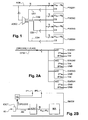
- FIGS 1 and 2A, 2B illustrate two conventional methods to achieve an extended memory plane, respectively with parallel type memories and serial memories.
- each memory has N address entries AI 0 -AI N-1 in parallel, connected to the N Leastweight address son of an address bus ADB.
- the address bus comprises N + 2 address wires, necessary for addressing the extended memory array whose size is here four times that of the memory planes integrated in the silicon chips.
- the selection of each memory within the extended memory array is made by means of a selection input CS ("Chip Select") provided on each silicon chip.
- the two most significant wires of the address bus ADB are applied to an address decoder ADEC which supplies four selection wires CS1, CS2, CS3, CS4, each selection wire being connected to the input CS of a memory.
- This example shows that the realization of a memory plan extended by means of integrated circuits with parallel inputs leads to a redhibitory reduction of the wires interconnection in order to be able to select individually the memories within the extended memory plane.
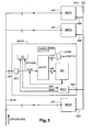
- Figure 2A relates more specifically to the field technique of the invention and represents an extended memory plane realized with four identical memories SMEM1, SMEM2, SMEM3, SMEM4 with serial input / output, or serial memories, whose structure is shown schematically in FIG. 2B.
- Each SMEM memory includes an IO serial input / output, a IOCT input / output circuit, a CPU, a counter address of N-bit ACNT and an addressable integrated memory array MA under N bits (Fig. 2B).
- the IOCT circuit is connected to IO serial input / output and transforms data received under series form in parallel data, and vice versa.
- Each IO serial input / output is connected to a DTW data wire (Fig. 2A) common to all memories, which conveys both commands, addresses and data in serial form.
- Each memory also includes two inputs IP1, IP0 whose electrical potential is adjusted so as to attribute to each memory an address of high weight determined.
- two inputs IP1, IPO of the memory SMEM1 are brought to a supply voltage Vcc for assigning the memory address weight "11"
- the inputs IP1, IP0 of the memory SMEM2 are respectively at voltage Vcc and at ground (GND) for assign to the memory the most significant address "10”
- the inputs IP1, IPO of the SMEM3 memory are grounded and the voltage Vcc to assign the memory the high-order address "01”
- the inputs IP1, IPO of the memory SMEM4 are brought to the mass to assign to the memory the high-order address "00".
- each memory within the extended memory array is made by sending to the memories commands of the type [OPCODE, I1, I0, AD] comprising an operation code OPCODE, two bits I1, I0 forming a most significant address and an address N-bit AD forming a low-order address, the high-order address forming an extended address with address AD.
- the central unit of each memory executes the OPCODE operation codes present in the received commands if the high-order address I1 I0 corresponds to the IP1 IPO high-order address assigned to the memory.
- the address counter ACNT applies to the memory plane MA the N address bits A N-1 -A 0 present in the command, whereas the central unit applies a read signal. to the memory plane.
- US 5,303,201 and US 5,895,480 disclose memories of the aforementioned type, in which the address counter (an address buffer in US 5,895,480) is an address counter extended (or extended address buffer) that can receive extended address instead of only receiving the weight address low.
- the operation of these memories is substantially identical to that of the memory described above, in that the most significant address received by the counter or address buffer is compared to the high-order address assigned to the memory, and in that a read command is not executed if the address weight present in an extended address is not identical to the most significant address assigned to the memory.
- the conventional method of obtaining a plan Extended memory consists of providing memories capable of "self-identify" upon receipt of an order including a extended address, and not to execute the command if the address weight in the extended address is not identical at the highest address assigned to the memory.
- a continuous reading of the extended memory plane requires all first sending to the first memory SMEM1 a command of continuous reading of its integrated memory plane, such a command including the operation code of the order, the weight address 1.1 strong of the SMEM1 memory, and the AD0 least significant address designating the memory area where continuous reading is to be initialized in the integrated memory plane.
- Some orders similar with appropriate identification bits shall then be sent to the other briefs, for a total of four commands to read the entire extended memory map.
- a general object of the present invention is to provide a method and a serial memory structure that allow to realize an extended memory plan having a character unitary, that is to say, behaving, seen from the outside, as a single memory comprising a large memory plane.
- a more particular object of the invention is to provide an extended memory plan having a unitary character with respect to regards the execution of a continuous reading command of the plan memory.
- a more particular object of the invention is to provide an extended memory plan having a unitary character with respect to concerning the execution of particular orders intended to read special registers that are usually provided for in the submissions series, for example status registers or registers Identification.
- a more particular object of the invention is to provide an extended memory plan having a unitary character with respect to the protection of the extended memory plane in reading and write when a memory is performing a write operation.
- At least one objective of the invention is achieved by the prediction of a memory on a silicon chip comprising a serial input / output, means for storing an address of weight assigned to memory within a memory plane addressable extended by means of an extended address including a low-weight address and a most significant address, a plan addressable built-in memory with the low-order address, at least one accessible reading register, means to provide a master memory signal having an active value or a inactive value, from the most significant address assigned to the memory, the memory signal master to the active value meaning that memory is master within the memory plane extended, the master memory signal to the inactive value meaning that the memory is slave within the memory plane extended, and a CPU to execute a command of reading the register and providing the contents of the register on the serial input / output of the memory, only if the memory is master memory within the extended memory plane.
- the memory comprises ways to memorize information on the size of the plan extended memory, and means for providing the memory signal master from the high-order address assigned to the memory and information on the size of the extended memory plane.
- the size information of the extended memory plane includes the number of bits that includes the most significant address present in an extended address.
- the master memory signal is raised to the active value if the assigned high-order address in memory is the highest strongest address assigned to the within the extended memory plane.
- the register is a register state comprising write protection bits of the plane extended memory.
- the register is a register identification data including identification data of the memory.
- the central unit is configured to execute a register write command whatever the value of the master memory signal.
- the means for providing a master memory signal include a decoding circuit receiving as input the information on the size of the memory array extended and the most significant address assigned to the memory.
- the memory comprises a Extended address counter for storing an extended address received on the serial input / output of the memory, means for compare the high-order address of the extended address with the highest-order address attributed to memory, and means to prevent the execution of a read or write command of the integrated memory map if the high-order address of the address extent is different from the most significant address assigned to the memory.
- the memory comprises a output buffer circuit to provide on the serial input / output the memory of the data read in the integrated memory plane, and a comparator for providing a circuit blocking signal output buffer if the high address of the extended address is different from the high-order address assigned to the memory.
- the memory comprises specific contacts to configure the weight address strongly attributed to memory, applying potential determined on each of the specific contacts.
- the present invention also relates to a method for realization of an extended memory map addressable by means of a extended address including a low-order address and a most significant address, the extended memory plane including a plurality of integrated serial memories on microchips of silicon, each memory comprising a serial input / output, a integrated addressable memory array with the low-order address, and at least one readable register after application to the memory of a read command of the register, the serial inputs / outputs of the memories being interconnected, the method comprising the steps of assigning each memory a high-order address within the extended memory plane, designate, in the extended memory plane, a single memory master and slave memories, and configure the memories so that only the master memory executes a read command of the registry, and that slave memories do not execute such ordered.
- the method comprises the steps of providing, in each memory, means for memorize the high-order address assigned to the memory, means for providing a master memory signal having a active value or an inactive value, from the address of weight attributed to the memory, the memory signal master to the active value meaning that the memory is master within the extended memory plane, the memory signal master to the value inactive meaning that memory is slave within the plane extended memory, and a CPU to execute a command reading the register and providing the contents of the register on the serial input / output of the memory, only if the memory is memory master within the extended memory plane.
- the method comprises the steps of providing, in each memory, means for memorize information on the size of the extended memory plane, and means for providing the master memory signal from of the high-order address assigned to the memory and of information on the size of the extended memory plane.
- the size information extended memory plan includes the number of high-order bits present in an extended address applied to the memory plane.
- each memory provides the master memory signal by means of a decoding circuit of information on the size of the extended memory plane and the most significant address assigned to the memory.
- a memory is memory master if she is assigned the highest weight address strong within the extended memory plane.
- the register is a register state comprising write protection bits of the plane extended memory.
- the register is a register identification data including identification data of the memory.
- a write command of the register is executed by all memories.
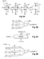
- FIG. 3 represents an extended memory plane comprising four memory memories MEM1, MEM2, MEM3, MEM4 according to the invention, integrated on silicon microchips.
- Each memory conventionally includes a serial IOP input / output contact (In / Out Pad), an IOCT input / output circuit ensuring conversion of data received in serial form into data parallel, and conversely, an addressable integrated memory map MA under N bits, and a wired logic UC CPU or microprocessor.
- Memories MEM1 to MEM4 have their respective IOP contacts connected to a common DTW data wire.
- This data thread belongs to a serial data bus that may include wires control like clock wires, power, mass ... who are not represented here.
- the address EAD is an extended address comprising an N + K number of address bits which is greater than the number N of address bits required for the addressing of the integrated memory plane of each memory, N + K being at least equal the number of address bits that the addressing of the extended memory array considered as a whole requires.
- the extended address EAD thus comprises N low order address bits A N-1 -A 0 forming a low dot address ADL intended to select a memory area in one of the integrated memory planes, generally a binary word, and K most significant address bits A N + K-1 , A N + K-2 , ... A N forming a most significant address ADH making it possible to designate one of the memories.
- K is equal to 2 because the extended memory plane comprises four serial memories.
- the commands thus comprise addresses of N + 2 bits.
- the address ADL comprises low-order address bits A N-1 -A 0 and the address ADH comprises 2 bits of high-order address A N + 1 , A N.
- Each memory includes an extended EACNT address counter of N + K bits, here N + 2 bits, a comparator COMP having twice K inputs (2 * K), here 4 inputs, and a storage means of a RADH reference high-order address assigned to the memory, which represents the address of the memory within the memory plane extended, specifically the address of the integrated memory map of the memory within the extended memory plane.
- This storage means is for example an indexing register IDXREG comprising K reference bits R K-1 , R K-2 , ... R 0 , here two bits R1, R0, representing the RADH address.
- IDXREG register of the memory MEM1 comprises the reference bits "00”
- the register IDXREG of the memory MEM2 comprises the reference bits "01”
- the register IDXREG of the memory MEM3 comprises the reference bits "10”
- the IDXREG register of the memory MEM4 comprises the reference bits "11".
- each memory When a command including an extended address is sent over the DTW data wire, each memory receives the command and applies the OPCODE operation code to its CPU, and stores the extended address EAD in its extended address counter EACNT.
- the comparator output provides an ADMATCH signal which is for example at 1 when the most significant bits of the address received range are identical to the assigned high-order address in memory, that is to say identical to the reference bits.
- the ADMATCH signal is used to prevent memories that are not not concerned with the extended address to execute the command received, whether it is a read command or a command (when the integrated memory schemes are accessible in writing).
- the non-execution of a write command is obtained classically by blocking the execution of the operation code by the CPU, with respect to the write commands.
- the non-execution of an order for reading is obtained by leaving the central unit of each memory execute the read operation while preventing the read data to be applied on the input / output contact IOP series.
- This method advantageously makes it possible to ensure Continuous reading of the extended memory plane, because it allows let the CPU of each memory read continuously its integrated memory map, and to provide the data read when the ADMATCH signal goes to 1.
- each memory includes an availability / occupation contact RBP (Ready / Busy Pad) and an RBCT circuit for managing the RBP contact.
- Contacts RBP memories are interconnected and are defaulted to a high potential, here a supply voltage Vcc, by through a high-value RPU high-value resistor.
- the RPU resistance is here external to the memories, but can also be internal to each memory, ie to be integrated on silicon chips.
- the RBCT circuit receives an IWIP signal (Internal Write In Progress) issued by the central unit, and provides the unit an EWIP (External Write In Progress) signal.
- the signal IWIP is set to 1 by the CPU during an operation writing of the integrated memory plane (deletion and / or programming).
- the RBCT circuit force the RBP contact to a low potential, for example the potential massive.
- the RBCT circuit sets the EWIP signal to 1 when it detects the low potential, here the mass potential, on the RBP contact, including when the IWIP signal is 0.
- the causes the EWIP signal to be 1 while the IWIP signal is 0 means that the mass potential on the RBP contact is imposed by another memory.
- the signal EWIP thus allows the unit central to know that a memory of the extended memory array is in perform a write operation in the memory plane which is proper to him.
- the CPU then refuses to execute a read or write command that can possibly be received on the IOP input / output contact, as long as the write course is not completed.
- the input / output circuit includes an input buffer INBUF having an input and a serial output, a register with INSEC shift with serial input and parallel output, an OUTBUF output buffer having an input and a serial output, and an OUTSREG shift register having a parallel input and a serial output.
- the buffer INBUF has its input connected to the contact IOP and its serial output connected to the serial input of the register INSREG, the output of which is connected to the data bus 5.
- the register OUTSREG has its input connected to data bus 5. Sa output is connected to the input of the OUTBUF buffer whose output is connected to the IOP contact.
- the memory plane MA comprises a matrix of memory cells FGTMTX, for example a matrix of gate transistors floating, a line and column decoder XYDEC, a circuit LATCHCT programming system including high voltage locks whose inputs are connected to the bus 5, and a read circuit SENSECT comprising reading amplifiers whose outputs are connected to the bus 5.
- FGTMTX for example a matrix of gate transistors floating
- XYDEC line and column decoder XYDEC
- circuit LATCHCT programming system including high voltage locks whose inputs are connected to the bus 5
- SENSECT comprising reading amplifiers whose outputs are connected to the bus 5.
- the special registers STREG and IDREG are accessible in read and write via the data bus 5.
- the IDREG register for example includes a unique ID ID of the silicon chip.
- the STREG status register includes example of the bits P0, P1, ... Pi write protection of fractions (parts) of the memory array, a protection WEN bit Write Enable, as well as a WP bit representative of the current value of the EWIP signal, and so general data useful for the management of a known memory of the skilled person.
- the central unit controls the various elements of the memory, the control links between the CPU and these various elements being represented schematically by a line dotted.
- the central unit controls the various registers for reading and / or writing, reading control and write the memory plane MA and its constituent elements, controls the EACNT Extended Address Counter for charging extended address and / or for incrementing or decrementation of the counter, when executing commands from continuous reading, controls the loading of the registers to shift, etc.
- the CKGEN clock generator provides a clock signal CK1 which is a submultiple of the signal CK0.
- the signal CK0 is a bit clock signal while the signal CK1 is a signal word clock, whose frequency is equal to the frequency of the clock signal CK0 divided by the number of bits that include the binary words present in the memory plane.
- the clock signal CK1 cadence the operations involving words binaries, in particular reading or writing the memory plane, incrementing or decrementing the address counter EACNt, loading a binary word in the OUTSREG register or reading of a binary word in the INSREG register, etc.
- clock signal CK0 cadence the operations related to the transmission or reception of bits in serial form, in particular the shift of bits in the shift registers OUTSREG, INSREG and the timing of buffers OUTBUF, INBUF.
- the OPCODE operation codes and the EAD extended addresses received in serial form on the IOP contact are transformed by the register INSEC into parallel data applied on the bus 5, and are respectively applied to an input of the central unit and an input of the counter.
- extended address EACNT When an EAD address has been registered in the EACNT address counter, it provides the first N address bits N-1 -A 0 (ADL address) to the XYDEC decoder, and provides the address bits of strong weight A N + 2 , A N + 1 , A N (ADH address) at first inputs of comparator COMP.
- the indexing register IDXREG here comprises three reference bits R2, R1, R0 which form the RADH reference high-order address assigned to the memory within the extended memory plane.
- An extended address thus comprises, at most, 3 bits of most significant address A N + 2 , A N + 1 , A N.
- Bits R2, R1, R0 are applied on second inputs COMP comparator whose output provides the signal ADMATCH described above.
- the ADMATCH signal is applied to the central unit for block the execution of write commands.
- ADMATCH signal is also applied to an input of a gate 10 of type NO OR two inputs, whose output provides a SHZ signal (Set High Z).
- the SHZ signal is applied to a control input of the output buffer OUTBUF via the circuit SYNCCT synchronization.
- OUTBUF output buffer is a buffer three states that can have an output state of 0 (mass), 1 (Vcc) or high impedance (HZ). When the signal SHZ is at 1, the OUTBUF buffer puts its output at high impedance.
- the circuit of SYNCCT synchronization is usually transparent to the SHZ signal, except in a particular case described below.
- the signal ADMATCH goes to 0 and the signal SHZ goes to 1, which toggles OUTBUF buffer output in the high impedance state.
- the data applied on the input buffer series are no longer transmitted to the contact IOP input / output, which makes it possible not to execute a read command.
- the central unit meanwhile, is configured to execute the read command, in accordance with the method according to the invention for not executing a command of reading, according to which the data are read but blocked in exit.
- the SYNCCT circuit becomes non-transparent vis-à-vis the SHZ signal when a signal LOAD loading a binary word is applied to the OUTSREG shift register by the central processing unit. From this moment, the SYNCCT circuit counts a number of CK0 clock cycles corresponding to the number of bits present in a binary word, ie a clock cycle CK1, and becomes again transparent when the transmission cycle of the binary word is completed. So, if the SHZ signal goes to 1 then a word binary is being sent bit by bit on the contact of IOP output, blocking (high impedance setting) of the buffer exit occurs only after the full word has been sent.
- the RBCT circuit comprises a switch transistor T1, here of the NMOS type, an OR type gate 20 and an inverting gate 21.
- the drain and source terminals of transistor T1 are connected respectively at the RBP contact and at ground, while the gate of the transistor is driven by the IWIP signal provided by the unit Central.
- the gate 21 is connected as input to the RBP contact.
- the gate 20 receives on one input the signal IWIP, on another input the output of the gate 21, and its output provides the signal EWIP.
- the IWIP signal is set when the central unit performs an erasure operation and / or programming in the memory plane.
- the RBP contact which is biased at the voltage Vcc by the resistor RPU described previously, is then forced to 0 (ground) by the transistor T1.
- the memory includes a CNFREG configuration register and a CNFDEC configuration decoder.
- the size of the extended memory array is thus equal to 2 K times the size of the integrated memory array MA, ie a number of memory points (binary words) equal to 2 K * 2 N or 2 N + K.
- the output of the CNFREG register is applied to the decoder of CNFDEC configuration which provides, from K, three flags F2, F1, F0 indicating the number of most significant address bits that includes the extended address of the extended memory plane.
- flags F2, F1, F0 can also be directly recorded in the CNFREG register, memorization of the parameter K in binary form being provided here to reduce the size of the CNFREG register.
- the relation between the number K and the flags F2, F1, F0 is described in Table 1 below.
- the decimal value of K is described in the first column of the table.
- There binary value of K (bits K1, K0) is described by the second column.
- Size extended memory plane is described by the third column of board.
- the fourth, fifth and sixth columns describe respectively the values of the flags F2, F1, F0 for each value of K.
- the seventh column mentions the address bits of weight (address bits beyond the first N bits) that includes the extended address, for each value of K.
- the last column describes the maximum value MSBmax of the weight address strong in the extended memory plane, for each value of K.
- the flag F0 is at 0 only when K is equal to 0.
- the fact that the flag F0 is 0 means that the memory is not integrated in a memory array extended, and that there is no high-order address.
- the memory then operates in "classical" mode, that is to say by executing all the commands without its operation being dependent on the comparison of the most significant address bits and the reference bits R2, R1, R0.
- the flag F0 is applied to the input of an inverting gate 11 whose output provides an ADMATCH signal.
- the signal ADMATCH ' is applied on the second entry of the gate 10.
- extended address counter and / or comparator have a variable configuration that is K.'s function
- Figures 5A and 5B represent respectively a first EACNT1 embodiment of the extended address counter and a first embodiment COMP1 of the comparator.
- the counter of address includes a variable number of counting cells active, which is a function of K, while the comparator includes a number of comparison entries that is fixed and equal at Kmax.
- the EACNT1 address counter includes a base count block BCNT comprising N cells counting of 1 bit each (not shown) and three cells additional counting C1, C2, C3 of 1 bit each, arranged outside the base count block.
- the various cells counting are clocked by the clock signal CK1.
- the basic count block BCNT receives as input the address bits A N-1 -A 0 , ie the address ADL, and supplies address bits A N-1 '-A 0 '.
- the address bits A N-1 '-A 0 ' are equal to the address bits received at the input in the case of a fixed address read or write command, or form an incremented or decremented address at the rate of the clock signal CK1 in the case of a continuous read command.
- the count block BCNT provides a sum carry-over bit C (Carry) when it reaches the overflow value (all address bits at 1) and when it returns to 0.
- the counting cells C1, C2, C3 each comprise an input In to receive a high-order address bit, respectively A N , A N + 1 , A N + 2 , together forming the address ADH, and an output providing address bits A N ', A N + 1 ', A N + 2 ', respectively.
- Each counting cell C1, C2, C3 comprises a CIN input to receive the C bit of the previous rank and a COUT output to supply the C bit of the next rank.
- the input CIN of the cell C1 receives the bit C supplied by the block BCNT via an AND gate whose other input receives the flag F0.
- the input CIN of the cell C2 receives the bit C supplied by the cell C1 via an AND gate whose other input receives the F1 flag.
- the input CIN of the cell C3 receives the bit C supplied by the cell C2 via an AND gate whose other input receives the flag F2.
- the flags F0 to F2 are all 0, the three cells are disconnected and the address counter includes only the base counter BCNT, which is equivalent to an address counter of a conventional memory.
- the memory operates in this case in "conventional" mode: the signal ADMATCH 'is at 1 and forces at 0 the signal SHZ, as described above.
- the comparator COMP1 shown in FIG. 5B comprises doors 30, 31, 32 of the EXCLUSIVE OR type and a gate 33 of the NON OR type.
- the gate 30 receives as input the reference bit R0 and the most significant address bit A N '.
- Gate 31 receives as input the reference bit R1 and the most significant address bit A N + 1 '.
- the gate 32 receives as input the reference bit R2 and the most significant address bit A N + 2 '.
- the gate 33 has three inputs respectively connected to the outputs of the doors 30, 31, 32, and provides the signal ADMATCH.
- FIGS. 6A and 6B respectively represent a second EACNT2 embodiment of the extended address counter and a second COMP2 embodiment of the comparator.
- the EACNT2 address counter includes a invariable number N + Kmax of active counting cells.
- the EACNT2 counter is the equivalent of the EACNT1 counter in which the AND gates for filtering the sum carry bits C are deleted and replaced by direct connections.
- the comparator COMP2 has the same doors as the comparator COMP1 described above, designated by the same references. It further comprises doors 34, 35, 36 of type AND.
- the gate 34 receives as input the output of the gate 30 and the flag F0. Its output is applied to the first input of the door 33.
- the door 35 receives as input the output of the door 31 and the F1 flag. Its output is applied on the second input of the door 33.
- the door 36 receives as input the output of the door 32 and the flag F2. Its output is applied to the third entrance to the door 33. Thus, the entrances of the comparator are inhibited by the flags F0, F1, F2 when these are at 0.
- the entries of the comparator corresponding to the inputs of the gate 30 are inhibited when the flag F0 is 0.
- the entries of the corresponding to the inputs of the gates 30, 31 are inhibited when the flags F0, F1 are at 0.
- all comparator inputs are inhibited when all flags F0, F1, F2 are 0, the ADMATCH signal is then forced to 1.
- This embodiment of the comparator makes it possible to remove the doors 10, 11, the signal ADMATCH can be directly applied to the SYNCCT circuit.
- serial memory a programmable configuration allowing it to work as a classic serial memory, or to be integrated into a extended memory map whose size is 2 times, 4 times or 8 times the size of his own memory plane.
- the programming of the CNFREG configuration register is preferably made by software, by means of a specific command the CPU executes. This programming can be when all the memories are interconnected, because the K value is the same for all memories.
- the programming of the indexing register IDXREG must, however, be assured before the interconnection of the memories, because each memory must receive an individual high-value address and the execution of an individual command to write the register IDXREG can only be considered as one of the most significant is not registered.
- the IDXREG register can be programmed during the manufacture of silicon chips, which are then classified in batches, each batch corresponding to a most significant address. This solution will however, against the flexibility sought.
- a more advantageous solution consists in providing electrical contacts, here three contacts IDXP0, IDXP1, IDXP2 linked to corresponding IDXREG register entries respectively to the reference bits R0, R1, R2.
- Contacts IDXP0, IDXP1, IDXP2 are connected to the ground by a resistor high-value RPD low-cut, individual or collective.
- each contact IDXP0, IDXP1, IDXP2 is connected to the voltage Vcc for program to 1 of the corresponding reference bit, or is left disconnected to program the corresponding reference bit to 0.
- Table 2 below describes the various high-order addresses that can be loaded in the register IDXREG as a function of the value of K (K1 K0) loaded into the register CNFREG.
- the goal of the invention is here to ensure that when a control of reading of such a register is applied to a set of memories, a single memory processes the command and provides on the serial bus the contents of the special register, in order to avoid collisions of answers.
- the memory includes a master memory decoder MSTDEC which provides a MASTER signal (Fig. 6).
- MASTER signal When MASTER signal is at 1, the memory is considered as master's memory within of the extended memory map while the other memories are considered as slaves.
- a single memory that can be a master within the same extended memory plane, the MASTER signal must be at 1 for a single memory.
- a solution others is to confer the status of master memory to the one who receives in the register IDXREG a most significant address which is the highest high order address of the extended memory plane.
- the decoder MSTDEC receives as input the reference bits R0, R1, R2 and the bits K1, K0 forming the number K.
- the central unit UC is configured to execute a read command of one of the special registers STREG, IDREG only if the signal MASTER is at 1.
- the register is then transferred to the IOP output of the memory via the internal data bus 5 and the IOCT circuit.
- the extended memory plane has a unitary character with regard to the reading of the special registers since it is always the master memory that responds to the reading commands. In other words, everything happens as if the extended memory plane had only one copy of each of the special registers, those of the slave memories never being read and remaining inaccessible from the outside.
- K decimal
- CNFREG K1 K0
- IDXREG R2 R1 R0
- the protection bits in write P0 to Pi are assigned to the write protection of fractions of the extended memory array rather than the protection of fractions of the integrated memory map of the memory in which they are saved. These bits therefore concern each of the memories, in particular those which form part, as the case may be, of the fraction of the extended memory array to be write protected. Also, the bit WEN is used as a collective bit assigned to protection write procedure of the extended memory map, and not the write protection of a specific memory.
- write commands special registers are executed by all memories, masters or slaves. Special registers therefore contain exactly the same value in each of the memories of the extended memory plane and each form the equivalent a single collective register.
- a variant of this aspect of the invention consists of confer the status of memory master to the memory having the most low high-order address, ie all reference bits at 0. In this case, it is not necessary for the memory to compare its bits of reference to the bits K0, K1 of the number K to know if it is memory master or not.
- Such a command includes an extended address EAD0 of the beginning of reading, ie a N + K bit address:
- the respective CPUs of the memories increment or continuously decrement and simultaneously their counters extended address, and each provides the requested data when the most significant bits of the extended address counter become equal to the reference bits present in the register indexing.
- the memories are automatically relayed for provide on the serial bus the contents of their memory plans respective components, which corresponds, from the outside, to a single memory with a large integrated memory array size that would perform a continuous read operation of his memory map.
- FIGS. 7A to 7J illustrate the execution of a continuous read command of the extended memory plane represented in FIG. 3, formed by the memories MEM1 to MEM4.
- FIGS. 7A, 7C, 7E, 7G represent count values CNTVAL1, CNTVAL2, CNTVAL3, CNTVAL4 formed by the first N bits of the extended address counter of the memories MEM1, MEM2, MEM3, MEM4, respectively, or the ADL addresses.
- FIGS. 7A, 7C, 7E, 7G also represent the values of the signals ADMATCH1, ADMATCH2, ADMATCH3, ADMATCH4 at the output of the respective comparators of the memories MEM1, MEM2, MEM3, MEM4.
- FIG. 7B, 7D, 7F, 7H represent the data DTREAD1, DTREAD2, DTREAD3, DTREAD4 read in the integrated memory banks MEM1, MEM2, MEM3, MEM4, respectively.
- the count values of low weight CNTVAL1, CNTVAL2, CNTVAL3, CNTVALA perform several counting cycles, each time going back to zero (Fig. 7A, 7C, 7E, 7G) while the weight count value strength increases by one unit each cycle.
- central units of the memories read all of their plans respective memory, but these data are not output than when the ADMATCH signal is at 1. So the data provided during the first cycle of counting are those are read by memory MEM1, and extend from the first word binary DT10 to the last binary word DT1x present in the memory MEM1.
- the data provided during the second cycle of count are those read by memory MEM2 and extend from the first binary word DT20 to the last word binary DT2x present in the memory MEM2.
- the data provided during the third round of counting are those are read by memory MEM3 and extend from the first word binary DT30 to the last binary word DT3x present in the memory MEM3.
- the data provided are those read by the memory MEM4, and extend from the first binary word DT40 to the last bit word DT4x present in the memory MEM4. The judgment of However, the reading process can occur at any time, and is usually triggered by ceasing to apply the signal clock CK0 to memories.
- the non-execution of a continuous read command by performing a reading of the integrated memory plane while blocking the data at the memory output presents a determining advantage in relation to a method that would consist of not to read the memory map.
- This other method would require the provision of a complex decoder bearing on all the address bits of the counter to anticipate the moment where data will have to be provided, in order to initialize the reading of the memory map in a timely manner during the execution of a continuous read command during which the counter extended address is continually incremented or decremented.
- a memory according to the invention is susceptible of various variants and modes of realization. Various combinations of the means of the invention may be provided, some means may not be artwork.
- the implementation of the contact of availability / occupancy RBP and EWIP signal is justified only if the integrated memory map of each memory is accessible to the times in reading and writing (for example a memory map of Flash type or EEPROM).
- the meter forecast configurable address and / or configurable comparator justifies that if one wishes to provide a configurable memory, intended to be incorporated into an extended memory plane whose size is not predetermined.
- the signal forecast memory is justifiable only if one wishes to foresee a extended memory map capable of responding to a read command special registers.
- the invention also applies to the production of a composite extended memory plane.
- N and K are different in each memory but the sum of N and K is constant and equal to the number of bits that the address extended extent of the composite extended memory plane.
Landscapes
- Engineering & Computer Science (AREA)
- Microelectronics & Electronic Packaging (AREA)
- Read Only Memory (AREA)
- Dram (AREA)
Abstract
Description
- la figure 1 précédemment décrite représente un plan mémoire étendu comprenant des mémoires de type parallèle,
- les figures 2A, 2B précédemment décrites représentent respectivement un plan mémoire étendu comprenant des mémoires série classiques et la structure de ces mémoires série,
- la figure 3 représente un plan mémoire étendu comprenant des mémoires série selon l'invention, et représente schématiquement la structure de l'une de ces mémoires série,
- la figure 4 représente sous forme de blocs un exemple de réalisation d'une mémoire série selon l'invention,
- la figure 5A représente un premier exemple de réalisation d'un compteur d'adresse étendue représenté sous forme de bloc en figure 4,
- la figure 5B représente un premier exemple de réalisation d'un comparateur représenté sous forme de bloc en figure 4,
- la figure 6A représente un second exemple de réalisation du compteur d'adresse étendue représenté sous forme de bloc en figure 4,
- la figure 6B représente un second exemple de réalisation du comparateur représenté sous forme de bloc en figure 4,
- les figures 7A à 7J sont des chronogrammes représentant des signaux de comptage et des signaux de données et illustrant le fonctionnement d'un plan mémoire étendu selon l'invention en réponse à une commande de lecture continue.
ou
- le contact IOP formant l'entrée/sortie série de la mémoire,
- le contact de disponibilité/occupation RBP,
- le circuit d'entrée/sortie IOCT,
- le circuit RBCT de gestion du contact RBP,
- l'unité centrale UC,
- le compteur d'adresse étendue EACNT,
- le plan mémoire MA adressable sous N bits,
- le registre d'indexation IDXREG, et
- le comparateur COMP.
- un bus de données interne 5 de type parallèle,
- un contact de masse GNDP,
- un contact d'horloge CKP recevant un signal d'horloge CK0,
- un circuit d'horloge CKGEN,
- un circuit de synchronisation SYNCCT, et
- deux registres spéciaux, ici un registre d'état STREG (Statuts Register) et un registre d'identification IDREG.
| K(décimal) | K1 K0 | 2K*2N | F2 | F1 | F0 | MSB | MSBmax |
| 0 | 00 | 2N | 0 | 0 | 0 | - | - |
| 1 | 01 | 2*2N | 0 | 0 | 1 | AN | 1 |
| 2 | 10 | 4*2N | 0 | 1 | 1 | AN+1 AN | 11 |
| 3 | 11 | 8*2N | 1 | 1 | 1 | AN+2 AN+1 AN | 111 |
| CNFREG (K1 K0) | IDXREG (R2 R1 R0) |
| 00 | 000 |
| 01 | 000 ou 001 |
| 10 | de 000 à 011 |
| 11 | de 000 à 111 |
| K(décimal) | CNFREG (K1 K0) | IDXREG (R2 R1 R0) | MASTER |
| 0 | 00 | 000 | 1 |
| 1 | 01 | 001 | 1 |
| 1 | 01 | 000 | 0 |
| 2 | 10 | 011 | 1 |
| 2 | 10 | de 000 à 010 | 0 |
| 3 | 11 | 111 | 1 |
| 3 | 11 | de 000à 110 | 0 |
Claims (20)
- Mémoire (MEM) sur microplaquette de silicium, comprenant :au moins un registre (STREG, IDREG) accessible en lecture,une entrée/sortie série,des moyens (IDXREG) pour mémoriser une adresse de poids fort (RADH) attribuée à la mémoire au sein d'un plan mémoire étendu adressable au moyen d'une adresse étendue (EAD) comprenant une adresse de poids faible (ADL) et une adresse de poids fort (ADH),un plan mémoire intégré (MA) adressable avec l'adresse de poids faible (ADL), et
caractérisée en ce qu'elle comprend :des moyens (MSTDEC) pour fournir un signal de mémoire maítre (MASTER) présentant une valeur active ou une valeur inactive, à partir de l'adresse de poids fort (RADH) attribuée à la mémoire, le signal de mémoire maítre à la valeur active signifiant que la mémoire est maítre au sein du plan mémoire étendu, le signal de mémoire maítre à la valeur inactive signifiant que la mémoire est esclave au sein du plan mémoire étendu, etune unité centrale (UC) pour exécuter une commande de lecture du registre (STREG, IDREG) et de fourniture du contenu du registre sur l'entrée/sortie série de la mémoire, uniquement si la mémoire est mémoire maítre au sein du plan mémoire étendu. - Mémoire selon la revendication 1, comprenant :des moyens (CNFREG) pour mémoriser une information (K1, K0) sur la taille du plan mémoire étendu, etdes moyens (MSTDEC) pour fournir le signal de mémoire maítre à partir de l'adresse de poids fort (RADH) attribuée à la mémoire et de l'information (K1, K0) sur la taille du plan mémoire étendu.
- Mémoire selon la revendication 2, dans laquelle l'information (K1, K0) sur la taille du plan mémoire étendu comprend le nombre (K) de bits que comprend l'adresse de poids fort (ADH) présente dans une adresse étendue (EAD).
- Mémoire selon l'une des revendications 2 et 3, dans laquelle le signal de mémoire maítre est porté à la valeur active si l'adresse de poids fort (RADH) attribuée à la mémoire est la plus forte adresse de poids fort (RADH) attribuée au sein du plan mémoire étendu.
- Mémoire selon l'une des revendications 1 à 4, dans laquelle le registre est un registre d'état (STREG) comprenant des bits de protection en écriture du plan mémoire étendu.
- Mémoire selon l'une des revendications 1 à 5, dans laquelle le registre est un registre d'identification (IDREG) comprenant une donnée d'identification de la mémoire.
- Mémoire selon l'une des revendications 1 à 6, dans laquelle l'unité centrale est configurée pour exécuter une commande d'écriture du registre (STREG, IDREG) quelle que soit la valeur du signal de mémoire maítre.
- Mémoire selon l'une des revendications 2 à 4, dans laquelle les moyens pour fournir un signal de mémoire maítre comprennent un circuit de décodage (MSTDEC) recevant en entrée l'information (K1, K0) sur la taille du plan mémoire étendu et l'adresse de poids fort (RADH) attribuée à la mémoire.
- Mémoire selon l'une des revendications 1 à 8, comprenant :un compteur d'adresse étendue (EACNT) pour mémoriser une adresse étendue (EAD) reçue sur l'entrée/sortie série de la mémoire,des moyens (COMP) pour comparer l'adresse de poids fort (ADH) de l'adresse étendue avec l'adresse de poids fort (RADH) attribuée à la mémoire, etdes moyens (COMP, ADMATCH, SHZ, OUTBUF) pour empêcher l'exécution d'une commande de lecture ou d'écriture du plan mémoire intégré (MA) si l'adresse de poids fort (ADH) de l'adresse étendue est différente de l'adresse de poids fort (RADH) attribuée à la mémoire.
- Mémoire selon la revendication 9, comprenantun circuit tampon de sortie (OUTBUF) pour fournir sur l'entrée/sortie série de la mémoire des données lues dans le plan mémoire intégré (MA), etun comparateur (COMP) pour fournir un signal de blocage (ADMATCH, SHZ) du circuit tampon de sortie (OUTBUF) si l'adresse de poids fort (ADH) de l'adresse étendue est différente de l'adresse de poids fort (RADH) attribuée à la mémoire.
- Mémoire selon l'une des revendications 1 à 11, comprenant des contacts spécifiques (IDXP0-IDXP2) permettant de configurer l'adresse de poids fort (RADH) attribuée à la mémoire, en appliquant des potentiels électriques déterminés sur chacun des contacts spécifiques.
- Procédé pour la réalisation d'un plan mémoire étendu adressable au moyen d'une adresse étendue (EAD) comprenant une adresse de poids faible (ADL) et une adresse de poids fort (ADH), le plan mémoire étendu comprenant une pluralité de mémoires série intégrées sur microplaquettes de silicium, chaque mémoire comprenant une entrée/sortie série, un plan mémoire intégré (MA) adressable avec l'adresse de poids faible (ADL), et au moins un registre (STREG, IDREG) accessible en lecture après application à la mémoire d'une commande de lecture du registre, les entrées/sorties série des mémoires étant interconnectées, procédé comprenant les étapes consistant à :attribuer à chaque mémoire une adresse de poids fort (RADH) au sein du plan mémoire étendu,désigner, dans le plan mémoire étendu, une seule mémoire maítre et des mémoires esclaves, etconfigurer les mémoires de manière que seule la mémoire maítre exécute une commande de lecture du registre (STREG, IDREG), et que les mémoires esclaves n'exécutent pas une telle commande.
- Procédé selon la revendication 12, comprenant les étapes consistant à prévoir, dans chaque mémoire :des moyens (IDXREG) pour mémoriser l'adresse de poids fort (RADH) attribuée à la mémoire,des moyens (MSTDEC) pour fournir un signal de mémoire maítre présentant une valeur active ou une valeur inactive, à partir de l'adresse de poids fort (RADH) attribuée à la mémoire, le signal de mémoire maítre à la valeur active signifiant que la mémoire est maítre au sein du plan mémoire étendu, le signal de mémoire maítre à la valeur inactive signifiant que la mémoire est esclave au sein du plan mémoire étendu, etune unité centrale (UC) pour exécuter une commande de lecture du registre (STREG, IDREG) et de fourniture du contenu du registre sur l'entrée/sortie série de la mémoire, uniquement si la mémoire est mémoire maítre au sein du plan mémoire étendu.
- Procédé selon la revendication 13, comprenant les étapes consistant à prévoir, dans chaque mémoire :des moyens (CNFREG) pour mémoriser une information (K1, K0) sur la taille du plan mémoire étendu, etdes moyens (MSTDEC) pour fournir le signal de mémoire maítre à partir de l'adresse de poids fort (RADH) attribuée à la mémoire et de l'information (K1, K0) sur la taille du plan mémoire étendu.
- Procédé selon la revendication 14, dans lequel l'information (K1, K0) sur la taille du plan mémoire étendu comprend le nombre de bits de poids fort présents dans une adresse étendue (EAD) appliquée au plan mémoire.
- Procédé selon l'une des revendications 14 et 15, dans lequel chaque mémoire fournit le signal de mémoire maítre au moyen d'un circuit (MSTDEC) de décodage de l'information (K1, K0) sur la taille du plan mémoire étendu et de l'adresse de poids fort (RADH) attribuée à la mémoire.
- Procédé selon l'une des revendications 12 à 16, dans lequel une mémoire est mémoire maítre si elle se voit attribuer la plus forte adresse de poids fort (RADH) au sein du plan mémoire étendu.
- Procédé selon l'une des revendications 12 à 17, dans lequel le registre est un registre d'état (STREG) comprenant des bits de protection en écriture du plan mémoire étendu.
- Procédé selon l'une des revendications 12 à 18, dans lequel le registre est un registre d'identification (IDREG) comprenant une donnée d'identification de la mémoire.
- Procédé selon l'une des revendications 12 à 19, dans lequel une commande d'écriture du registre (STREG, IDREG) est exécutée par toutes les mémoires.
Applications Claiming Priority (6)
| Application Number | Priority Date | Filing Date | Title |
|---|---|---|---|
| FR0314621 | 2003-12-12 | ||
| FR0314628 | 2003-12-12 | ||
| FR0314621A FR2863766A1 (fr) | 2003-12-12 | 2003-12-12 | Memoire serie comprenant des moyens d'integration dans un plan memoire etendu |
| FR0314628A FR2863765A1 (fr) | 2003-12-12 | 2003-12-12 | Procede de realisation d'un plan memoire etendu au moyen d'une pluralite de memoires serie |
| FR0314622 | 2003-12-12 | ||
| FR0314622A FR2863764A1 (fr) | 2003-12-12 | 2003-12-12 | Memoire serie comprenant des moyens de protection d'un plan memoire entendu pendant une operation d'ecriture |
Publications (2)
| Publication Number | Publication Date |
|---|---|
| EP1542233A1 true EP1542233A1 (fr) | 2005-06-15 |
| EP1542233B1 EP1542233B1 (fr) | 2007-05-30 |
Family
ID=34527436
Family Applications (3)
| Application Number | Title | Priority Date | Filing Date |
|---|---|---|---|
| EP04029017A Withdrawn EP1542234A3 (fr) | 2003-12-12 | 2004-12-08 | Procédé de réalisation d'un plan mémoire étendu au moyen d'une pluralité de mémoires série |
| EP04029018A Expired - Lifetime EP1542130B1 (fr) | 2003-12-12 | 2004-12-08 | Mémoire série comprenant des moyens d'intégration dans un plan mémoire étendu |
| EP04029016A Expired - Lifetime EP1542233B1 (fr) | 2003-12-12 | 2004-12-08 | Mémoire série comprenant des moyens de protection d'un plan mémoire étendu pendant une opération d'écriture |
Family Applications Before (2)
| Application Number | Title | Priority Date | Filing Date |
|---|---|---|---|
| EP04029017A Withdrawn EP1542234A3 (fr) | 2003-12-12 | 2004-12-08 | Procédé de réalisation d'un plan mémoire étendu au moyen d'une pluralité de mémoires série |
| EP04029018A Expired - Lifetime EP1542130B1 (fr) | 2003-12-12 | 2004-12-08 | Mémoire série comprenant des moyens d'intégration dans un plan mémoire étendu |
Country Status (3)
| Country | Link |
|---|---|
| US (3) | US7330381B2 (fr) |
| EP (3) | EP1542234A3 (fr) |
| DE (2) | DE602004005806T2 (fr) |
Cited By (1)
| Publication number | Priority date | Publication date | Assignee | Title |
|---|---|---|---|---|
| CN115705887A (zh) * | 2021-08-12 | 2023-02-17 | 美光科技公司 | 存储器操作完成标记 |
Families Citing this family (6)
| Publication number | Priority date | Publication date | Assignee | Title |
|---|---|---|---|---|
| EP2382637B1 (fr) * | 2008-12-30 | 2016-01-06 | Micron Technology, Inc. | Capacité d'adressage améliorée pour mémoire rémanente série |
| US8898439B2 (en) * | 2009-07-17 | 2014-11-25 | Macronix International Co., Ltd. | Serial flash memory and address transmission method thereof |
| US8677100B2 (en) * | 2009-07-17 | 2014-03-18 | Macronix International Co., Ltd. | Serial memory interface for extended address space |
| KR101903095B1 (ko) * | 2011-11-21 | 2018-10-02 | 삼성전자주식회사 | 불휘발성 메모리 장치 및 불휘발성 메모리 장치를 제어하는 컨트롤러의 동작 방법 |
| US11494317B1 (en) | 2020-12-29 | 2022-11-08 | Waymo Llc | Memory validation |
| FR3160478B1 (fr) * | 2024-03-20 | 2026-02-13 | Safran Electronics & Defense | Système de traitement d’entrées-sorties pour des architectures numériques séries et procédé associé |
Citations (2)
| Publication number | Priority date | Publication date | Assignee | Title |
|---|---|---|---|---|
| EP0028916A2 (fr) * | 1979-11-12 | 1981-05-20 | Fujitsu Limited | Dispositif de mémoire à semi-conducteur |
| US5303201A (en) * | 1992-03-30 | 1994-04-12 | Kabushiki Kaisha Toshiba | Semiconductor memory and semiconductor memory board using the same |
Family Cites Families (25)
| Publication number | Priority date | Publication date | Assignee | Title |
|---|---|---|---|---|
| US4128883A (en) * | 1977-09-30 | 1978-12-05 | Ncr Corporation | Shared busy means in a common bus environment |
| US4665506A (en) * | 1983-01-03 | 1987-05-12 | Texas Instruments Incorporated | Memory system with write protection |
| US4931997A (en) * | 1987-03-16 | 1990-06-05 | Hitachi Ltd. | Semiconductor memory having storage buffer to save control data during bulk erase |
| US4908789A (en) * | 1987-04-01 | 1990-03-13 | International Business Machines Corporation | Method and system for automatically assigning memory modules of different predetermined capacities to contiguous segments of a linear address range |
| US4905137A (en) * | 1987-12-18 | 1990-02-27 | North American Philips Corporation Signetics Division | Data bus control of ROM units in information processing system |
| US5357621A (en) * | 1990-09-04 | 1994-10-18 | Hewlett-Packard Company | Serial architecture for memory module control |
| US5430859A (en) * | 1991-07-26 | 1995-07-04 | Sundisk Corporation | Solid state memory system including plural memory chips and a serialized bus |
| US5428566A (en) * | 1993-10-27 | 1995-06-27 | Intel Corporation | Nonvolatile memory card with ready and busy indication and pin count minimization |
| JP3059349B2 (ja) * | 1994-12-19 | 2000-07-04 | シャープ株式会社 | Icカード、及びフラッシュメモリの並列処理方法 |
| US5737748A (en) * | 1995-03-15 | 1998-04-07 | Texas Instruments Incorporated | Microprocessor unit having a first level write-through cache memory and a smaller second-level write-back cache memory |
| KR0145222B1 (ko) * | 1995-05-20 | 1998-08-17 | 김광호 | 반도체 메모리장치의 메모리 셀 테스트 제어회로 및 방법 |
| US5592488A (en) * | 1995-06-07 | 1997-01-07 | Micron Technology, Inc. | Method and apparatus for pipelined multiplexing employing analog delays for a multiport interface |
| US5895480A (en) * | 1995-10-10 | 1999-04-20 | Holtek Microelectronics, Inc. | Method of and means for accessing an address by respectively substracting base addresses of memory integrated circuits from an access address |
| US5857214A (en) * | 1995-12-18 | 1999-01-05 | Advanced Micro Devices, Inc. | Microprocessor with a fixed cache size selected from a predesigned set of sizes |
| JP3850067B2 (ja) * | 1996-04-24 | 2006-11-29 | 株式会社ルネサステクノロジ | メモリシステムおよびそれに用いられる半導体記憶装置 |
| US5937423A (en) * | 1996-12-26 | 1999-08-10 | Intel Corporation | Register interface for flash EEPROM memory arrays |
| US6279069B1 (en) * | 1996-12-26 | 2001-08-21 | Intel Corporation | Interface for flash EEPROM memory arrays |
| US6175891B1 (en) * | 1997-04-23 | 2001-01-16 | Micron Technology, Inc. | System and method for assigning addresses to memory devices |
| US6442644B1 (en) * | 1997-08-11 | 2002-08-27 | Advanced Memory International, Inc. | Memory system having synchronous-link DRAM (SLDRAM) devices and controller |
| US6247084B1 (en) * | 1997-10-08 | 2001-06-12 | Lsi Logic Corporation | Integrated circuit with unified memory system and dual bus architecture |
| US6377502B1 (en) * | 1999-05-10 | 2002-04-23 | Kabushiki Kaisha Toshiba | Semiconductor device that enables simultaneous read and write/erase operation |
| JP2001167586A (ja) * | 1999-12-08 | 2001-06-22 | Toshiba Corp | 不揮発性半導体メモリ装置 |
| TW561491B (en) * | 2001-06-29 | 2003-11-11 | Toshiba Corp | Semiconductor memory device |
| KR100437467B1 (ko) * | 2002-07-03 | 2004-06-23 | 삼성전자주식회사 | 연속 버스트 읽기 동작 모드를 갖는 멀티 칩 시스템 |
| US20060014125A1 (en) * | 2004-07-14 | 2006-01-19 | St Clair John Q | Walking through walls training system |
-
2004
- 2004-12-08 EP EP04029017A patent/EP1542234A3/fr not_active Withdrawn
- 2004-12-08 EP EP04029018A patent/EP1542130B1/fr not_active Expired - Lifetime
- 2004-12-08 EP EP04029016A patent/EP1542233B1/fr not_active Expired - Lifetime
- 2004-12-08 DE DE602004005806T patent/DE602004005806T2/de not_active Expired - Lifetime
- 2004-12-08 DE DE602004006700T patent/DE602004006700D1/de not_active Expired - Lifetime
- 2004-12-09 US US11/008,586 patent/US7330381B2/en not_active Expired - Lifetime
- 2004-12-09 US US11/008,588 patent/US7290078B2/en not_active Expired - Lifetime
-
2007
- 2007-09-10 US US11/852,937 patent/US7793033B2/en not_active Expired - Lifetime
Patent Citations (2)
| Publication number | Priority date | Publication date | Assignee | Title |
|---|---|---|---|---|
| EP0028916A2 (fr) * | 1979-11-12 | 1981-05-20 | Fujitsu Limited | Dispositif de mémoire à semi-conducteur |
| US5303201A (en) * | 1992-03-30 | 1994-04-12 | Kabushiki Kaisha Toshiba | Semiconductor memory and semiconductor memory board using the same |
Cited By (1)
| Publication number | Priority date | Publication date | Assignee | Title |
|---|---|---|---|---|
| CN115705887A (zh) * | 2021-08-12 | 2023-02-17 | 美光科技公司 | 存储器操作完成标记 |
Also Published As
| Publication number | Publication date |
|---|---|
| EP1542130A1 (fr) | 2005-06-15 |
| US7290078B2 (en) | 2007-10-30 |
| US20060056261A1 (en) | 2006-03-16 |
| EP1542234A3 (fr) | 2008-08-27 |
| US7330381B2 (en) | 2008-02-12 |
| DE602004006700D1 (de) | 2007-07-12 |
| US20060056262A1 (en) | 2006-03-16 |
| EP1542234A2 (fr) | 2005-06-15 |
| DE602004005806T2 (de) | 2008-01-10 |
| US7793033B2 (en) | 2010-09-07 |
| DE602004005806D1 (de) | 2007-05-24 |
| US20070300015A1 (en) | 2007-12-27 |
| EP1542233B1 (fr) | 2007-05-30 |
| EP1542130B1 (fr) | 2007-04-11 |
Similar Documents
| Publication | Publication Date | Title |
|---|---|---|
| EP0151653B1 (fr) | Dispositif de sérialisation/désérialisation de configuration de bits de longueur variable | |
| EP0918336B1 (fr) | Mémoire non volatile programmable et effaçable électriquement comprenant une zone protégeable en lecture et/ou en écriture et système électronique l'incorporant | |
| FR2787233A1 (fr) | Procede pour verifier l'integrite des circuits de decodage d'une memoire | |
| JPH11126491A (ja) | 半導体記憶装置 | |
| EP1172820B1 (fr) | Mémoire série programmable et effacable électriquement à lecture par anticipation | |
| FR2726934A1 (fr) | Procede de lecture anticipee de memoire a acces serie et memoire s'y rapportant | |
| FR2711834A1 (fr) | Circuit programmable de mémoire de codes pour mémoire flash. | |
| EP0298002B1 (fr) | Mémoire de transposition pour circuit de traitement de données | |
| FR2629248A1 (fr) | Procede de test de memoire a programmation unique et memoire correspondante | |
| FR2707789A1 (fr) | Dispositif de mémoire à semiconducteur pouvant être utilisé comme mémoire tampon de ligne, et procédé de lecture et d'écriture associé. | |
| FR2650694A1 (fr) | Memoire vive pour machine de traitement de donnees | |
| EP1542233B1 (fr) | Mémoire série comprenant des moyens de protection d'un plan mémoire étendu pendant une opération d'écriture | |
| EP0540427A1 (fr) | Circuit d'interface pour carte à circuit intégré | |
| EP0676769B1 (fr) | Mémoire non volatile modifiable électriquement incorporant des fonctions de test | |
| FR2863764A1 (fr) | Memoire serie comprenant des moyens de protection d'un plan memoire entendu pendant une operation d'ecriture | |
| EP0952587B1 (fr) | DRAM à structure rapide | |
| FR2843208A1 (fr) | Dispositif de reconfiguration d'un ensemble memoire presentant des defauts | |
| FR2863765A1 (fr) | Procede de realisation d'un plan memoire etendu au moyen d'une pluralite de memoires serie | |
| FR2863766A1 (fr) | Memoire serie comprenant des moyens d'integration dans un plan memoire etendu | |
| FR2799045A1 (fr) | Memoire en circuit integre a acces serie | |
| EP0938095B1 (fr) | Mémoire programmable non-volatile et procédé de programmation d'une telle mémoire | |
| EP0266267A1 (fr) | Procédé d adressage séquentiel d une mémoire | |
| JP3319755B2 (ja) | ブックキーピングメモリ | |
| EP0500481B1 (fr) | Circuit et procédé de sélection des k plus grandes données d'une suite de données | |
| FR2563651A1 (fr) | Memoire morte realisee en circuit integre prediffuse |
Legal Events
| Date | Code | Title | Description |
|---|---|---|---|
| PUAI | Public reference made under article 153(3) epc to a published international application that has entered the european phase |
Free format text: ORIGINAL CODE: 0009012 |
|
| AK | Designated contracting states |
Kind code of ref document: A1 Designated state(s): AT BE BG CH CY CZ DE DK EE ES FI FR GB GR HU IE IS IT LI LT LU MC NL PL PT RO SE SI SK TR |
|
| AX | Request for extension of the european patent |
Extension state: AL BA HR LV MK YU |
|
| 17P | Request for examination filed |
Effective date: 20051122 |
|
| AKX | Designation fees paid |
Designated state(s): DE FR GB IT |
|
| GRAP | Despatch of communication of intention to grant a patent |
Free format text: ORIGINAL CODE: EPIDOSNIGR1 |
|
| GRAS | Grant fee paid |
Free format text: ORIGINAL CODE: EPIDOSNIGR3 |
|
| GRAA | (expected) grant |
Free format text: ORIGINAL CODE: 0009210 |
|
| AK | Designated contracting states |
Kind code of ref document: B1 Designated state(s): DE FR GB IT |
|
| REG | Reference to a national code |
Ref country code: GB Ref legal event code: FG4D Free format text: NOT ENGLISH |
|
| REF | Corresponds to: |
Ref document number: 602004006700 Country of ref document: DE Date of ref document: 20070712 Kind code of ref document: P |
|
| GBT | Gb: translation of ep patent filed (gb section 77(6)(a)/1977) |
Effective date: 20070820 |
|
| PLBE | No opposition filed within time limit |
Free format text: ORIGINAL CODE: 0009261 |
|
| STAA | Information on the status of an ep patent application or granted ep patent |
Free format text: STATUS: NO OPPOSITION FILED WITHIN TIME LIMIT |
|
| PG25 | Lapsed in a contracting state [announced via postgrant information from national office to epo] |
Ref country code: DE Free format text: LAPSE BECAUSE OF FAILURE TO SUBMIT A TRANSLATION OF THE DESCRIPTION OR TO PAY THE FEE WITHIN THE PRESCRIBED TIME-LIMIT Effective date: 20070831 |
|
| 26N | No opposition filed |
Effective date: 20080303 |
|
| PGFP | Annual fee paid to national office [announced via postgrant information from national office to epo] |
Ref country code: GB Payment date: 20081125 Year of fee payment: 5 |
|
| PGFP | Annual fee paid to national office [announced via postgrant information from national office to epo] |
Ref country code: FR Payment date: 20081224 Year of fee payment: 5 |
|
| GBPC | Gb: european patent ceased through non-payment of renewal fee |
Effective date: 20091208 |
|
| REG | Reference to a national code |
Ref country code: FR Ref legal event code: ST Effective date: 20100831 |
|
| PG25 | Lapsed in a contracting state [announced via postgrant information from national office to epo] |
Ref country code: FR Free format text: LAPSE BECAUSE OF NON-PAYMENT OF DUE FEES Effective date: 20091231 |
|
| PG25 | Lapsed in a contracting state [announced via postgrant information from national office to epo] |
Ref country code: GB Free format text: LAPSE BECAUSE OF NON-PAYMENT OF DUE FEES Effective date: 20091208 |
|
| PGFP | Annual fee paid to national office [announced via postgrant information from national office to epo] |
Ref country code: IT Payment date: 20071231 Year of fee payment: 4 |