EP1536555A1 - Einrichtung mit siliziumsubstrat und verfahren zu ihrer herstellung - Google Patents
Einrichtung mit siliziumsubstrat und verfahren zu ihrer herstellung Download PDFInfo
- Publication number
- EP1536555A1 EP1536555A1 EP02807763A EP02807763A EP1536555A1 EP 1536555 A1 EP1536555 A1 EP 1536555A1 EP 02807763 A EP02807763 A EP 02807763A EP 02807763 A EP02807763 A EP 02807763A EP 1536555 A1 EP1536555 A1 EP 1536555A1
- Authority
- EP
- European Patent Office
- Prior art keywords
- narrow rectangular
- silicon substrate
- rectangular groove
- groove
- narrow
- Prior art date
- Legal status (The legal status is an assumption and is not a legal conclusion. Google has not performed a legal analysis and makes no representation as to the accuracy of the status listed.)
- Granted
Links
Images




Classifications
-
- H—ELECTRICITY
- H03—ELECTRONIC CIRCUITRY
- H03D—DEMODULATION OR TRANSFERENCE OF MODULATION FROM ONE CARRIER TO ANOTHER
- H03D9/00—Demodulation or transference of modulation of modulated electromagnetic waves
- H03D9/06—Transference of modulation using distributed inductance and capacitance
- H03D9/0608—Transference of modulation using distributed inductance and capacitance by means of diodes
- H03D9/0616—Transference of modulation using distributed inductance and capacitance by means of diodes mounted in a hollow waveguide
Definitions
- the present invention relates to a silicon substrate apparatus having a rectangular waveguide formed therein, which is used in a high frequency receiver, and also, to a method of manufacturing a silicon substrate apparatus.
- a heterodyne receiver that employs a waveguide mixer has been conventionally used.
- An SIS device substrate on which an SIS (Superconductor-Insulator-Superconductor) device of a tunnel junction device having such a structure that an electric insulator is put between a pair of superconductors and conductor patterns connected with the SIS device and constituting a filter circuit are formed, is cooled to 4K and used as a mixer device circuit.
- SIS Superconductor-Insulator-Superconductor
- an aluminum block is processed by the machining method, to form a waveguide in which a high frequency received signal and a local oscillation signal propagate, a groove that is orthogonal to the waveguide and that contains the SIS device substrate therein, and a back-short portion having a tuning mechanism.
- the SIS device executes a frequency conversion processing for down-conversion of a frequency of the signal to a predetermined intermediate frequency to extract a resultant intermediate frequency signal through the filter circuit.
- a prior art document of T.W. Crowe et al. "Inexpensive Receiver Components for Millimeter and Sub Millimeter Wavelengths", Eighth International Symposium on Space Terahertz Technology, pp. 377-384, Harvard University, March 1997 (hereinafter, referred to as a second prior art) describes a method of forming a master block using a semiconductor process or the like and then manufacturing a waveguide in a plastic member by a stamper method, and describes that a photo-resist itself is used as the waveguide.
- the waveguide mixer manufactured by the machining method has the following disadvantages. If the frequency used is higher and the mixer is smaller in size, then sufficient, satisfactory position precision for locating the waveguide and the SIS insertion groove to be orthogonal to each other and sufficient, satisfactory processing precision for processing the waveguide, the SIS insertion groove, the back-short portion, and the like cannot be attained.
- the second prior art has the following disadvantages. If the waveguide is formed in the plastic member by the stamper method, satisfactory precision for forming the waveguide cannot be attained. If the waveguide is formed with the photo-resist as described in the second prior art, a size and a shape of the waveguide are greatly changed from a predetermined size and a predetermined shape at room temperature, under such a state of a cryogenic temperature of 4K that is an environmental temperature under such a state that the high frequency receiver is used. As a result, the waveguide cannot pursue a waveguide function.
- the first prior art and the second prior art have the following disadvantage. If specifications of the frequency with which the waveguide is used are changed, the waveguide cannot be processed promptly with higher precision. As a result, waveguides cannot be mass-produced.
- a silicon substrate apparatus which includes a first silicon substrate, a second silicon substrate, and a device substrate.
- a first narrow rectangular groove is formed so as to have a rectangular cross section
- a second narrow rectangular groove is formed so as to be substantially orthogonal to the first narrow rectangular groove, and to have a rectangular cross section.
- a third narrow rectangular groove is formed at a position facing the first narrow rectangular groove so as to have a rectangular cross section.
- the device substrate includes a frequency conversion device, and is provided in the second narrow rectangular groove, so that the frequency conversion device is located in a portion in which the first and second narrow rectangular grooves are orthogonal to each other.
- the first silicon substrate on which the device substrate is provided is bonded onto the second silicon substrate, so that the first narrow rectangular groove opposes to the third narrow rectangular groove to each other, and then, a rectangular waveguide is formed which includes the first narrow rectangular groove and the third narrow rectangular groove.
- a high frequency received signal propagates to be incident onto the frequency conversion device.
- a depth of the first narrow rectangular groove is different from a depth of the second narrow rectangular groove.
- the above-mentioned silicon substrate apparatus further includes a groove which is formed in at least one of the first and second silicon substrates at a position in the vicinity of the frequency conversion device.
- the groove is used for inserting superconducting magnet means for applying a predetermined magnetic field to the frequency conversion device.
- the superconducting magnet means is provided in the groove for inserting the superconducting magnet means.
- the second narrow rectangular groove is formed, so that a part of the second narrow rectangular groove in which the device substrate is provided has a substantially equal groove width.
- the second narrow rectangular groove is formed, so that a groove width of each end of the device substrate of the second narrow rectangular groove is substantially equal to a groove width of a part which occupies most of a longitudinal length of a part in which the device substrate is provided.
- the frequency conversion device is an SIS (Superconductor-Insulator-Superconductor) device that is a tunnel junction device having such a structure that an electric insulator is put between a pair of superconductors.
- SIS Superconductor-Insulator-Superconductor
- a method of manufacturing a silicon substrate apparatus which includes the following first, second, third and fourth steps.
- a first narrow rectangular groove is formed on a first silicon substrate so as to have a rectangular cross section
- a second narrow rectangular groove is formed on the first silicon substrate so as to be substantially orthogonal to the first narrow rectangular groove, and to have a rectangular cross section.
- a third narrow rectangular groove is formed on the second silicon substrate at a position facing the first narrow rectangular groove so as to have a rectangular cross section.
- a device substrate which includes a frequency conversion device in the second narrow rectangular groove, so that the frequency conversion device is located in a portion in which the first and second narrow rectangular grooves are orthogonal to each other.
- the first silicon substrate on which the device substrate is provided is bonded onto the second silicon substrate, so that the first narrow rectangular groove opposes to the third narrow rectangular groove to each other, and then, a rectangular waveguide is formed which includes the first narrow rectangular groove and the third narrow rectangular groove, in which a high frequency received signal propagates to be incident onto the frequency conversion device.
- the first and second steps are executed using a dry etching method for a semiconductor and MEMS (Micro Electro Mechanical Systems) processing.
- MEMS Micro Electro Mechanical Systems
- the first and second narrow rectangular grooves are formed, so that a depth of the first narrow rectangular groove is different from a depth of the second narrow rectangular groove.
- the method further includes a step of removing the respective sidewall protection films after a processing of forming the first and second narrow rectangular grooves by the dry etching method in each of the stages.
- the above-mentioned method of manufacturing the silicon substrate apparatus further includes a step of forming a groove in at least one of the first and second silicon substrates at a position in the vicinity of the frequency conversion device.
- the groove is used for inserting superconducting magnet means for applying a predetermined magnetic field to the frequency conversion device.
- the method further includes a step of providing the superconducting magnet means in the groove for inserting the superconducting magnet means.
- the second narrow rectangular groove is formed, so that a part of the second narrow rectangular groove in which the device substrate is provided has a substantially equal groove width.
- the second narrow rectangular groove is formed, so that a groove width of each end of the device substrate of the second narrow rectangular groove is substantially equal to a groove width of a part which occupies most of a longitudinal length of a part in which the device substrate is provided.
- the frequency conversion device is an SIS (Superconductor-Insulator-Superconductor) device that is a tunnel junction device having such a structure that an electric insulator is put between a pair of superconductors.
- SIS Superconductor-Insulator-Superconductor
- a method of manufacturing a silicon substrate apparatus which includes a step of forming first and second narrow rectangular grooves on a silicon substrate using a dry etching method for a semiconductor and MEMS (Micro Electro Mechanical Machining) processing.
- the first narrow rectangular groove has a rectangular cross section.
- the second narrow rectangular groove is substantially orthogonal to the first narrow rectangular groove, has a depth different from a depth of the first narrow rectangular groove, and has a rectangular cross section,
- the step when the first and second narrow rectangular grooves are formed in a plurality of stages by the dry etching method, sidewall protection films are formed on sidewalls of the first and second narrow rectangular grooves, respectively.
- the method further includes a step of removing the respective sidewall protection films after a processing of forming the first and second narrow rectangular grooves by the dry etching method in each of the stages.
- Fig. 1 is an exploded perspective view showing a structure of an SIS mixer device for use in a high frequency radio telescope according to one embodiment of the present invention.
- This SIS mixer device is disposed in a room cooled to a cryogenic temperature such as 4K or less, receives a radio wave of a frequency band such as 500 GHz band or the like, and converts a frequency of the radio wave.
- the SIS mixer device is characterized as follows. On an SIS device substrate 60, there are formed an SIS device 6 of a tunnel junction device having such a structure that an electronic insulator is put between a pair of superconductors, and conductor patterns 63 connected with the SIS device 6 to thereby constitute a filter circuit.
- the SIS device substrate 60 is put between a pair of silicon substrates 1 and 4 processed using a dry etching method related to the semiconductor and MEMS (Micro Electro Mechanical Systems) process method, and then, a pair of silicon substrates 1 and 4 is bonded together.
- a rectangular waveguide 100 is formed which includes a pair of narrow rectangular grooves 12 and 42 of minute width for rectangular waveguide (hereinafter, each referred to as a narrow rectangular groove) and in which a high frequency received signal and a local oscillation signal propagate, and also, there is formed a narrow groove 13 of minute width for inserting an SIS device (hereinafter, referred to as a narrow rectangular groove) so as to be substantially orthogonal to the narrow rectangular grooves 12 and 42.
- the narrow groove 13 has a depth smaller than the depth of each of the narrow rectangular grooves 12 and 42, and the narrow groove 13 is used for mounting the SIS device substrate 60 thereon.
- the narrow rectangular groove 12 is formed so as to constitute one side of the rectangular waveguide 100 and have a rectangular cross section.
- the narrow rectangular groove 13 is formed so as to be orthogonal to the narrow rectangular groove 12, to have depths h 2 and h 3 smaller than a depth h 1 of the narrow rectangular groove 12, and to have a rectangular cross section.
- a back-short portion 17 is formed so as to have a predetermined length.
- Surrounding concave portions 14a, 14b, and 14c are formed around the grooves and the like. Bonding marks 15 and 16 are formed which are used as reference positions for bonding the silicon substrate 1 onto the silicon substrate 4.
- the narrow rectangular groove 13 includes a first part 13a on which the SIS device substrate 60 is mounted, and a second part 13b grounded by a grounding lead wire 62.
- the first part 13a has a minute width w 2 and the depth h 2 ( ⁇ h 1 )
- the second part 13b has a minute width w 3 (> w 2 ) and the depth h 3 (> h 2 ).
- the bonding marks 15 and 16 are formed on side edges of two sides of the silicon substrate 1 which do not oppose to each other, respectively.
- Silicon wall portions 18a, 18b and 18c each having a width w 10 are formed between the narrow rectangular groove 12 and the surrounding concave portion 14a, between the narrow rectangular groove 12 and the surrounding concave portion 14b, and the back-short portion 17 and the surrounding concave portion 14c, respectively.
- the SIS device 6 is mounted in a substantially central portion of the SIS device substrate 60, and the filter circuit is formed by the conductor patterns 63 between which the SIS device 6 is put.
- each of the conductor patterns 63 has a wide conductor pattern and a narrow conductor pattern alternately formed thereon.
- the SIS device substrate 60 is mounted on the narrow rectangular groove 13, an end portion at the grounding side of the SIS device substrate 60 is connected with the silicon substrate 1 by bonding connection through the grounding lead wire 62 so as to be grounded, and another end portion at signal outputting side of the SIS device substrate 60 is connected with an intermediate frequency signal amplifier (not shown) through a signal leading wire 61.
- a length "d" from a center of the SIS device 6 to an end surface of the back-short portion 17 is set to substantially ⁇ g/4, where ⁇ g is a guide wavelength of the high frequency received signal. Then the high frequency received signal propagating on the rectangular waveguide 100 is incident onto the SIS device 6, and also, the high frequency received signal is incident onto the back-short portion 17 after passing through the SIS device 6, reflected by the end surface of the back-short portion 17, and returned again to the SIS device 6 in an optimum state. Namely, it is constituted so that a signal having a substantially maximum amplitude is inputted to the SIS device 6.
- a narrow rectangular groove 42 for rectangular waveguide having a rectangular cross section is formed so as to be provided at a position opposing to the narrow rectangular groove 12 of the silicon substrate 1, and so as to form the rectangular waveguide 100 together with the narrow rectangular groove 12 of the silicon substrate 1.
- Yoke insertion grooves 43a and 43b are formed which are used for inserting superconducting magnet yokes 143a and 143b for applying magnetic fields to the SIS device 6, respectively.
- Bonding marks 44 and 45 are formed so as to be provided at positions facing the bonding marks 15 and 16 of the silicon substrate 1 and provided on side edges of two sides of the silicon substrate 4 that do not oppose to each other, respectively.
- the SIS device substrate 60 including the SIS device 6 is mounted on the narrow rectangular groove 13 of the silicon substrate 1.
- the silicon substrate 1 and the silicon substrate 4 are bonded and fixed onto each other by an additive, for example, so that the bonding marks 15 and 16 formed on the silicon substrate 1 coincides with the bonding marks 44 and 45 formed on the silicon substrate 4, respectively.
- the narrow rectangular grooves 12 and 42 form the rectangular waveguide 100 which is orthogonal to the narrow rectangular groove 13.
- a horn antenna 8 is attached to an inlet of the rectangular waveguide 100.
- the high frequency received signal is received by the horn antenna 8 and incident onto the rectangular waveguide 100.
- the local oscillation signal is incident onto the rectangular waveguide 100 through another rectangular waveguide (not shown).
- the superconducting magnet yokes 143a and 143b applying predetermined magnetic fields to the SIS device 6 are inserted into and attached to the yoke insertion grooves 43a and 43b of the silicon substrate 4 in the silicon substrates 1 and 4 thus bonded together, and this leads to formation of the SIS mixer device.
- the high frequency received signal of the radio wave of a frequency band such as 500 GHz band or the like is received by the horn antenna 8, and then, the same signal passes through and propagates in the rectangular waveguide 100. Further, the same signal is incident onto the SIS device 6 mounted on the SIS device substrate 60, and the high frequency received signal passed through the SIS device 6 is reflected by the end surface of the back-short portion 17 through the back-short portion 17, and then, is returned to the SIS device 6. On the other hand, the local oscillation signal is incident onto the rectangular waveguide 100 through another rectangular waveguide (not shown), and is incident onto the SIS device 6.
- the SIS device 6 cooled to a the cryogenic temperature of 4K and applied with the predetermined magnetic fields by the superconducting magnet yokes 143a and 143b mixes the incident high frequency received signal with the local oscillation signal, so as to convert the frequency of the high frequency received signal to the predetermined intermediate frequency of a frequency band such as 2 GHz band or the like, thereby generating the predetermined intermediate frequency signal, and outputting the generated intermediate frequency signal to an external reception circuit through the signal leading wire 61.
- a frequency band such as 2 GHz band or the like
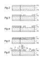
- Fig. 2 to Fig. 11 are longitudinal sectional views taken along a line A-A' of the silicon substrate 1 shown in Fig. 1 and showing first to tenth processing steps using the semiconductor and MEMS processing, respectively.
- a method of manufacturing the silicon substrate 1 will be now described with reference to Figs. 2 to 11.
- a top surface of the silicon substrate 1 will be referred to as a front surface and a bottom surface of the silicon substrate 1 will be referred to as a rear surface.
- the silicon substrate 1 having a thickness of 600 ⁇ m is prepared which has thermal oxide films 11a and 11b each of a thickness of 1.5 ⁇ m formed on the front and rear surfaces, respectively.
- a resist mask 2 is formed which has a predetermined mask pattern for forming the narrow rectangular groove 12 having the large depth h 1 , and the grooves 14a, 14b, and 14c having depths slightly larger than the depth h 1 by a micro loading effect to be described later.
- the thermal oxide film 11a of the thickness of 1.5 ⁇ m is etched away by a reactive ion etching method using electron cyclotron resonance which is one of dry etching methods (hereinafter, referred to as an ECR-RIE method).
- ECR-RIE method reactive ion etching method using electron cyclotron resonance which is one of dry etching methods
- the resist mask 2 used in the steps of Fig. 4 is removed, and a resist 3 is coated on the entire front surface of the silicon substrate 1 on which the thermal oxide film 11a is formed.
- the resist 3 formed in the steps of Fig. 5 is photoengraved so as to form the following:
- the silicon substrate 1 is subjected to deep etching from its front surface by 89 ⁇ m using a reactive ion etching method using an inductively coupled plasma as an active source and alternately performing etching and sidewall protection in a short period of time, which is one of the dry etching methods related to the semiconductor and MEMS processing (hereinafter, referred to as an ICP-RIE method), and this leads to that a sidewall protection film 7 is formed on each of the grooves including the narrow rectangular groove 12.
- ICP-RIE method dry etching methods related to the semiconductor and MEMS processing
- parts of the thermal oxide film 11a which is to serve as the narrow rectangular groove 13 and the bonding marks 15 and 16 are removed by the ECR-RIE method. Further, as shown in Fig. 9, the resist mask 3 is removed, and the sidewall protection films 7 formed during the etching in the steps of Fig. 7 are removed by a dipping treatment using a liquid mixture of a sulfuric acid and a hydrogen peroxide at 120°C.
- the silicon substrate 1 is subjected to deep etching again from its front surface by 201 ⁇ m by the ICP-RIE method while using the thermal oxide film 11a as a mask pattern, and this leads that the sidewall protection film 7 is formed on each of the grooves including the narrow rectangular groove 12.
- the narrow rectangular grooves 12 and 13 having the minute widths different from each other are formed in the surface of the silicon substrate 1, and further, the bonding marks 15 and 16 are formed as shown in Fig. 1. In this case, as shown in Fig.
- the narrow rectangular groove 12 is formed on one side of the rectangular waveguide 100 so as to be orthogonal to the narrow rectangular groove 13, and to have the depth of 290 ⁇ m and the width of 201 ⁇ m.
- the narrow rectangular groove 13 includes the first part 13a having the depth of 201 ⁇ m and the width of 201 ⁇ m and the second part 13b having the depth of 250 ⁇ m and the width of 402 ⁇ m. Further, as shown in Fig.
- the silicon wall portions 18a, 18b, and 18c each having a width w 10 of ⁇ g/4 are formed between the narrow rectangular groove 12 and the surrounding concave portion 14a, between the narrow rectangular groove 12 and the surrounding concave portion 14b, and the back-short portion 17 and the surrounding concave portion 14c, respectively.
- the surfaces at the sides of the surrounding concave portions 14a, 14b, and 14c of the respective silicon wall portions 18a, 18b, and 18c become open surfaces when viewed in an electric equivalent circuit.
- the back-short portion 17 is formed on the right end of the narrow rectangular groove 12 in a portion located left of the silicon wall portion 18c formed in a boundary with the surrounding concave portion 14c.
- This back-short portion 17 is formed, so that a length thereof (in a longitudinal direction of the narrow rectangular groove 12), i.e., a length from a center of the SIS device 6 mounted later to the end portion of the back-short portion 17 on the right end of the narrow rectangular groove 12 is set to substantially ⁇ g/4.
- an anti-fouling film (not shown) is formed on the silicon substrate 4, the silicon substrate 4 is cut to have a predetermined shape, the anti-fouling film is removed, the front, rear and side surfaces of the silicon substrate 1 are entirely coated with gold, and then, the silicon substrate 1 is completed.
- the steps of Fig. 11 may be executed after cutting the silicon substrate 1.
- the silicon substrate 1 has the narrow rectangular grooves 12 and 13 having depths different from each other, respectively, which are orthogonal to each other and formed in the surface of the silicon substrate 1.
- the formation of the narrow rectangular grooves 12 and 13 orthogonal to each other and having different depths of the present embodiment will be further described in comparison with a comparative example.
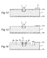
- Figs. 12 to 14 are longitudinal sectional views which are taken along a line D-D' of the silicon substrate 1 shown in Fig. 1 and which illustrate first to third processing steps using the semiconductor and MEMS processing in the comparative example.
- the deep etching of the silicon substrate 1 is performed by using the ICP-RIE method that is reactive ion etching technique for alternately performing etching and sidewall protection in a short period of time.
- Figs. 12 to 14 illustrate an instance in which silicon substrate 1 is etched simply to have multiple stages and to form minute width grooves having different depths and orthogonal to each other.
- the sidewall protection films 7 and the silicon of the silicon substrate 1 are different from each other in etching rate by several tens of times, i.e., the etching rate for the sidewall protection films 7 is lower than that for the silicon of the silicon substrate 1.
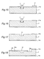
- Figs. 15 to 18 illustrate longitudinal sectional views which are taken along the line D-D' of the silicon substrate 1 shown in Fig. 1 and which illustrate first to fourth processing steps using the semiconductor and MEMS processing.
- a step of removing the sidewall protection films 7 formed on groove sidewalls during silicon etching using the ICP-RIE method is added between the steps of Fig. 13 and the steps of Fig. 14 in the comparative example (that is, between the steps of Fig. 16 and the steps of Fig. 18 in the present embodiment). Therefore, as shown in Fig.
- the dipping treatment for dipping the silicon substrate 1 in the liquid mixture of the sulfuric acid and the hydrogen peroxide at 120°C for five minutes is performed to remove the sidewall protection films 7.
- the other method of removing the sidewall protection films 7 that does not damage the silicon substrate 1 e.g., a removal treatment by the dry process using O 2 plasma, may be conducted.
- the processing of the second-stage deep etching to the silicon substrate 1 should be performed for quite a long time, it is more preferable to add the step of removing the sidewall protection films 7 halfway along the etching.
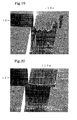
- Fig. 19 shows a scanning electron microscope photograph which shows the intersection between the narrow rectangular groove 12 for rectangular waveguide and the first part 13a of the SIS device substrate insertion narrow rectangular groove 13 of Fig. 1 when the processing steps of the comparative example shown in Figs. 12 to 14 are employed.
- Fig. 20 shows a scanning electron microscope photograph which shows the intersection between the narrow rectangular groove 12 for rectangular waveguide and the first part 13a of the narrow rectangular groove 13 for inserting the SIS device substrate, which are shown in Fig. 1, when the processing steps of the embodiment shown in Figs. 15 to 18 are employed.
- projecting silicon residues 9 are present in large quantities at the intersection.
- the projecting silicon resides 9 are hardly present at the intersection but narrow rectangular grooves 12 and 13 of fine minute width are formed.
- Fig. 21 is a perspective view showing details of the silicon substrate 4 shown in Fig. 1.
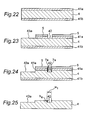
- Figs. 22 to 25 are longitudinal sectional views which are taken along a line B-B' of the silicon substrate 4 shown in Fig. 21 and which illustrate first to fourth processing steps using the semiconductor and MEMS processing. Referring to Figs. 21 to 25, a method of manufacturing the silicon substrate 4 will be described.
- Fig. 21 shows that the silicon substrate 4 is turned upside down, so that its top surface becomes a bottom surface and its bottom surface becomes a top surface.
- the top surface of the silicon substrate 4 will be referred to as the front surface, and the bottom surface thereof will be referred to as the rear surface.
- the silicon substrate 4 having a thermal oxide film 41a of a thickness of 1.5 ⁇ m formed on the front surface and a thermal oxide film 41b of a thickness of 1.5 ⁇ m formed on the rear surface, and having a thickness of 600 ⁇ m.
- a resist mask 5 is photoengraved, the thermal oxide film 41a is etched by a thickness of 1.5 ⁇ m by the ECR-RIE method using this resist mask 5, and a laminate mask including the thermal oxide film 41a and the resist mask 5 is formed.
- the silicon substrate 4 is subjected to deep etching by 290 ⁇ m from its front surface by the ICP-PIE method.
- sidewall protection films 7a are formed on sidewalls of the respective grooves including the narrow rectangular groove 42.
- the sidewall protection films 7a on the grooves other than the minute width protection groove 42 are not shown.
- the yoke insertion grooves 43a and 43b are formed at positions near the right end portion of the narrow rectangular groove 42 and in the vicinity of the SIS device when the SIS device substrate 60 is mounted during bonding of the silicon substrate 4 with the silicon substrate 1.
- the bonding marks 44 and 45 are formed at positions at which the marks 44 and 45 opposes to the bonding marks 15 and 16 of the silicon substrate 1, respectively, and on the side edges of the two sides of the silicon substrate 4 which do not oppose to each other.
- the resist mask 5 there are removed the resist mask 5, the thermal oxide films 41a and 41b, and the sidewall protection films 7a formed during the silicon deep etching by the ICP-RIE method.
- a predetermined anti-fouling film (not shown) is formed on the silicon substrate 4, the silicon substrate 4 is cut to have a predetermined shape, and the anti-fouling film is removed. Finally, the front, rear and side surfaces of the silicon substrate 4 are entirely coated with gold, and then, completing the silicon substrate 4.
- the processing steps of Fig. 25 may be executed after cutting the silicon substrate 4.
- the silicon substrates, on which the thermal oxide films 11a, 11b, 41a and 41b each having a thickness of 1.5 ⁇ m are formed on the both surfaces, respectively, are used as the silicon substrates 1 and 4.
- the present invention is not limited to this.
- the thicknesses of these thermal oxide films 11a, 11b, 41a and 41b are preferably set based on all of the depths of the narrow rectangular grooves of silicon, the etching rate, the thicknesses of the resists, and the like.
- a pair of silicon substrates 1 and 4 are used, and the narrow rectangular groove 12 for rectangular waveguide and the narrow rectangular groove 13 for inserting the SIS device, which are different from each other in depth and orthogonal to each other, are integrally formed using the ICP-RIE method based on the semiconductor and MEMS processing, by removing the projecting silicon residues 9 in the portion in which both of the narrow rectangular grooves 12 and 13 intersect each other, bonding the silicon substrate 1 onto the silicon substrate 4, on which the bonding marks 44 and 45 are formed, by adhesive or the like using the bonding marks 15 and 16. This leads to completion of the silicon substrate apparatus for the SIS mixer device.
- the narrow rectangular grooves 12 and 13 intersecting each other, having different depths, and having substantially perpendicular wall surfaces using the ICP-RIE method which is the dry etching method related to the semiconductor and MEMS processing, formation precision and intersection precision for the narrow rectangular grooves 12 and 13 can be remarkably improved as compared with the machining method.
- the narrow rectangular groove 42 having substantially perpendicular wall surfaces, and the bonding marks 44 and 45 are simultaneously formed on the other silicon substrate 4 bonded onto the silicon substrate 1.
- the rectangular waveguide 100 can be constituted in a state in which the narrow rectangular grooves 12 and 42 having rectangular cross sections oppose to each other.
- the wall surfaces of the grooves can be formed to have substantially perpendicular rectangles. Therefore, it is possible to form the rectangular waveguide 100 a cross section of which is substantially rectangular and which exhibits quite a transmission efficiency higher than that of the prior art.
- the paired silicon substrates 1 and 4 can be bonded onto each other, so that the narrow rectangular grooves 12 and 42 accurately oppose to each other at a predetermined position using the bonding marks 15 and 16, and 44 and 45 formed during the formation of the narrow rectangular grooves 12, 13, and 42, and this leads to improvement in the bonding precision.
- a progressive wave and a reflected wave can be incident onto the SIS device 6 in a predetermined phase relationship kept therebetween, and the frequency conversion efficiency of the SIS device 6 can be improved as compared with the prior art. Due to this, a reception sensitivity of the SIS mixer device for the high frequency received signal can be improved, and the reliability of the SIS mixer device can be greatly improved accordingly.
- the silicon substrates 1 and 4 can be formed by one processing using the dry etching method related to the semiconductor and MEMS processing, the productivity can be greatly improved as compared with the prior art and it is possible to provide the SIS mixer device capable of mass producing the waveguides.
- the yoke insertion grooves 43a and 43b for inserting the superconducting magnet yokes 143a and 143b for applying the magnetic fields to the SIS device 6 mounted on the SIS device substrate 60 contained in the first part 13a of the narrow rectangular groove 13 of the silicon substrate 1 are formed on the silicon substrate 4.
- the yoke insertion grooves 43a and 43b are formed at positions quite in the vicinity of the SIS device 6 mounted on the SIS device substrate 60.
- a distance between a tip end of each of the superconducting magnet yokes 143a and 143b and the center of the inserted SIS device 6 is set to 0.6 mm. Therefore, magnetic fields having an intensity of 79.6 ⁇ 10 6 [A/m] sufficient to suppress the Josephine effect of the SIS device 6 can be applied. According to the prior art, by contrast, the distance is about several millimeters. Compared with the prior art, it is possible to apply quite efficiently necessary magnetic fields to the SIS device 6 and to save power consumption in the present embodiment.
- the high frequency received signal incident from the horn antenna 8 passes through and propagates in the rectangular waveguide 100 including the paired narrow rectangular grooves 12 and 42, and then, the same signal is incident onto the SIS device 6 as formed on the SIS device substrate 60, passes through the SIS device 6, and is incident onto the back-short portion 17 provided in the rear portion which is on the right side in Fig. 1.
- the back-short portion 17 reflects this high frequency received signal on the end surface at the side of the silicon wall portion 18c of the back short portion 17 to feed the same signal to the SIS device 6 again.
- the rectangular waveguide 12 and the back-short portion 17 are constituted, so that the signal having the substantially maximum amplitude of a standing wave formed by the progressive wave and the reflected wave of the high frequency received signal arrives at the SIS device 6, and has an optimum impedance against the high frequency received signal.
- the back-short portion 17 can be formed using the ICP-RIE method related to the semiconductor and MEMS processing with higher processing precision as compared with the prior art and substantially as designed.
- a tuning mechanism for optimizing the distance of the back-short portion provided on the rectangular waveguide made of metal is not specially required in a manner different from that of the prior art. As a result, it is unnecessary to assemble the back-short portion including a plurality of members and it is possible to greatly decrease the number of parts of the back-short portion.
- the narrow rectangular groove 13 for inserting the SIS device includes the first part 13a that contains therein the SIS device 60 on which the SIS device 6 is mounted, and the second part 13b having the width w 3 larger than the width w 2 of the first part 13a so as to attach (handle) the SIS device substrate 60.
- the ICP-RIE method that is the dry etching method related to the semiconductor and MEMS processing has the micro-loading effect that the etching rate is higher in a part of the mask having a larger opening width as is well known to the art.
- the second part 13b having the width larger than that of the first part 13a is caved so as to be deeper than the first part 13a, and then, generating a height difference between the first part 13a and the second part 13b.
- the depths h 2 and h 3 of the parts 13a and 13b are 201 ⁇ m and 250 ⁇ m, respectively.
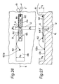
- Fig. 26 is a plan view taken along the line B-B' of Fig. 1 and showing a structure of a neighborhood of the SIS device substrate 60 in the comparative example.
- Fig. 27 is a longitudinal sectional view taken along a line E-E' of Fig. 26. Namely, Figs. 26 and 27 illustrate an instance in which the above-mentioned micro-loading effect is not considered and in which a bonding part 62b at the side of SIS device 6 of the grounding lead wire 62 is located in the part 13b of the narrow rectangular groove for inserting the SIS device.
- the grounding lead wire 62 is bonded onto the SIS device substrate 60, the SIS device substrate 60 is in a cantilever state and a break 64 occurs in the SIS device substrate 60.
- Fig. 28 is a plan view taken along the line B-B of Fig. 1 and showing a structure in the vicinity of the SIS device substrate 60 in the first implemental example of the present embodiment.
- Fig. 29 is a longitudinal sectional view taken along a line F-F' of Fig. 28.
- an entire area (an area in the longitudinal direction) of the first part 13a of the narrow rectangular groove 13 that contains therein the SIS device substrate 60 other than the portion in which the narrow rectangular groove 13 intersects the narrow rectangular groove 12 for rectangular waveguide is formed to have the equal width w 2 .
- the entire area of the first part 13a of the narrow rectangular groove 13 other than the portion in which the narrow rectangular groove 13 intersects the narrow rectangular groove 12 for rectangular waveguide has the equal depth h 2 .
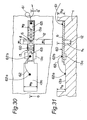
- Fig. 30 is a plan view taken along the line B-B of Fig. 1 and showing a structure in the vicinity of the SIS device substrate 60 in the second implemental example of the present embodiment.
- Fig. 31 is a longitudinal sectional view taken along a line G-G' of Fig. 30.
- a tool insertion groove 13c used upon bonding the grounding lead wire 62 is formed substantially in the central portion of the narrow rectangular groove 13 (at a position slightly shifted right from the left end portion of the first part 13a).
- This tool insertion groove 13c has a width larger than the width w 2 of the first part 13a of the narrow rectangular groove 13.
- the left end portion of the SIS device substrate 60 is mounted on a portion (in the first part 13a) having the same width as that of the width w 2 of the first part 13a.
- the bonding part 62b at the side of the SIS device substrate 6 of the grounding lead wire 62 is located on the top surface of the SIS device substrate 60 above the tool insertion groove 13c. Accordingly, as shown in Fig. 31, it is possible to prevent the SIS device substrate 60 from turning into the cantilever state when the SIS device substrate 60 is mounted on the bench portion of the first part 13a of the narrow rectangular groove 13, to prevent the break occurring during the mounting of the SIS device substrate 60 and wire-bonding, thereby improving the reliability of the apparatus.
- the structure of the first part 13a of the narrow rectangular groove 13 on the left end portion of the SIS device substrate 60 is described.
- This structure may be applied to the first part 13a of the narrow rectangular groove 13 on the right end portion of the SIS device substrate 60. That is, it is preferable that the groove width of the first part 13a of the narrow rectangular groove 13 on both end portions of the SIS device substrate 60 is at least set to the groove width w 2 of the first part 13a that is the groove width of the part which occupies most of the first part 13a in the longitudinal direction of the first part 13a.
- the yoke insertion grooves 43a and 43b for inserting the superconducting magnet yokes are formed in the silicon substrate 4.
- the yoke insertion grooves 43a and 43b for inserting the superconducting magnet may be formed at the positions in the vicinity of the SIS device 6 on the silicon substrate 1. Further, the yoke insertion grooves 43a and 43b for inserting the superconducting magnet yokes may be formed in the silicon substrates 1 and 4, respectively.
- a silicon substrate apparatus which includes a first silicon substrate, a second silicon substrate, and a device substrate.
- a first narrow rectangular groove is formed so as to have a rectangular cross section
- a second narrow rectangular groove is formed so as to be substantially orthogonal to the first narrow rectangular groove, and to have a rectangular cross section.
- a third narrow rectangular groove is formed at a position facing the first narrow rectangular groove so as to have a rectangular cross section.
- the device substrate includes a frequency conversion device, and is provided in the second narrow rectangular groove, so that the frequency conversion device is located in a portion in which the first and second narrow rectangular grooves are orthogonal to each other.
- the first silicon substrate on which the device substrate is provided is bonded onto the second silicon substrate, so that the first narrow rectangular groove opposes to the third narrow rectangular groove to each other, and then, a rectangular waveguide is formed which includes the first narrow rectangular groove and the third narrow rectangular groove.
- a high frequency received signal propagates to be incident onto the frequency conversion device.
- the silicon substrate apparatus which can be used at a cryogenic temperature that is the temperature of the environment under such a state that the high frequency receiver is used, and which can mass-produce rectangular waveguides with precision higher than that of the prior art. Further, by forming the rectangular waveguide with higher precision, it is possible to greatly improve transmission efficiency upon transmitting the high frequency received signal to the frequency conversion device through the rectangular waveguide, as compared with the prior art. It is thereby possible to improve a reception sensitivity of the SIS mixer device that employs the silicon substrate apparatus for the high frequency received signal and to greatly improve the reliability of the SIS mixer device.
- a method of manufacturing a silicon substrate apparatus which includes the following first, second, third and fourth steps.
- a first narrow rectangular groove is formed on a first silicon substrate so as to have a rectangular cross section
- a second narrow rectangular groove is formed on the first silicon substrate so as to be substantially orthogonal to the first narrow rectangular groove, and to have a rectangular cross section.
- a third narrow rectangular groove is formed on the second silicon substrate at a position facing the first narrow rectangular groove so as to have a rectangular cross section.
- a device substrate which includes a frequency conversion device in the second narrow rectangular groove, so that the frequency conversion device is located in a portion in which the first and second narrow rectangular grooves are orthogonal to each other.
- the first silicon substrate on which the device substrate is provided is bonded onto the second silicon substrate, so that the first narrow rectangular groove opposes to the third narrow rectangular groove to each other, and then, a rectangular waveguide is formed which includes the first narrow rectangular groove and the third narrow rectangular groove, in which a high frequency received signal propagates to be incident onto the frequency conversion device.
- the method of manufacturing the silicon substrate apparatus which can be used at a cryogenic temperature that is the temperature of the environment under such a state that the high frequency receiver is used, and which can mass-produce rectangular waveguides with precision higher than that of the prior art. Further, by forming the rectangular waveguide with higher precision, it is possible to greatly improve transmission efficiency upon transmitting the high frequency received signal to the frequency conversion device through the rectangular waveguide, as compared with the prior art. It is thereby possible to improve a reception sensitivity of the SIS mixer device that employs the silicon substrate apparatus for the high frequency received signal and to greatly improve the reliability of the SIS mixer device.
- a method of manufacturing a silicon substrate apparatus which includes a step of forming first and second narrow rectangular grooves on a silicon substrate using a dry etching method for a semiconductor and MEMS (Micro Electro Mechanical Machining) processing.
- the first narrow rectangular groove has a rectangular cross section.
- the second narrow rectangular groove is substantially orthogonal to the first narrow rectangular groove, has a depth different from a depth of the first narrow rectangular groove, and has a rectangular cross section,
- the first and second narrow rectangular grooves intersecting each other and having different depths on the silicon substrate by the dry etching method for the semiconductor and MEMS (Micro Electro Mechanical Systems) processing, the first and second narrow rectangular grooves can be formed with precision higher than that of the prior art. Besides, since the silicon substrates can be formed by one processing, the productivity can be greatly improved as compared with the prior art.
- MEMS Micro Electro Mechanical Systems
- the method of manufacturing the silicon substrate apparatus it is preferable that in the above-mentioned step, when the first and second narrow rectangular grooves are formed in a plurality of stages by the dry etching method, sidewall protection films are formed on sidewalls of the first and second narrow rectangular grooves, respectively.
- the method further includes a step of removing the respective sidewall protection films after a processing of forming the first and second narrow rectangular grooves by the dry etching method in each of the stages.
Landscapes
- Physics & Mathematics (AREA)
- Electromagnetism (AREA)
- Engineering & Computer Science (AREA)
- Power Engineering (AREA)
- Micromachines (AREA)
- Optical Integrated Circuits (AREA)
- Waveguides (AREA)
Applications Claiming Priority (1)
| Application Number | Priority Date | Filing Date | Title |
|---|---|---|---|
| PCT/JP2002/008964 WO2004023644A1 (ja) | 2002-09-04 | 2002-09-04 | シリコン基板装置とその製造方法 |
Publications (3)
| Publication Number | Publication Date |
|---|---|
| EP1536555A1 true EP1536555A1 (de) | 2005-06-01 |
| EP1536555A4 EP1536555A4 (de) | 2005-12-21 |
| EP1536555B1 EP1536555B1 (de) | 2010-08-04 |
Family
ID=31972298
Family Applications (1)
| Application Number | Title | Priority Date | Filing Date |
|---|---|---|---|
| EP02807763A Expired - Lifetime EP1536555B1 (de) | 2002-09-04 | 2002-09-04 | Einrichtung mit siliziumsubstrat und verfahren zu ihrer herstellung |
Country Status (5)
| Country | Link |
|---|---|
| US (1) | US7081370B2 (de) |
| EP (1) | EP1536555B1 (de) |
| JP (1) | JP4209842B2 (de) |
| DE (1) | DE60237239D1 (de) |
| WO (1) | WO2004023644A1 (de) |
Cited By (1)
| Publication number | Priority date | Publication date | Assignee | Title |
|---|---|---|---|---|
| CN101707276B (zh) * | 2009-12-10 | 2012-08-29 | 中国航天科工集团第二研究院二○三所 | 一种波导单端口失配器的设计方法 |
Families Citing this family (8)
| Publication number | Priority date | Publication date | Assignee | Title |
|---|---|---|---|---|
| US7341946B2 (en) * | 2003-11-10 | 2008-03-11 | Novellus Systems, Inc. | Methods for the electrochemical deposition of copper onto a barrier layer of a work piece |
| US7439093B2 (en) * | 2005-09-16 | 2008-10-21 | Dalsa Semiconductor Inc. | Method of making a MEMS device containing a cavity with isotropic etch followed by anisotropic etch |
| JP5036614B2 (ja) * | 2008-04-08 | 2012-09-26 | 東京応化工業株式会社 | 基板用ステージ |
| US8080774B1 (en) * | 2008-08-12 | 2011-12-20 | Hrl Laboratories, Llc | Module for scalable millimeter wave imaging arrays |
| US8168464B2 (en) * | 2010-01-25 | 2012-05-01 | Freescale Semiconductor, Inc. | Microelectronic assembly with an embedded waveguide adapter and method for forming the same |
| DE102012203293B4 (de) | 2012-03-02 | 2021-12-02 | Robert Bosch Gmbh | Halbleitermodul mit integriertem Wellenleiter für Radarsignale |
| WO2014137484A1 (en) * | 2013-03-08 | 2014-09-12 | Northrop Grumman Systems Corporation | Waveguide and semiconductor packaging |
| TWI806615B (zh) * | 2022-05-19 | 2023-06-21 | 國立清華大學 | 濾波器及其製造方法 |
Family Cites Families (14)
| Publication number | Priority date | Publication date | Assignee | Title |
|---|---|---|---|---|
| US3970965A (en) * | 1975-03-26 | 1976-07-20 | The United States Of America As Represented By The Secretary Of The Navy | Injection locked Josephson oscillator systems |
| US4229828A (en) * | 1977-12-23 | 1980-10-21 | Hughes Aircraft Company | Bi-mode millimeter wave mixer |
| DE3737671A1 (de) * | 1987-11-06 | 1989-05-24 | Ant Nachrichtentech | Mikrowellen-gegentaktmischer |
| EP0372951B1 (de) * | 1988-12-09 | 1996-08-14 | Canon Kabushiki Kaisha | Supraleitender elektromagnetischer Wellenmischer und diesen enthaltendes Gerät |
| JPH0563409A (ja) | 1991-08-29 | 1993-03-12 | Nissan Motor Co Ltd | 導波管 |
| DE4241045C1 (de) * | 1992-12-05 | 1994-05-26 | Bosch Gmbh Robert | Verfahren zum anisotropen Ätzen von Silicium |
| JPH06216653A (ja) | 1993-01-20 | 1994-08-05 | Fujitsu Ltd | 導波管型ミキサおよびその製造方法 |
| JPH08111547A (ja) | 1994-10-06 | 1996-04-30 | Fujitsu Ltd | Sisミクサ回路 |
| US5757243A (en) * | 1995-05-25 | 1998-05-26 | Matsushita Electric Industrial Co., Ltd. | High frequency system including a superconductive device and temperature controlling apparatus |
| JP3119191B2 (ja) | 1997-02-27 | 2000-12-18 | 株式会社村田製作所 | 平面誘電体集積回路 |
| JPH11168172A (ja) * | 1997-12-04 | 1999-06-22 | Toshiba Tec Corp | 半導体チップの製造方法及びその半導体チップによる3次元構造体、その製造方法及びその電気的接続方法 |
| US6902328B2 (en) * | 2001-07-30 | 2005-06-07 | Matsushita Electric Industrial Co., Ltd. | Optical module and manufacturing method thereof |
| JP4240890B2 (ja) * | 2002-02-06 | 2009-03-18 | 沖電気工業株式会社 | 光学素子の製造方法および光学素子 |
| US6944377B2 (en) * | 2002-03-15 | 2005-09-13 | Hitachi Maxell, Ltd. | Optical communication device and laminated optical communication module |
-
2002
- 2002-09-04 WO PCT/JP2002/008964 patent/WO2004023644A1/ja not_active Ceased
- 2002-09-04 US US10/492,360 patent/US7081370B2/en not_active Expired - Lifetime
- 2002-09-04 DE DE60237239T patent/DE60237239D1/de not_active Expired - Lifetime
- 2002-09-04 JP JP2004534067A patent/JP4209842B2/ja not_active Expired - Fee Related
- 2002-09-04 EP EP02807763A patent/EP1536555B1/de not_active Expired - Lifetime
Cited By (1)
| Publication number | Priority date | Publication date | Assignee | Title |
|---|---|---|---|---|
| CN101707276B (zh) * | 2009-12-10 | 2012-08-29 | 中国航天科工集团第二研究院二○三所 | 一种波导单端口失配器的设计方法 |
Also Published As
| Publication number | Publication date |
|---|---|
| DE60237239D1 (de) | 2010-09-16 |
| WO2004023644A1 (ja) | 2004-03-18 |
| JPWO2004023644A1 (ja) | 2006-01-05 |
| US7081370B2 (en) | 2006-07-25 |
| US20050009226A1 (en) | 2005-01-13 |
| EP1536555A4 (de) | 2005-12-21 |
| EP1536555B1 (de) | 2010-08-04 |
| JP4209842B2 (ja) | 2009-01-14 |
Similar Documents
| Publication | Publication Date | Title |
|---|---|---|
| EP1396902B1 (de) | Hohlleiter/mikrostreifenleitungswandler | |
| Alonso-del Pino et al. | Micromachining for advanced terahertz: Interconnects and packaging techniques at terahertz frequencies | |
| US10364144B2 (en) | Hermetically sealed package for mm-wave molecular spectroscopy cell | |
| CA1323913C (en) | Broadband microstrip to coplanar waveguide transition by anisotropic etching of gallium arsenide | |
| US20130229210A1 (en) | On-chip power-combining for high-power schottky diode based frequency multipliers | |
| EP1536555B1 (de) | Einrichtung mit siliziumsubstrat und verfahren zu ihrer herstellung | |
| CN111211394A (zh) | 同轴-波导管转换器阵列、天线阵列及波导装置的制造方法 | |
| CN104467681B (zh) | 基于单片集成电路的太赫兹分谐波倍频混频装置 | |
| US7899432B2 (en) | Submillimeter wave heterodyne receiver | |
| CN110854549A (zh) | 天线阵列以及通信系统 | |
| US20090246929A1 (en) | Membrane suspended mems structures | |
| JP4753981B2 (ja) | 導波管・ストリップ線路変換器 | |
| US6404402B1 (en) | Preferential crystal etching technique for the fabrication of millimeter and submillimeter wavelength horn antennas | |
| JPH09246816A (ja) | 導波管−マイクロストリップ線路変換器 | |
| Bacha et al. | LSE-mode balun for hybrid integration of NRD-guide and microstrip line | |
| US12519070B2 (en) | System, electronic device and package with vertical to horizontal substrate integrated waveguide transition and horizontal grounded coplanar waveguide transition | |
| US10923790B2 (en) | Low-loss silicon on insulator based dielectric microstrip line | |
| EP4262013B1 (de) | Hybride struktur für ultrabreitband terahertzerzeugung und -empfang mit halbleiterbauelementen | |
| Drayton et al. | Micromachined circuits for Mm-wove applications | |
| US7418164B2 (en) | Method for forming a photonic band-gap structure and a device fabricated in accordance with such a method | |
| US7342469B2 (en) | Air cavity module for planar type filter operating in millimeter-wave frequency bands | |
| US6229411B1 (en) | Integral waveguide structure and semiconductor wafer | |
| JP3136386B2 (ja) | プラズマ処理装置 | |
| JP2949068B2 (ja) | 高周波用伝送線路の製造方法 | |
| Schur et al. | Micromachined split-block Schottky-diode mixer for 600 GHz |
Legal Events
| Date | Code | Title | Description |
|---|---|---|---|
| PUAI | Public reference made under article 153(3) epc to a published international application that has entered the european phase |
Free format text: ORIGINAL CODE: 0009012 |
|
| 17P | Request for examination filed |
Effective date: 20040504 |
|
| AK | Designated contracting states |
Kind code of ref document: A1 Designated state(s): AT BE BG CH CY CZ DE DK EE ES FI FR GB GR IE IT LI LU MC NL PT SE SK TR |
|
| A4 | Supplementary search report drawn up and despatched |
Effective date: 20051107 |
|
| RBV | Designated contracting states (corrected) |
Designated state(s): DE FR GB NL |
|
| RAP1 | Party data changed (applicant data changed or rights of an application transferred) |
Owner name: MITSUBISHI DENKI KABUSHIKI KAISHA |
|
| 17Q | First examination report despatched |
Effective date: 20060428 |
|
| GRAJ | Information related to disapproval of communication of intention to grant by the applicant or resumption of examination proceedings by the epo deleted |
Free format text: ORIGINAL CODE: EPIDOSDIGR1 |
|
| GRAP | Despatch of communication of intention to grant a patent |
Free format text: ORIGINAL CODE: EPIDOSNIGR1 |
|
| GRAJ | Information related to disapproval of communication of intention to grant by the applicant or resumption of examination proceedings by the epo deleted |
Free format text: ORIGINAL CODE: EPIDOSDIGR1 |
|
| GRAP | Despatch of communication of intention to grant a patent |
Free format text: ORIGINAL CODE: EPIDOSNIGR1 |
|
| GRAP | Despatch of communication of intention to grant a patent |
Free format text: ORIGINAL CODE: EPIDOSNIGR1 |
|
| GRAS | Grant fee paid |
Free format text: ORIGINAL CODE: EPIDOSNIGR3 |
|
| RIN1 | Information on inventor provided before grant (corrected) |
Inventor name: HONMA, YUKIHIRO,MITSUBISHI DENKI K. K. Inventor name: YOSHIDA, YUKIHISA,MITSUBISHI DENKI K. K. Inventor name: MATSUURA, TSUKASA,MITSUBISHI DENKI K. K. Inventor name: KUMAGAI, MUNEHITO,MITSUBISHI DENKI K. K. |
|
| GRAA | (expected) grant |
Free format text: ORIGINAL CODE: 0009210 |
|
| AK | Designated contracting states |
Kind code of ref document: B1 Designated state(s): DE FR GB NL |
|
| REG | Reference to a national code |
Ref country code: GB Ref legal event code: FG4D |
|
| REF | Corresponds to: |
Ref document number: 60237239 Country of ref document: DE Date of ref document: 20100916 Kind code of ref document: P |
|
| REG | Reference to a national code |
Ref country code: NL Ref legal event code: T3 |
|
| REG | Reference to a national code |
Ref country code: GB Ref legal event code: S27 Free format text: APPLICATION FILED; APPLICATION TO AMEND SPECIFICATION UNDER SECTION 27 FILED ON 02 FEBRUARY 2011. |
|
| PLBE | No opposition filed within time limit |
Free format text: ORIGINAL CODE: 0009261 |
|
| STAA | Information on the status of an ep patent application or granted ep patent |
Free format text: STATUS: NO OPPOSITION FILED WITHIN TIME LIMIT |
|
| 26N | No opposition filed |
Effective date: 20110506 |
|
| REG | Reference to a national code |
Ref country code: DE Ref legal event code: R097 Ref document number: 60237239 Country of ref document: DE Effective date: 20110506 |
|
| REG | Reference to a national code |
Ref country code: GB Ref legal event code: S27 Free format text: APPLICATION OPEN FOR OPPOSITION; PATENTS FORM 15 GIVING THE COMPTROLLER NOTICE OF OPPOSITION TO THE AMENDMENTS.YOU ALSO NEED TO FILE TWO COPIES OF A STATEMENT SETTING OUR FULLY THE FACTS OF YOUR CASE AND THE RELIEF THAT YOU ARE SEEKING TITLE OF PATENT: SILICON SUBSTRATE DEVICE AND ITS MANUFACTURING METHOD INTERNATIONAL CLASSIFICATION: H03D NAME OF PROPRIETOR: MITSUBISHI DENKI KABUSHIKI KAISHA FOR A COPY OF THESE AMENDMENTS, PHONE LITIGATION SECTION (01633 814797) |
|
| REG | Reference to a national code |
Ref country code: GB Ref legal event code: S27 Free format text: SPECIFICATION AMENDED; APPLICATION FOR AMENDMENT UNDER SECTION 27 FILED ON 2 FEBRUARY 2011 ALLOWED ON 29 JUNE 2012 |
|
| REG | Reference to a national code |
Ref country code: GB Ref legal event code: 746 Effective date: 20130513 |
|
| REG | Reference to a national code |
Ref country code: DE Ref legal event code: R084 Ref document number: 60237239 Country of ref document: DE Effective date: 20130503 |
|
| REG | Reference to a national code |
Ref country code: FR Ref legal event code: PLFP Year of fee payment: 15 |
|
| REG | Reference to a national code |
Ref country code: FR Ref legal event code: PLFP Year of fee payment: 16 |
|
| REG | Reference to a national code |
Ref country code: FR Ref legal event code: PLFP Year of fee payment: 17 |
|
| REG | Reference to a national code |
Ref country code: GB Ref legal event code: S47 Free format text: CANCELLATION OF ENTRY; APPLICATION FOR CANCELLATION OF ENTRY ON THE REGISTER OF A LICENCE OF RIGHT FILED ON 06 FEBRUARY 2019 |
|
| REG | Reference to a national code |
Ref country code: DE Ref legal event code: R085 Ref document number: 60237239 Country of ref document: DE |
|
| REG | Reference to a national code |
Ref country code: GB Ref legal event code: S47 Free format text: ENTRY CANCELLED; NOTICE IS HEREBY GIVEN THAT THE LICENCE OF RIGHT ENTRY ON THE REGISTER FOR THE FOLLOWING PATENT WAS CANCELLED ON 10 MAY 2019 MITSUBISHI DENKI KABUSHIKI KAISHA SILICON SUBSTRATE DEVICE AND ITS MANUFACTURING METHOD |
|
| PGFP | Annual fee paid to national office [announced via postgrant information from national office to epo] |
Ref country code: NL Payment date: 20200814 Year of fee payment: 19 |
|
| PGFP | Annual fee paid to national office [announced via postgrant information from national office to epo] |
Ref country code: GB Payment date: 20200826 Year of fee payment: 19 Ref country code: DE Payment date: 20200826 Year of fee payment: 19 Ref country code: FR Payment date: 20200812 Year of fee payment: 19 |
|
| REG | Reference to a national code |
Ref country code: DE Ref legal event code: R119 Ref document number: 60237239 Country of ref document: DE |
|
| REG | Reference to a national code |
Ref country code: NL Ref legal event code: MM Effective date: 20211001 |
|
| GBPC | Gb: european patent ceased through non-payment of renewal fee |
Effective date: 20210904 |
|
| PG25 | Lapsed in a contracting state [announced via postgrant information from national office to epo] |
Ref country code: NL Free format text: LAPSE BECAUSE OF NON-PAYMENT OF DUE FEES Effective date: 20211001 |
|
| PG25 | Lapsed in a contracting state [announced via postgrant information from national office to epo] |
Ref country code: GB Free format text: LAPSE BECAUSE OF NON-PAYMENT OF DUE FEES Effective date: 20210904 Ref country code: FR Free format text: LAPSE BECAUSE OF NON-PAYMENT OF DUE FEES Effective date: 20210930 Ref country code: DE Free format text: LAPSE BECAUSE OF NON-PAYMENT OF DUE FEES Effective date: 20220401 |