EP1536478A2 - Solid state imaging device and producing method thereof - Google Patents
Solid state imaging device and producing method thereof Download PDFInfo
- Publication number
- EP1536478A2 EP1536478A2 EP04257300A EP04257300A EP1536478A2 EP 1536478 A2 EP1536478 A2 EP 1536478A2 EP 04257300 A EP04257300 A EP 04257300A EP 04257300 A EP04257300 A EP 04257300A EP 1536478 A2 EP1536478 A2 EP 1536478A2
- Authority
- EP
- European Patent Office
- Prior art keywords
- face
- solid state
- imaging device
- state imaging
- wafer
- Prior art date
- Legal status (The legal status is an assumption and is not a legal conclusion. Google has not performed a legal analysis and makes no representation as to the accuracy of the status listed.)
- Withdrawn
Links
Images








Classifications
-
- H—ELECTRICITY
- H10—SEMICONDUCTOR DEVICES; ELECTRIC SOLID-STATE DEVICES NOT OTHERWISE PROVIDED FOR
- H10F—INORGANIC SEMICONDUCTOR DEVICES SENSITIVE TO INFRARED RADIATION, LIGHT, ELECTROMAGNETIC RADIATION OF SHORTER WAVELENGTH OR CORPUSCULAR RADIATION
- H10F99/00—Subject matter not provided for in other groups of this subclass
-
- H—ELECTRICITY
- H10—SEMICONDUCTOR DEVICES; ELECTRIC SOLID-STATE DEVICES NOT OTHERWISE PROVIDED FOR
- H10F—INORGANIC SEMICONDUCTOR DEVICES SENSITIVE TO INFRARED RADIATION, LIGHT, ELECTROMAGNETIC RADIATION OF SHORTER WAVELENGTH OR CORPUSCULAR RADIATION
- H10F39/00—Integrated devices, or assemblies of multiple devices, comprising at least one element covered by group H10F30/00, e.g. radiation detectors comprising photodiode arrays
- H10F39/80—Constructional details of image sensors
- H10F39/809—Constructional details of image sensors of hybrid image sensors
-
- H—ELECTRICITY
- H10—SEMICONDUCTOR DEVICES; ELECTRIC SOLID-STATE DEVICES NOT OTHERWISE PROVIDED FOR
- H10F—INORGANIC SEMICONDUCTOR DEVICES SENSITIVE TO INFRARED RADIATION, LIGHT, ELECTROMAGNETIC RADIATION OF SHORTER WAVELENGTH OR CORPUSCULAR RADIATION
- H10F39/00—Integrated devices, or assemblies of multiple devices, comprising at least one element covered by group H10F30/00, e.g. radiation detectors comprising photodiode arrays
- H10F39/011—Manufacture or treatment of image sensors covered by group H10F39/12
- H10F39/018—Manufacture or treatment of image sensors covered by group H10F39/12 of hybrid image sensors
-
- H—ELECTRICITY
- H10—SEMICONDUCTOR DEVICES; ELECTRIC SOLID-STATE DEVICES NOT OTHERWISE PROVIDED FOR
- H10F—INORGANIC SEMICONDUCTOR DEVICES SENSITIVE TO INFRARED RADIATION, LIGHT, ELECTROMAGNETIC RADIATION OF SHORTER WAVELENGTH OR CORPUSCULAR RADIATION
- H10F39/00—Integrated devices, or assemblies of multiple devices, comprising at least one element covered by group H10F30/00, e.g. radiation detectors comprising photodiode arrays
- H10F39/80—Constructional details of image sensors
- H10F39/811—Interconnections
-
- H—ELECTRICITY
- H10—SEMICONDUCTOR DEVICES; ELECTRIC SOLID-STATE DEVICES NOT OTHERWISE PROVIDED FOR
- H10W—GENERIC PACKAGES, INTERCONNECTIONS, CONNECTORS OR OTHER CONSTRUCTIONAL DETAILS OF DEVICES COVERED BY CLASS H10
- H10W99/00—Subject matter not provided for in other groups of this subclass
-
- H—ELECTRICITY
- H10—SEMICONDUCTOR DEVICES; ELECTRIC SOLID-STATE DEVICES NOT OTHERWISE PROVIDED FOR
- H10F—INORGANIC SEMICONDUCTOR DEVICES SENSITIVE TO INFRARED RADIATION, LIGHT, ELECTROMAGNETIC RADIATION OF SHORTER WAVELENGTH OR CORPUSCULAR RADIATION
- H10F39/00—Integrated devices, or assemblies of multiple devices, comprising at least one element covered by group H10F30/00, e.g. radiation detectors comprising photodiode arrays
- H10F39/011—Manufacture or treatment of image sensors covered by group H10F39/12
-
- H—ELECTRICITY
- H10—SEMICONDUCTOR DEVICES; ELECTRIC SOLID-STATE DEVICES NOT OTHERWISE PROVIDED FOR
- H10F—INORGANIC SEMICONDUCTOR DEVICES SENSITIVE TO INFRARED RADIATION, LIGHT, ELECTROMAGNETIC RADIATION OF SHORTER WAVELENGTH OR CORPUSCULAR RADIATION
- H10F39/00—Integrated devices, or assemblies of multiple devices, comprising at least one element covered by group H10F30/00, e.g. radiation detectors comprising photodiode arrays
- H10F39/011—Manufacture or treatment of image sensors covered by group H10F39/12
- H10F39/026—Wafer-level processing
-
- H—ELECTRICITY
- H10—SEMICONDUCTOR DEVICES; ELECTRIC SOLID-STATE DEVICES NOT OTHERWISE PROVIDED FOR
- H10F—INORGANIC SEMICONDUCTOR DEVICES SENSITIVE TO INFRARED RADIATION, LIGHT, ELECTROMAGNETIC RADIATION OF SHORTER WAVELENGTH OR CORPUSCULAR RADIATION
- H10F39/00—Integrated devices, or assemblies of multiple devices, comprising at least one element covered by group H10F30/00, e.g. radiation detectors comprising photodiode arrays
- H10F39/80—Constructional details of image sensors
- H10F39/804—Containers or encapsulations
-
- H—ELECTRICITY
- H10—SEMICONDUCTOR DEVICES; ELECTRIC SOLID-STATE DEVICES NOT OTHERWISE PROVIDED FOR
- H10W—GENERIC PACKAGES, INTERCONNECTIONS, CONNECTORS OR OTHER CONSTRUCTIONAL DETAILS OF DEVICES COVERED BY CLASS H10
- H10W74/00—Encapsulations, e.g. protective coatings
- H10W74/10—Encapsulations, e.g. protective coatings characterised by their shape or disposition
- H10W74/15—Encapsulations, e.g. protective coatings characterised by their shape or disposition on active surfaces of flip-chip devices, e.g. underfills
Definitions
- the present invention relates to a solid state imaging device with a wafer-level chip size package, and more particularly to a solid state imaging device in which a wiring is extended to an opposite surface to a photoelectric conversion surface, and a producing method of the solid state imaging device.
- a digital video camera and a video camera with use of solid state imaging device (such as CCDs, CMOS type and the like) is in widespread use.
- an electronic apparatus (a personal computer, a mobile phone, an electronic notepads or the like) includes a solid state imaging device and a memory to have an image-taking function. Since having a large influence on an outer size of a digital camera or an electronic apparatus with the image-taking function, the solid state imaging device is required to be small.
- the solid state imaging device utilizing a packaging method called a chip size package (hereinafter CSP) is invented (for example, Japanese Utility Model Publication No. 08-005566).
- CSP chip size package
- the CSP method at first, plural image sensors are formed with a matrix arrangement on the wafer in semiconductor wafer process. Then the dicing of the wafer is made, and the wafer is cut to the bare chips having respective image sensor. The bare chip is assembled on an assembly substrate, and thereafter packaged by a plastic, such that the solid state imaging device may be obtained.
- the obtained solid state imaging device is as large as or slightly larger than the bare chip.
- the solid state imaging device utilizing a wafer-level chip size package (hereinafter WLCSP) is invented to enable smaller packaging than the CSP (for example, Japanese Patent Laid-Open Publication No.2001-351997).
- WLCSP wafer-level chip size package
- the solid state imaging device of the CSP type or the WLCSP type is assembled on a printed circuit with adhesion, and a connection terminals formed on an upper face of the solid state imaging device is connected through a bonding wire to the printed circuit board.
- the assembling size actually becomes large. Accordingly, in the solid state imaging device of the above two publications No. 08-005566 and 2001-351997, the connection terminals are formed on a lower surface by through-hole interconnections and the face bonding to the assembly substrate or the printed circuit board is made.
- the through-hole interconnections are formed before the bare chip are packaged with resin or a cover glass. Accordingly, dusts and cruds are easily adhered onto the imaging elements, and the production yield becomes lower.
- the through-hole interconnections may be formed after the bare chip are packaged. In followings, a method of producing the solid state imaging device having the through-hole interconnections is simply explained.
- a solid state imaging device 100 shown in FIGs. 14A, 14B has a semiconductor substrate 103 whose upper surface is provided with image sensor 101 and contact terminals 102, and a cover glass 105 for packaging the upper face of the semiconductor substrate (sensor chip) 103 inserting a spacer 104 between the semiconductor substrate 103 and the cover glass 105.
- the semiconductor substrate 103 has through-hole interconnections 107 for connecting a contact terminal 102 on its upper surface to a connection terminal 106 on its lower surface. Between the semiconductor substrate 103 and the through-hole interconnections 107 and between the semiconductor substrate 103 and the connection terminal 106 are respectively provided an insulation layer 117 for insulating a side wall and an insulating layer 122 for insulating a bottom.
- the treatment content is distinguished to a high temperature treatment under high temperature, a vacuum treatment under the vacuum condition, and a wet treatment made with use of a liquid.
- the treatment made in each process is marked with an asterisk.
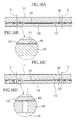
- a joint of a wafer and a glass substrate is made.
- a wafer 110 is obtained by forming plural image sensors 101 and the contact terminals 102 on the well-known silicone wafer in the semiconductor wafer process.
- the wafer 110 is cut into each image sensor 101 to be the semiconductor substrate (sensor chip) 103.
- a glass substrate 111 is a substrate of the cover glass 105, and cut together with the wafer 110 to be the cover glasses 105.
- To a bottom of the glass substrate 111 is connected to a spacer substrate 112, which is cut in the same manner to be the spacer 104.
- an adhesive agent is applied to the spacer substrate 112. After the deposition of the spacer substrate 112 on the wafer 10, they are pressed to make the adhesion and the adhesive agent is solidified. Thus, since the image sensors are packaged by the glass substrate 111 and the spacer substrate 112, the dust does not adhere to the image sensor 101 in the following process.
- a chain double dashed line X in this figure illustrates positions for cutting the wafer 110 and the glass substrate 111 at each image sensor 101.
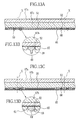
- through-holes are formed. As shown in FIG. 16C&16D, through-holes 115 are formed on a bottom of the wafer 110 so as to confront each contact terminal 102. At first, in the portions not forming the through-holes on the bottom, a resist mask is formed by a photolithography. Then the through-holes 115 are formed on the wafer 110 by the plasma etching. Through the through-holes 115, a bottom of each contact terminal 102 is exposed. The resist mask is removed by ashing.
- the insulating layer 117 is formed on a side wall of the through-holes 115.
- the insulating layer 117 is formed in a chemical vapor deposition.
- the insulating layer 117 is formed on the contact terminal 102 exposed in the through-holes 115, and therefore prevents the conduction between the contact terminal and a conductive paste filled in the through-holes 115. Accordingly, in the fourth process, the insulation layer 117 on the contact terminal 102 is removed.
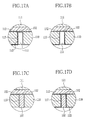
- a resist mask is formed on the bottom of the wafer 110 by a photolithography, and then the plasma etching is made to remove only the insulation layer 117 on the contact terminal which is not masked, as shown in FIG.17B.
- the resist mask is removed by ashing.
- the through-holes 115 are filled with a conductive paste for forming the through-hole interconnections 107.
- the filling of the conductive paste is made by a vacuum screen printing.
- the conductive paste in the through-hole 115 is hardened by heating the wafer 110.
- the conductive paste filled by the vacuum screen printing forms a dent on the bottom of the wafer 110.
- the grinding and the polishing namely the backgrind, is made.
- the insulating layer 117 on the bottom of the wafer 110 is removed.
- an insulating layer 122 is formed on whole of the bottom of the wafer 110.
- the plasma etching is made to whole of bottom of the wafer 110 such that the through-hole interconnections may project from the bottom as shown in FIG.17C.
- an insulating adhesive agent is applied to a bottom of the wafer 110, and solidified with heating so as to form the insulating layer 122 in FIG.17D. Since the insulating layer 122 is formed also on the through-hole interconnections 107, the backgrind is made again such that the through-hole interconnections 107 may be exposed from the insulation layer 122.
- connection terminal 106 is formed on the insulating layer 122.
- a resist mask is formed on the bottom of the wafer 110 by the photolithography, and the bottom and a side of the wafer 110 is dipped into a plating solution to make an electroless deposition, such that the connection terminal 106 may be formed.
- the solution and the like are used for the removal of the resist mask.
- the dicing of the wafer 110 and the glass substrate 111 connected thereto is made at the position of the chain double dashed line X.
- the solid state imaging device 100 of the WLCSP illustrated in FIG.14 is completed.
- a high-temperature treatment, a vacuum treatment, a wet treatment and the like are made many times as described above, for example a plasma etching, the ashing, a formation of the insulating layer, and the backgrind and the like.
- a plasma etching, the ashing, a formation of the insulating layer, and the backgrind and the like are made many times as described above, for example a plasma etching, the ashing, a formation of the insulating layer, and the backgrind and the like.
- the solid state imaging device of the CSP structure or the WLCSP structure becomes small, and therefore the pitch of interconnection is short.
- the aspect ratio of the through-hole interconnection is high.
- the through-hole interconnections easily have voids caused by insufficient supply of the conductive paste, and the voids change the resistance.
- the change of the resistance of the through-hole interconnection disrupts the output waveform, and the image quality became worse.
- An object of the present invention is to provide a solid state imaging device, in which interconnections can be exposed on a bottom of the semiconductor substrate in a low cost.
- a solid state imaging device of the present invention includes a semiconductor substrate having first and second faces, a translucent member superimposed on the first face of the semiconductor substrate, and an assembly substrate for assembling the semiconductor substrate thereon.
- the first face of the semiconductor substrate is provided with plural image sensors and plural contact terminals connected to the respective image sensors.
- the each contact terminal appears through the through-holes formed by piercing from a side of the second face.
- the translucent member is superimposed on the first face of the semiconductor substrate, the image sensors and the contact terminals are sealed.
- plural bumps are formed in at least one of the semiconductor substrate and the assembly substrate for connecting the contact terminal in the each through-hole to the assembly substrate.
- a solid state imaging device of the present invention includes a semiconductor substrate having first and second faces, a translucent member superimposed on the first face of the semiconductor substrate, and an assembly substrate for assembling the semiconductor substrate thereon.
- the first face of the semiconductor substrate is provided with plural image sensors and plural contact terminals connected to the respective image sensors.
- the each contact terminal appears through the through-holes on the second face of the semiconductor substrate.
- the image sensors and the contact terminals are sealed.
- plural bumps are positioned in the respective through-holes for connecting the contact terminal in each through-hole and the connection terminal.
- peripheral circuitry when a pattern of peripheral circuitry is formed on the second face, electric parts for the peripheral circuitry can be assembled.
- the translucent member is one of a low- ⁇ -ray glass, IR-cut filter and a low path filter.
- the translucent member is attached to the semiconductor substrate through the spacer, whose material is one of stainless and silicon.
- the semiconductor substrate is from 30 to 100 ⁇ m in thickness.
- plural units constructed of plural image sensors and plural contact terminals respectively connected to the image sensors are formed on a first face of a wafer.
- a translucent substrate is joined onto the first face of the wafer to seal the image sensor and the contact terminals.
- plural through-holes are formed from a side of the second face such that the plural contact terminals may appear on the second face.
- the joined wafer and the translucent substrate are cut at each of the units such that plural semiconductor substrates may be obtained, each of which has the image sensors.
- Bumps are formed on an assembly substrate, on which the semiconductor substrate is assembled so as to contact the contact terminal in the each through-hole to the assembly substrate through the bump.
- plural units constructed of plural image sensors and plural contact terminals respectively connected to the image sensors are formed on a first face of a wafer.
- a translucent substrate is joined onto the first face of the wafer to seal the image sensor and the contact terminals.
- plural through-holes are formed from a side of the second face such that the plural contact terminals may appear on the second face.
- Bumps are formed in the respective through-holes.
- Plural connection terminals are formed on the second face of the wafer so as to connect the connection terminal and the contact terminals through the bumps. Them the joined wafer and translucent substrate are cut for each image sensor.
- the solid state imaging device and a producing method thereof since the bumps are used instead of through-hole interconnections, the deterioration of the image quality caused by the voids in the through-hole interconnections does not occur. Further, the operations of the high cost, for example the insulation layer in the through-hole, the remove of the insulation layer on the contact terminal, vacuum screen print and the like can be omitted, the number of the operations can be reduced and the solid state imaging device can be produced in low cost.
- the grinding of the wafer is made before forming the through-holes, the thickness of the solid state imaging device can be decreased. Further, since the etching for forming the through-holes can be completed in a sort time, the productivity becomes higher, the cost becomes lower, and the side etch is prevented. If the grinding of only the wafer is made, the strength extremely decreases, and therefore the handling and the like are difficult. However, since the grinding of the wafer joined to the translucent substrate, the strength can be kept enough for the handling.
- the apparatus in which the solid state imaging device is used can become smaller. Further, since the contact terminals are sealed by the translucent member, the width of sealing becomes larger. Therefore the sealing effective increases.
- the solid state imaging device Since there is a space between the image sensor and the translucent member, the solid state imaging device is provided with micro lenses above respective pixels having photoelectric function, and the effectives of the micro lenses don't become lower.
- the said translucent member is one of a low- ⁇ -ray glass, IR-cut filter and a low path filter, an space and works for attachment can be made smaller than when they are separately attached.
- the sealing can be made by forming a gap above the image sensor, instead of processing, such as forming the recess of the translucent member.
- a material of the spacer is silicon and the like whose coefficient of thermal expansion is near that of the wafer, the generation of the image sensor does not cause the stress between the spacer and the semiconductor substrate and the spacer does not broken in the effect of the stress.
- the through-holes are formed after sealing the image sensor, the productivity does not become lower. Furthermore, the sealing is complete in the size of the wafer, a movement accuracy of the semiconductore substrate and the positioning accuracy in XYZ directions can be extremely improved. In this case, even when the solid state imaging device is loaded on a camera module and the like on the basis of the outer shape, it is not necessary to adjust the position of image pick-up.
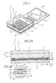
- the solid state imaging device 2 has a WLCSP structure and is constructed of a rectangular imaging chip 4 which is provided with image sensors 3 and an assembly substrate 5 on which the imaging chip 4 is assembled.
- the imaging chip 4 includes a semiconductor substrate 6 on whose upper face the image sensors 3 are formed, a frame-like spacer 7 which is attached onto the semiconductor substrate 6 so as to surround the image sensors 3, and a cover glass 8 as a translucent member or a translucent substrate.
- the cover glass 8 is disposed above the spacer 7 so as to tightly close the image sensors 3.
- the semiconductor substrate 6 is obtained by dividing a silicon wafer so as to have a rectangular shape, and has the image sensors 3 in a central area of an upper face and plural contact terminals 10 arranged on the confronting two edges.
- the thickness t of the semiconductor substrate 6 is decreased, for example in the range of 30 ⁇ m to 100 ⁇ m, and preferably to about 50 ⁇ m, which is effective for decreasing the thickness of the solid state imaging device 2. Further, when the semiconductor substrate 6 becomes thinner, the length of wires becomes shorter. Accordingly, the responding speed of the solid state imaging device becomes higher.
- the image sensors 3 are, for example, constructed of plural pixels arranged in matrix form, a charge coupled device (CCD) for transporting an electric charge accumulated in the pixels.
- CCD charge coupled device
- a micro lens or RGB color filters are superimposed on each pixels.
- Each contact terminal 10 is formed of aluminum and positioned on an upper face of the semiconductor substrate 6 so as to electrically connect the image sensors 3.
- the cover glass 8 is constructed of a low- ⁇ -ray glass 12, and an IR-cut filter 13 which is joined on the low- ⁇ -ray glass 12.
- the low- ⁇ -ray glass 12 is a glass from which only a small intensity of ⁇ -ray is generated, so as to prevent that the pixels of the image sensors 3 is destroyed by the ⁇ -ray.
- the IR-cut filter 13 cuts the infrared ray in the predetermined wavelength range so as to prevent a ghost and fogging. On the IR-cut filter is superimposed a low-path filter for preventing the occurance of false color. Since the low- ⁇ -ray glass 12 and the IR-cut filter 13 are integrated, the attachment space becomes smaller and the attachment operations become easier.
- the spacer 7 has an opening 15 in the center to have a frame-like shape, and is adhered onto the upper face of the semiconductor substrate 6 with an adhesive agent 16 so as to surround the image sensors 3.
- the spacer 7 is formed of inorganic materials whose coefficient of thermal expansion is closed to that of the semiconductor substrate 6, for example, silicon, stainless and the like.
- the disposition of the spacer 7 forms a space between the image sensors 3 and the cover glass 8. Since the space prevents the interference of the cover glass 8 to a micro lens of the image sensors 3, the functions of the micro lens don't become worse. Further, since the spacer 7 can seal the contact terminals 10 all together, the width of sealing can be larger than when only the image sensors 3 is sealed. Thus the effects of sealing becomes higher.
- the through-hole 18 has a nearly corn like shape such that the diameter of the top may be ⁇ 0.1mm, and that of the bottom may be ⁇ 0.12mm.
- the assembly substrate 5 is constructed of a flexible printed circuit board 21 and a reinforcement plate 22.
- an interconnection circuit pattern 20 is formed on the flexible printed circuit board 21 as a pattern of a periphery circuitry.
- the imaging chips 4 are assembled and reinforced by the reinforcement plate 22.
- a diebond of the imaging chips 4 on the assembling substrate 5 is made with an insulating adhesive agent (or non-conductive resin paste) 23 applied to the flexible printed circuit board 21, and an IC 24 (for example DSP) and the like are assembled on the flexible printed circuit board 21 in which several sorts of circuits for driving the imaging chips 4 are incorporated
- bumps there are formed plural stud bumps (hereinafter, bumps) on the interconnection circuit pattern 20 on the upper surface of the flexible printed circuit board 21.
- Each bump is formed of gold (Au) and has a diameter of ⁇ 0.06mm and a height of 0.08mm.
- the bump 26 is used for forming the connect terminal in a side of the bottom instead of using through-hole interconnections, and therefore many processes of high cost that are necessary for forming the through-hole interconnections are omitted. Further, the defective interconnection caused by the voids in the through-hole interconnections is prevented, and therefore it is prevented that the image quality of the solid state imaging device 2 becomes lower.
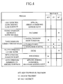
- a producing method of the solid state imaging device 2 will be explained with reference to FIG.4 as a table in which operation steps in the producing process of the solid state imaging device 2, concrete works in each operation, and treatments of each work are described.
- the treatments there are a high-temperature treatment performed under the high temperature, a vacuum treatment performed in vacuum, and a wet treatment performed with use of liquid. The performed treatment checked and marked with an asterisk.
- the joining the wafer and the glass substrate is made.
- the wafer 30 is obtained by forming many image sensors 3 and the contact terminals 10 on a well-known silicone wafer.
- the wafer 30 may be a standard wafer which is cheap and widely distributed.
- the standard wafer has a diameter of ⁇ 6 inch and a thickness of 625 ⁇ m.
- the glass substrate 32 includes a low- ⁇ -ray glass substrate 33 as a substrate for the low- ⁇ -ray glass 12, a filter substrate 34 as a substrate for the IR-cut filter 13 and a spacer 38 as a substrate of the spacer 7.
- the glass substrate 32 is produced in another line than the production line for the solid state imaging device 2, and supplied into the production line for the solid state imaging device 2.
- the low- ⁇ -ray glass substrate 33 and the filter substrate 34 are joined at first.
- an UV-adhesive agent 36 is applied to the low- ⁇ -ray glass substrate 33 with a constant thickness, the filter substrate 34 is superimposed thereon, and the vacuum pressing is made to tightly adhere the both.
- an UV-lay is irradiated to the UV-adhesive agent 36 through the filter substrate 34 to make the hardening.
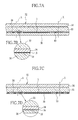
- the double dashed lines X in the FIGs.6A&6C illustrate positions for cutting the joined wafer 30 and the glass substrate 32 into the image sensors 3.
- the spacer 38 is joined with the adhesive agent 40 to a lower face of the low- ⁇ -ray glass substrate 33.
- a resist mask having the same shape as the spacer 7 is formed by the photolithography.
- a plasma etching is made such that many openings may be formed. After the etching, the resist mask is removed by an ashing and the like.
- the glass substrate 32 is superimposed on the wafer 30 and joined with the adhesive agent 16 applied to the spacer 38.
- alignment adhering device is used.
- the alignment adhering device makes the positioning adjustment between the wafer 30 and the glass substrate 32 in the X-Y directions while orientation flats 30a,32a are the standards thereby, and the pressure is applied so as to adhere the wafer 30 and the glass substrate 32 adequately. Since the imaging elements on the wafer 30 are sealed by the joint of the spacer 38 and the glass substrate 32, the dusts generated in the following operations does not adhere to the image sensors 3.
- the adhesive agent 16 used for joining the wafer 30 and the glass substrate 32 is, for example, a visible light delayed curing adhesive and the like in order to prevent the warpage in the hardening. Further, in order to form the adhesive layer whose thickness is thin and constant about several micrometers, the adhesive agent having the low viscosity is used.
- the wafer is made thinner.
- the wafer 30 is adhered to a protective tape such that scratches may not formed on the glass plate 32 which is joined on the upper face of the wafer.
- the wafer 30 is set to a backgrind device for grinding the bottom of the wafer.
- the water is sourced over the wafer 30 in order to prevent the temperature increase.
- the polishing is performed so as to make the surface of the wafer 30 flat.
- the thickness of the wafer 30 is decreased from 625 ⁇ m to the range of 30 - 100 ⁇ m, and preferably to 50 ⁇ m.
- the thickness of the solid state imaging device 2 can become smaller. Further, the grinding and polishing are performed to the single body of the wafer 30 before the joining, the strength thereof becomes lower, and therefore the handling and the like become more difficult. However, when the grinding and polishing is made after the joining to the glass substrate 32, the glass substrate 32 reinforces the wafer. Accordingly the handling characteristics of the wafer 30 don't become worse.
- the through-holes 18 are formed in the wafer 30 in the third operation.
- the resist mask is formed by the photolithography on the bottom of the wafer 30 except of the positions where the through-holes 18 are formed.
- the formation of the resist mask is performed by the wet treatment in which the developing liquids and the like are used.
- the plasma etching is made from the bottom side of the wafer 30, and part of the wafer that is not coated with the resist mask is removed.
- the plasma etching is performed under the vacuum circumstance.
- the resist mask is removed by the ashing which is performed in the vacuum condition or the high temperature condition.
- the formation of the through-hole 18 is completed in a short time since the thickness of the wafer 30 is made smaller in the previous process, and therefore the workability is increased. Further, the plasma etching is completed in a short time, the generation of the side etch is prevented.
- the wafer 30 joined with the glass substrate 32 is cut into the image sensors 3 on the double dashed line X in the fourth operation.
- the wafer 30 is set to a dicing device.
- the dicing device cools the wafer with sourcing water, and divides the joined wafer 30 and glass substrate 32 with use of metal resin grind stone which is made from coagulating diamond grinding sands with resin.
- metal resin grind stone which is made from coagulating diamond grinding sands with resin.
- the thickness decrease by the backgrind device and the cut by the dicing device are made with high accuracy. Accordingly, the movement accuracy of the image sensors 3 to the outer shape of the imaging chip 4, the positional accuracies in the XYZ directions are extremely high. Further, the bottom and the side face of the imaging chip 4 can be used enough as a standard face of the positioning even without additional processing. Thus the imaging chip 4 can be assembled into a camera module and the like based on the outer shape of the imaging chip 4, and the adjusting operation (such as the position adjustment) which takes long time can be omitted.
- bumps 26 are formed on the interconnection circuit pattern 20 of the flexible printed circuit board 21 in the fifth operation.
- the bump 26 is formed in the following steps. At first, a gold wire as the raw materials of the bump 26 is supplied by a wire bonder, and the electric discharge with high voltage is made to the gold wire in the moment. Thus the gold wire is melt and solidified in this moment to form a gold ball on the top of the gold wire. The gold ball is disposed on the interconnection circuit pattern 20, and then melt by the supersonic wave adhesion. At last the gold wire is broken to form the bump 26.
- the imaging chip 4 is assembled onto the assembly substrate 5 in the sixth operation.
- a non conductive resin paste (or NCP) 23 is applied onto the flexible printed circuit board 21, and then the imaging chip 4 is disposed on the flexible printed circuit board 21.
- Each bump 26 is inserted into the through-hole 18 to contact to the contact terminal 10.
- the non-conductive resin paste 23 is solidified by heat, such that the assembly of the imaging chip 4 on the assembly substrate 5 is completed.
- the solid state imaging device 2 is obtained.
- the producing method of the solid state imaging device since the through-hole interconnection is not formed, the many operations of the etching are omitted. Further, since the wafer to which the etching is performed has the smaller thickness, the time for the etching becomes one sixth shorter than the prior art. Further, the number of the steps in all of the vacuum treatment, the high-temperature treatment and the wet treatment is one third fewer than the prior art. Thus in the producing method of the solid state imaging device in the present invention, the production process (or the production cost) of the solid state imaging device 2 is one fourth decreased than the prior art.
- the imaging chip 4 is assembled on the assembly substrate 5.
- the interconnection circuit pattern may be formed on the bottom of the chip to be provided with a peripheral circuitry. Note that the detailed explanation for the same parts as the above embodiment is omitted.
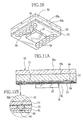
- a solid state imaging device 50 includes a semiconductor substrate 53, a frame-like spacer 54, cover glasses 55a,55b, a connection terminal 56, and an interconnection circuit pattern 58.
- On the semiconductor substrate 53 are formed plural imaging elements 51 and plural contact terminals 52.
- the frame-like spacer 54 is attached onto the semiconductor substrate 53 so as to surround the imaging elements 51, and the cover glasses 55a,55b are disposed above the spacer 54 so as to seal the imaging elements 51.
- Below the interconnection circuit pattern 58 is assembled an IC 57 in which several sorts of circuits for driving the image sensor 51 are incorporated.
- Through-holes 59 of nearly corn-like shape are formed on a lower face side of the semiconductor substrate 53 at the positions to confront the corresponding contact terminals 52. Through each through-hole 59, the contact terminal 52 appears on the lower face of the semiconductor substrate 53.
- bumps 60 which are made of gold so as to project toward below.
- the bottom of the semiconductor substrate 53 is covered with an insulation layer 61 formed of the insulation adhesive agent, and an end of the bump 60 protrudes from the insulation layer 61.
- a lower face of the insulation layer 61 is provided with the connection terminal 56 and the interconnection circuit pattern 58, and the connection terminal 58 is electrically connected to the bump 60.
- the IC 57 attached to the interconnection circuit pattern 56 is connected to the imaging elements 51.
- the producing method of the solid state imaging device 50 will be explained in reference with a table of FIG.12. Note that since the first to third operations are the same as in the above described producing method of the solid state imaging device 2, the explanation thereof is omitted.
- the bump 60 is formed in the through-hole 59 of a wafer 65 in the fourth operation.
- the insulation adhesive agent is applied to the bottom of the wafer 65 and solidified to form the insulation layer 61 in the fifth operation. Further, the grinding and the polishing of the bottom side of the wafer is made by the backgrind device, such that an end of the bump 60 may protrude from the insulation layer 61.
- the interconnection circuit pattern 58 and the connection terminal 56 are formed on the bottom of the insulation layer 61 in the sixth operation.
- the formation thereof is made in the steps of forming a resist mask by a photolithography, plating in a liquid in which the bottom side of the semiconductor substrate 53 is dipped into the liquid, and removing the mask.
- the dicing of the joined wafer 65 and glass substrates 67a, 67b is made, and thus the plurality of the solid state imaging device 50 is completely produced.
- On the bottom of each solid state imaging device 50 is attached the IC 57.
- the solid state imaging device 50 since the through-hole interconnections are not used, the problems caused by the through-hole interconnections are solved similarly to the solid state imaging device 2 shown in FIG.1. Further, a peripheral circuitry can be formed on the bottom of the semiconductor substrate 53, the assembly size of the solid state imaging device 50 is made smaller. Furthermore, the thickness t of the semiconductor substrate 53 is decreased to the range of 30 ⁇ m to 100 ⁇ m, and preferably to about 50 ⁇ m the same as that of the solid state imaging device 2 shown in FIG.1. Therefore even when the IC 57 is formed on the bottom, the imaging apparatus 50 does not become extremely thick.
- the time for performing the etching is one fifth shorter than the solid state imaging device of the prior art. Furthermore, the number of the steps in all of the vacuum treatment, the high-temperature treatment and the wet treatment is reduced to half than the prior art. Thus in the producing method of the solid state imaging device in the present invention, the production process (or the production cost) of the solid state imaging device 2 is decreased to half of that in the prior art.
- the bump 26 is formed on the assembly substrate 5.
- the bump may be formed in the through-hole 18 of the semiconductor substrate 6.
- the through-holes are formed in the semiconductor substrate such that the connection terminal may expose.
- the through-holes may be formed in the cover glass such that the connect terminal may be exposed on upper face of the solid state imaging device.
- all over the upper face of the semiconductor substrate is sealed by the cover glass.
- the present invention can be applied to the solid state imaging device in which only a space on the imaging sensors may be sealed by the cover glass and the contact terminal on the semiconductor substrate is exposed.
- the CCD is used as the solid state imaging device.
- the present invention can be applied to the solid state imaging device of the CMOS type.
- an example of the solid state imaging device is the WLCSP type.
- the present invention can be applied to the solid state imaging device of the CSP type or bare chip assembly type. Further, the present invention can be applied to a semiconductor device other than the solid state imaging device.
Landscapes
- Solid State Image Pick-Up Elements (AREA)
Abstract
Description
Claims (20)
- A solid state imaging device (2, 50) comprising:a semiconductor substrate (6, 53) having a first face and a second face, in said first face being formed image sensors (3, 51) and plural contact terminals (10, 52) connected to said respective image sensors (3, 51), said each contact terminal appearing on said second face through said through-hole (18, 59) formed by piercing said semiconductor substrate (6, 53) from a side of said second face;a translucent member (8, 12, 13, 55a, 55b) superimposed on said first face of said semiconductor substrate (6, 53) so as to seal said image sensors (3, 51) and said contact terminals (10, 52);an assembly substrate (5) for assembling said semiconductor substrate (6, 53) thereon; andplural bumps (26, 60) formed in at least one of said semiconductor substrate (6, 53) and said assembly substrate (5), so as to connect said contact terminal (10, 52) in said each through-hole (18, 59) to said assembly substrate (5).
- A solid state imaging device (2, 50) as described in claim 1, wherein a space is formed between said image sensors (3, 51) and said translucent member (8, 12, 13, 55a, 55b).
- A solid state imaging device (2, 50) as described in claim 1, wherein said translucent member (8, 12, 13, 55a, 55b) is one of a low-α-ray glass (12), IR-cut filter (13) and a low path filter.
- A solid state imaging device (2, 50) as described in claim 1, further comprising a spacer (7, 38) disposed between said translucent member (8, 12, 13, 55a, 55b) and said semiconductor substrate (6, 53).
- A solid state imaging device (2, 50) as described in claim 4, wherein a raw material of said spacer (7, 38) is one of stainless and silicon.
- A solid state imaging device (2, 50) as described in claim 1, wherein said semiconductor substrate (6, 53) is from 30 to 100µm in thickness.
- A solid state imaging device (2, 50) comprising:a semiconductor substrate (6, 53) having a first face and a second face, in said first face being formed image sensors (3, 51) and plural contact terminals (10, 52) connected to said respective image sensors (3, 51), said each contact terminal (10, 52) appearing on said second face through said through-hole (18, 59) formed by piercing said semiconductor substrate (6, 53) from a side of said second face;a translucent member (8, 12, 13, 55a, 55b) superimposed on said first face of said semiconductor substrate (6, 53) so as to seal said image sensors (3, 51) and said contact terminals (10, 52);a connection terminal (56) formed on said second face of said semiconductor substrate (6, 53); andplural bumps (26, 60) formed in said respective through-holes (18, 59), so as to connect said contact terminal (10, 52) in said each through-hole (18, 59) and said connection terminal (56).
- A solid state imaging device (2, 50) as described in claim 7, further comprising a pattern (20, 58) of peripheral circuitry formed on said second face, on said pattern (20, 58) being assembled electric parts for said peripheral circuitry.
- A solid state imaging device (2, 50) as described in claim 7, wherein a space is formed between said image sensors (3, 51) and said translucent member (8, 12, 13, 55a, 55b).
- A solid state imaging device (2, 50) as described in claim 7, wherein said translucent member (8, 12, 13, 55a, 55b) is one of a low-α-ray glass, IR-cut filter and a low path filter.
- A solid state imaging device (2, 50) as described in claim 7, further comprising a spacer (7, 38) disposed between said translucent member (8, 12, 13, 55a, 55b) and said semiconductor substrate (6, 53).
- A solid state imaging device (2, 50) as described in claim 11, wherein a raw material of said spacer (7, 38) is one of stainless and silicon.
- A solid state imaging device (2, 50) as described in claim 7, wherein said semiconductor substrate (6, 53) is from 30 to 100µm in thickness.
- A producing method of said solid state imaging device (2, 50), comprising steps of:forming on a first face of a wafer (30, 65) plural units constructed of plural image sensors (3, 51) and plural contact terminals (10, 52) respectively connected to said image sensors (3, 51);joining a translucent substrate (32, 33, 34, 67) onto said first face of said wafer (30, 65) to seal said image sensor (3, 51) and said contact terminals (10, 52);forming plural through-holes (18, 59) in said wafer (30, 65) from a side of said second face, such that said plural contact terminals (10, 52) may appear on a second face;cutting said joined wafer (30, 65) and translucent substrate (32, 33, 34, 67) at each of said units such that plural semiconductor substrate (6, 53)s may be obtained;forming bumps (26, 60) on an assembly substrate (5); andassembling said semiconductor substrate (6, 53) on said assembly substrate (5), so as to connect said contact terminal (10, 52) in said each through-hole (18, 59) to said assembly substrate (5) through said bump (26, 60).
- A producing method as described in claim 14, wherein said second face is ground before forming said though-holes.
- A producing method as described in claim 15, wherein said grinding is made such that a thickness of said wafer (30, 65) may be in the range of 30µm to 100µm.
- A producing method of said solid state imaging device (2, 50), comprising steps of:forming on a first face of a wafer (30, 65) plural units constructed of plural image sensors (3, 51) and plural contact terminals (10, 52) respectively connected to said image sensors (3, 51);joining a translucent substrate (32, 33, 34, 67) onto said first face of said wafer (30, 65) to seal said image sensor (3, 51) and said contact terminals (10, 52);forming plural through-holes (18, 59) in said wafer (30, 65) from a side of said second face, such that said plural contact terminals (10, 52) may appear on a second face;forming bumps (26, 60) in said respective through-holes (18, 59);forming plural connection terminal (56) s on said second face of said wafer (30, 65) so as to connect said connection terminal (56) and said contact terminals (10, 52) through said bumps (26, 60); andcutting said joined wafer (30, 65) and translucent substrate (32, 33, 34, 67) for each of said unit.
- A producing method as described in claim 17, further comprising steps of:forming a pattern (20, 58) of a peripheral circuitry on said second face of said wafer (30, 65); andassembling electric parts for said peripheral circuitry on said pattern (20, 58).
- A producing method as described in claim 18, wherein said second face of said wafer (30, 65) is ground before forming said through-holes (18, 59).
- A producing method as described in claim 19, wherein said grinding is made such that a thickness of said wafer (30, 65) may be in the range of 30µm to 100µm.
Applications Claiming Priority (2)
| Application Number | Priority Date | Filing Date | Title |
|---|---|---|---|
| JP2003394221A JP4542768B2 (en) | 2003-11-25 | 2003-11-25 | Solid-state imaging device and manufacturing method thereof |
| JP2003394221 | 2003-11-25 |
Publications (2)
| Publication Number | Publication Date |
|---|---|
| EP1536478A2 true EP1536478A2 (en) | 2005-06-01 |
| EP1536478A3 EP1536478A3 (en) | 2008-07-23 |
Family
ID=34463779
Family Applications (1)
| Application Number | Title | Priority Date | Filing Date |
|---|---|---|---|
| EP04257300A Withdrawn EP1536478A3 (en) | 2003-11-25 | 2004-11-24 | Solid state imaging device and producing method thereof |
Country Status (5)
| Country | Link |
|---|---|
| US (3) | US7259438B2 (en) |
| EP (1) | EP1536478A3 (en) |
| JP (1) | JP4542768B2 (en) |
| KR (1) | KR100684703B1 (en) |
| CN (1) | CN1622334B (en) |
Cited By (6)
| Publication number | Priority date | Publication date | Assignee | Title |
|---|---|---|---|---|
| EP1973166A3 (en) * | 2007-03-21 | 2011-05-04 | EM Microelectronic-Marin SA | Photoreceptor integrated circuit and optoelectronic component comprising the photoreceptor integrated circuit |
| US7939361B2 (en) | 2006-09-15 | 2011-05-10 | Fujitsu Semiconductor Limited | Semiconductor device and method for fabricating semiconductor device |
| US8053852B2 (en) | 2005-02-17 | 2011-11-08 | Semiconductor Components Industries, Llc | Light sensor receiving light from backside |
| FR2968832A1 (en) * | 2010-12-08 | 2012-06-15 | St Microelectronics Grenoble 2 | METHOD FOR MANUFACTURING SEMICONDUCTOR DEVICES AND SEMICONDUCTOR DEVICES |
| US11410896B2 (en) | 2016-02-08 | 2022-08-09 | Sony Corporation | Glass interposer module, imaging device, and electronic apparatus |
| EP4447472A1 (en) * | 2023-04-11 | 2024-10-16 | STMicroelectronics International N.V. | Stacked filter assembly for optical integrated circuit package with an optical filter mounted to an optical integrated circuit device by a discrete semiconductor spacer block |
Families Citing this family (27)
| Publication number | Priority date | Publication date | Assignee | Title |
|---|---|---|---|---|
| JP4000507B2 (en) | 2001-10-04 | 2007-10-31 | ソニー株式会社 | Method for manufacturing solid-state imaging device |
| JP2006228837A (en) * | 2005-02-15 | 2006-08-31 | Sharp Corp | Semiconductor device and manufacturing method thereof |
| TW200644261A (en) * | 2005-06-06 | 2006-12-16 | Megica Corp | Chip-package structure and manufacturing process thereof |
| US7288757B2 (en) | 2005-09-01 | 2007-10-30 | Micron Technology, Inc. | Microelectronic imaging devices and associated methods for attaching transmissive elements |
| KR100738653B1 (en) * | 2005-09-02 | 2007-07-11 | 한국과학기술원 | Wafer Level Chip Size Package for Image Sensor Module and Its Manufacturing Method |
| US7417221B2 (en) * | 2005-09-08 | 2008-08-26 | Gentex Corporation | Automotive vehicle image sensor |
| JP4764710B2 (en) * | 2005-12-06 | 2011-09-07 | 株式会社ザイキューブ | Semiconductor device and manufacturing method thereof |
| JP2007188909A (en) * | 2005-12-14 | 2007-07-26 | Fujifilm Corp | Solid-state imaging device and manufacturing method thereof |
| JP2007180239A (en) * | 2005-12-27 | 2007-07-12 | Sharp Corp | Soldering mounting structure, manufacturing method and manufacturing apparatus, electronic device, and wiring board |
| JP2007208045A (en) * | 2006-02-02 | 2007-08-16 | Sony Corp | Imaging device, camera module, electronic device, and manufacturing method of imaging device |
| US20070236591A1 (en) * | 2006-04-11 | 2007-10-11 | Tam Samuel W | Method for mounting protective covers over image capture devices and devices manufactured thereby |
| JP2007294658A (en) * | 2006-04-25 | 2007-11-08 | Fujikura Ltd | Semiconductor package |
| US20080067330A1 (en) * | 2006-09-19 | 2008-03-20 | Denso Corporation | Color sensor for vehicle and method for manufacturing the same |
| US8456560B2 (en) * | 2007-01-26 | 2013-06-04 | Digitaloptics Corporation | Wafer level camera module and method of manufacture |
| WO2008133943A1 (en) | 2007-04-24 | 2008-11-06 | Flextronics Ap Llc | Small form factor modules using wafer level optics with bottom cavity and flip chip assembly |
| US20080265356A1 (en) * | 2007-04-27 | 2008-10-30 | Jin-Chyuan Biar | Chip size image sensing chip package |
| JP4890398B2 (en) * | 2007-09-19 | 2012-03-07 | パナソニック株式会社 | Imaging device |
| US20090121300A1 (en) * | 2007-11-14 | 2009-05-14 | Micron Technology, Inc. | Microelectronic imager packages and associated methods of packaging |
| JP5392458B2 (en) * | 2008-08-21 | 2014-01-22 | 株式会社ザイキューブ | Semiconductor image sensor |
| JP5510877B2 (en) * | 2008-10-07 | 2014-06-04 | 株式会社リコー | Sensor module and sensing device |
| JP5197436B2 (en) * | 2009-02-26 | 2013-05-15 | 株式会社東芝 | Sensor chip and manufacturing method thereof. |
| US9419032B2 (en) * | 2009-08-14 | 2016-08-16 | Nanchang O-Film Optoelectronics Technology Ltd | Wafer level camera module with molded housing and method of manufacturing |
| JP5721370B2 (en) * | 2010-08-27 | 2015-05-20 | キヤノン株式会社 | Manufacturing method of optical sensor, optical sensor and camera |
| JP5791461B2 (en) * | 2011-10-21 | 2015-10-07 | 浜松ホトニクス株式会社 | Photodetector |
| CN104284060B (en) * | 2013-07-12 | 2019-07-02 | 鸿富锦精密工业(深圳)有限公司 | camera module |
| WO2017010063A1 (en) * | 2015-07-10 | 2017-01-19 | 凸版印刷株式会社 | Wiring substrate and method for manufacturing same |
| JP6745418B2 (en) | 2018-01-29 | 2020-08-26 | 富士フイルム株式会社 | Imaging unit and imaging device |
Family Cites Families (16)
| Publication number | Priority date | Publication date | Assignee | Title |
|---|---|---|---|---|
| JPH085566Y2 (en) * | 1989-07-12 | 1996-02-14 | オリンパス光学工業株式会社 | Solid-state imaging device |
| JPH085566A (en) | 1994-06-20 | 1996-01-12 | Matsushita Electric Ind Co Ltd | Inspection method for foreign matter and defects of optical parts |
| JP2000195861A (en) * | 1998-12-25 | 2000-07-14 | Texas Instr Japan Ltd | Semiconductor device and manufacturing method thereof |
| JP3589421B2 (en) * | 1999-06-30 | 2004-11-17 | Hoya株式会社 | Window material glass for semiconductor package and method of manufacturing the same |
| JP3638229B2 (en) * | 1999-07-02 | 2005-04-13 | ペンタックス株式会社 | Interchangeable camera back SLR camera |
| US6389687B1 (en) * | 1999-12-08 | 2002-05-21 | Amkor Technology, Inc. | Method of fabricating image sensor packages in an array |
| JP3527166B2 (en) * | 2000-03-15 | 2004-05-17 | シャープ株式会社 | Solid-state imaging device and method of manufacturing the same |
| US6384472B1 (en) * | 2000-03-24 | 2002-05-07 | Siliconware Precision Industries Co., Ltd | Leadless image sensor package structure and method for making the same |
| JP2001351997A (en) * | 2000-06-09 | 2001-12-21 | Canon Inc | Mounting structure of light receiving sensor and method of using the same |
| JP2002368235A (en) * | 2001-03-21 | 2002-12-20 | Canon Inc | Semiconductor device and manufacturing method thereof |
| JP3839271B2 (en) * | 2001-05-01 | 2006-11-01 | 富士写真フイルム株式会社 | Solid-state imaging device and manufacturing method thereof |
| US6613597B2 (en) * | 2001-06-29 | 2003-09-02 | Xanoptix, Inc. | Optical chip packaging via through hole |
| JP4000507B2 (en) * | 2001-10-04 | 2007-10-31 | ソニー株式会社 | Method for manufacturing solid-state imaging device |
| EP1453097A4 (en) * | 2001-11-05 | 2008-01-23 | Zycube Co Ltd | SEMICONDUCTOR IMAGE SENSOR AND METHOD FOR MANUFACTURING THE SAME |
| JP4237966B2 (en) * | 2002-03-08 | 2009-03-11 | 浜松ホトニクス株式会社 | Detector |
| JP4443865B2 (en) * | 2002-06-24 | 2010-03-31 | 富士フイルム株式会社 | Solid-state imaging device and manufacturing method thereof |
-
2003
- 2003-11-25 JP JP2003394221A patent/JP4542768B2/en not_active Expired - Fee Related
-
2004
- 2004-11-22 US US10/992,776 patent/US7259438B2/en not_active Expired - Fee Related
- 2004-11-24 EP EP04257300A patent/EP1536478A3/en not_active Withdrawn
- 2004-11-24 KR KR1020040096743A patent/KR100684703B1/en not_active Expired - Fee Related
- 2004-11-25 CN CN2004100955127A patent/CN1622334B/en not_active Expired - Fee Related
-
2006
- 2006-02-07 US US11/348,308 patent/US7527990B2/en not_active Expired - Fee Related
-
2007
- 2007-04-20 US US11/785,839 patent/US7345349B2/en not_active Expired - Fee Related
Cited By (7)
| Publication number | Priority date | Publication date | Assignee | Title |
|---|---|---|---|---|
| US8053852B2 (en) | 2005-02-17 | 2011-11-08 | Semiconductor Components Industries, Llc | Light sensor receiving light from backside |
| US7939361B2 (en) | 2006-09-15 | 2011-05-10 | Fujitsu Semiconductor Limited | Semiconductor device and method for fabricating semiconductor device |
| EP1973166A3 (en) * | 2007-03-21 | 2011-05-04 | EM Microelectronic-Marin SA | Photoreceptor integrated circuit and optoelectronic component comprising the photoreceptor integrated circuit |
| FR2968832A1 (en) * | 2010-12-08 | 2012-06-15 | St Microelectronics Grenoble 2 | METHOD FOR MANUFACTURING SEMICONDUCTOR DEVICES AND SEMICONDUCTOR DEVICES |
| EP2463909A3 (en) * | 2010-12-08 | 2013-10-30 | STMicroelectronics (Grenoble 2) SAS | Method for manufacturing semiconductor devices and semiconductor devices |
| US11410896B2 (en) | 2016-02-08 | 2022-08-09 | Sony Corporation | Glass interposer module, imaging device, and electronic apparatus |
| EP4447472A1 (en) * | 2023-04-11 | 2024-10-16 | STMicroelectronics International N.V. | Stacked filter assembly for optical integrated circuit package with an optical filter mounted to an optical integrated circuit device by a discrete semiconductor spacer block |
Also Published As
| Publication number | Publication date |
|---|---|
| US20070187791A1 (en) | 2007-08-16 |
| EP1536478A3 (en) | 2008-07-23 |
| US7345349B2 (en) | 2008-03-18 |
| KR20050050562A (en) | 2005-05-31 |
| US7527990B2 (en) | 2009-05-05 |
| CN1622334B (en) | 2011-07-06 |
| CN1622334A (en) | 2005-06-01 |
| US7259438B2 (en) | 2007-08-21 |
| JP2005158948A (en) | 2005-06-16 |
| US20060128044A1 (en) | 2006-06-15 |
| US20050110107A1 (en) | 2005-05-26 |
| JP4542768B2 (en) | 2010-09-15 |
| KR100684703B1 (en) | 2007-02-20 |
Similar Documents
| Publication | Publication Date | Title |
|---|---|---|
| US7345349B2 (en) | Solid state imaging device and producing method thereof | |
| US8012776B2 (en) | Methods of manufacturing imaging device packages | |
| US7510902B2 (en) | Image sensor chip package and method of fabricating the same | |
| JP3540281B2 (en) | Imaging device | |
| US7215015B2 (en) | Imaging system | |
| US6737292B2 (en) | Method of fabricating an image sensor module at the wafer level and mounting on circuit board | |
| JP3527166B2 (en) | Solid-state imaging device and method of manufacturing the same | |
| US20080251872A1 (en) | Image sensor package, method of manufacturing the same, and image sensor module including the image sensor package | |
| TWI263319B (en) | Method of making camera module in wafer level | |
| CN101632177A (en) | Packaging method for imager device | |
| CN101339951A (en) | Image sensor package using removable protective film and method thereof | |
| JP2002009265A (en) | Solid-state imaging device | |
| KR100747611B1 (en) | Microelement Package and Manufacturing Method Thereof | |
| CN101521185A (en) | Package structure and process for optical chip | |
| CN101010807A (en) | Method of making camera module in wafer level | |
| TWI242819B (en) | Method for manufacturing chip on glass type image sensor and structure of the same | |
| KR100756245B1 (en) | Camera module | |
| JP2004349369A (en) | Semiconductor package for solid-state imaging device and method of manufacturing the same | |
| TWI258210B (en) | Method for wafer level package of sensor chip | |
| JP2006245359A (en) | Photoelectric conversion device, and manufacturing method thereof | |
| JP2012090033A (en) | Imaging module | |
| KR20050008121A (en) | Solid-State Imaging Apparatus and Method For Manufacturing The Same |
Legal Events
| Date | Code | Title | Description |
|---|---|---|---|
| PUAI | Public reference made under article 153(3) epc to a published international application that has entered the european phase |
Free format text: ORIGINAL CODE: 0009012 |
|
| AK | Designated contracting states |
Kind code of ref document: A2 Designated state(s): AT BE BG CH CY CZ DE DK EE ES FI FR GB GR HU IE IS IT LI LU MC NL PL PT RO SE SI SK TR |
|
| AX | Request for extension of the european patent |
Extension state: AL HR LT LV MK YU |
|
| RAP1 | Party data changed (applicant data changed or rights of an application transferred) |
Owner name: FUJIFILM CORPORATION |
|
| PUAL | Search report despatched |
Free format text: ORIGINAL CODE: 0009013 |
|
| AK | Designated contracting states |
Kind code of ref document: A3 Designated state(s): AT BE BG CH CY CZ DE DK EE ES FI FR GB GR HU IE IS IT LI LU MC NL PL PT RO SE SI SK TR |
|
| AX | Request for extension of the european patent |
Extension state: AL HR LT LV MK YU |
|
| 17P | Request for examination filed |
Effective date: 20080828 |
|
| 17Q | First examination report despatched |
Effective date: 20081002 |
|
| AKX | Designation fees paid |
Designated state(s): DE FR GB |
|
| STAA | Information on the status of an ep patent application or granted ep patent |
Free format text: STATUS: THE APPLICATION IS DEEMED TO BE WITHDRAWN |
|
| 18D | Application deemed to be withdrawn |
Effective date: 20140603 |