EP1535364B1 - Dämpfungs- oder abschlusselement in koaxialbauweise für hochfrequente elektromagnetische wellen - Google Patents
Dämpfungs- oder abschlusselement in koaxialbauweise für hochfrequente elektromagnetische wellen Download PDFInfo
- Publication number
- EP1535364B1 EP1535364B1 EP03793557A EP03793557A EP1535364B1 EP 1535364 B1 EP1535364 B1 EP 1535364B1 EP 03793557 A EP03793557 A EP 03793557A EP 03793557 A EP03793557 A EP 03793557A EP 1535364 B1 EP1535364 B1 EP 1535364B1
- Authority
- EP
- European Patent Office
- Prior art keywords
- attenuation
- termination element
- plate
- shaped parts
- outer conductor
- Prior art date
- Legal status (The legal status is an assumption and is not a legal conclusion. Google has not performed a legal analysis and makes no representation as to the accuracy of the status listed.)
- Expired - Lifetime
Links
Images

Classifications
-
- H—ELECTRICITY
- H01—ELECTRIC ELEMENTS
- H01P—WAVEGUIDES; RESONATORS, LINES, OR OTHER DEVICES OF THE WAVEGUIDE TYPE
- H01P1/00—Auxiliary devices
- H01P1/22—Attenuating devices
- H01P1/225—Coaxial attenuators
-
- H—ELECTRICITY
- H01—ELECTRIC ELEMENTS
- H01P—WAVEGUIDES; RESONATORS, LINES, OR OTHER DEVICES OF THE WAVEGUIDE TYPE
- H01P1/00—Auxiliary devices
- H01P1/24—Terminating devices
- H01P1/26—Dissipative terminations
- H01P1/266—Coaxial terminations
Definitions
- the invention relates to a damping or termination element in Koaxialbauweise for high-frequency electromagnetic waves, with at least one resistance part, which is mounted in the outer conductor and has at least one electrical connection to an inner conductor part.
- damping elements have long been known.
- a difficulty with such a damping element is the dissipation of heat from the resistance part. Especially at high power levels, it can lead to high temperatures, which are undesirable.
- the cost of manufacturing is relatively high, especially when high precision is required. Another difficulty is the required length of the damping element for a desired damping.
- the generic US 2,689,294 discloses a damping element in coaxial design for electromagnetic waves.
- a resistance part is mounted in an outer conductor and has an electrical connection to an inner conductor part.
- the resistance part has platelet-shaped carrier, which are fastened between inner conductor part and outer conductor.
- the invention has for its object to provide a damping or terminating element of the type mentioned, which is cheaper, more compact, yet precise to produce.
- the resistance part consists of at least two rotated, plate-shaped parts which are each provided with a central slot and can be plugged together with them.
- circuits Prior to assembling the plate-like parts, circuits are inexpensively applied to them, for example by screen printing or photolithography.
- At least two plate-shaped parts are arranged in cross-section in a cross shape. This allows a damping element or termination with eight circuits. Since, as mentioned, the plate-shaped parts are preferably provided with the circuits before assembly, these eight circuits can be inexpensively applied, for example, by screen printing or photolithography.
- Such a cross-shaped arrangement enables a particularly favorable and precise mounting of the carrier in the interior of a cylindrical outer conductor. Since the heat can radiate on all sides, a high dissipation of heat from the resistance circuits is possible. At the same power, this results in lower surface temperatures. The life of the damping element can thus be extended. It is also advantageous that the coaxial structure in the region of the damping element or closing element is substantially retained and This results in fewer reflections than in a planar structure.
- At least one inner conductor part is slotted on the front side for receiving the resistance part, wherein the slotted region is formed in cross section corresponding to the cross section of the resistance part.
- the inner conductor part can then be attached to the carrier during manufacture and is preferably connected to conductive layers which are applied to the carriers. For example, if eight circuits are provided, the inner conductor can now be electrically connected directly to all these eight circuits, for example, plugged or soldered in this way.
- the plate-shaped parts are each inserted with an outer edge in each case a groove on the inside of the outer conductor. This allows a particularly accurate centering of the resistance part in the inner conductor. In these grooves also the plate-shaped parts can be connected by soldering to the outer conductor. However, this is not mandatory, since the plate-shaped parts are basically positively fixed in the grooves.
- the damping element is particularly suitable in metrology for the power protection of measuring heads or other measuring devices.
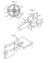
- damping element 1 is provided for high-frequency electromagnetic waves, for example, 40 GHz and is used for example in metrology for the protection of a meter. It is manufactured in coaxial design and has a hollow cylindrical outer conductor 2, which in an inner side 2a according to Fig. 2 has four grooves 6, in which a resistance part 3 is inserted.
- the resistance part 3 consists of at least two plate-shaped parts 4 and 5, each having a dielectric plate 4a and 5a, respectively, on which circuits 4b and 5b are applied on both sides.
- the dielectric plates 4 and 5 are made of, for example, ceramic or other suitable dielectic.
- the circuits 4b and 5b, and the in Fig. 3 concealed another six circuits are applied in a conventional manner, for example by screen printing or photolithography on dielectric plates 4 and 5.
- the plate-shaped parts 4 and 5 thus form so-called wafers, the production of which is known per se.
- the resistance part 3 is connected to two opposing inner conductor parts 7 and 8, which are bolt-shaped or pin-shaped and which are each provided at one end 7a and 8a with cross-shaped slots 8b. Through these slots 8b are according to Fig. 2 formed four symmetrically arranged fingers 8c, which engage in the resistance part 3. These fingers 8c are each connected to two conductor layers 9, in particular by means of solder joints 10.
- the connection of the inner conductor parts 7 and 8 to the resistance part 3 can also be done mechanically, for example by clamping.
- each inner conductor part 7 or 8 is connected to each of the eight circuits, in particular soldered. Each of the eight circuits thus has its own electrical contact.
- the resistance part 3 is according to the 3 and 4 assembled from two separately manufactured plate-shaped parts 4 and 5.
- the plate-like parts 4 and 5 consist, as explained above, of the dielectric plates 4a and 5a, the applied eight circuits, which in Fig. 4
- Each plate-shaped part 4 or 5 is also provided with a central slot 12 and 13, wherein the width of these slots 12 and 13 corresponds to the thickness of the plate-shaped parts 4 and 5, respectively.
- the plate-shaped parts 4 and 5 according to Fig. 4 put together in the direction of arrow 14.
- the slots 12 and 13 thus each take on the other part 4 and 5, respectively.
- the plate-shaped parts 4 and 5 can be slightly offset in the axial direction.
- an embodiment is conceivable in which more than two plate-shaped parts 4 and 5 are assembled.
- the conductor layers 9 and 19 serve for the connection of the inner conductor part 7. As already explained, the connection can be made by Lotstellen 10 or by mechanical clamping. In the arrangement according to Fig. 3 only one inner conductor part 7 is provided. Is a second inner conductor part 8 according to Fig. 1 provided, the plate-shaped parts 4 and 5 are provided in accordance with further conductor layers 9 and 19.
- the resistance part 3 is inserted into the inner conductor 2, wherein this is centered in the grooves 4 and precisely aligned.
- the resistance part 3 is connected in the grooves 6 with Lotstellen 11 with the outer conductor 2.
- the inner conductor 3 is thus connected at four points to the outer conductor 2, which allows the mentioned good heat dissipation.
- the resulting in the resistance part 3 heat can thus be derived in several directions in the outer conductor 2.
- the centering of the resistance part 3 in the four grooves 6 allows a comparatively large tolerance in the width of the electrical plates 4a and 5a. Since the plate-like parts 4 and 5 can be produced before assembly, the application of the circuits 4b and 5b in a conventional manner and inexpensively by screen printing or photolithography is possible.
- the production of the electrical platelets 4a and 5a is also possible cost-effectively, for example by cutting with a laser beam or by punching.
- end element 1 ' is essentially formed as the damping element 1, but has only only one inner conductor part and on the resistance part 3', the circuits 4a 'and 5b' and the circuits not visible here are guided according to the outside.
- the termination element 1 ' serves, for example, to prevent radiation or to eliminate impurities.
- Damping elements 1 can also be arranged one after the other in series, and after one or more damping elements 1, a terminating element 1 'can be connected.
- the heat output can be distributed over several elements.
Landscapes
- Non-Reversible Transmitting Devices (AREA)
- Waveguide Aerials (AREA)
- Communication Cables (AREA)
- Input Circuits Of Receivers And Coupling Of Receivers And Audio Equipment (AREA)
- Control Of Motors That Do Not Use Commutators (AREA)
Description
- Die Erfindung betrifft ein Dämpfungs- oder Abschlusselement in Koaxialbauweise für hochfrequent elektromagnetische Wellen, mit wenigstens einem Widerstandsteil, der im Aussenleiter gelagert und wenigstens einen elektrischen Anschluss an einen Innenleiterteil aufweist. Solche Dämpfungselemente sind seit langem bekannt. Beispielsweise zeigt die
US 3,227,975 , als nächstliegender Stand der Technik, ein Dämpfungselement zur nichteinstellbaren Abschwächung von elektromagnetischen Wellen, das einen dielektrischen plattenförmigen Träger aufweist, der in einem zylindrischen Aussenleiter angeordnet ist. Dieser dielektrische Träger befindet sich zwischen zwei Innenleiterenden. Auf dem Träger ist ein Film aus Widerstandsmaterial aufgetragen. Eine Schwierigkeit bei einem solchen Dämpfungselement ist die Ableitung der Wärme aus dem Widerstandsteil. Besonders bei hohen Leistungen kann es hier zu hohen Temperaturen kommen, welche unerwünscht sind. Zudem sind die Kosten für die Herstellung vergleichsweise hoch, insbesondere dann, wenn eine hohe Präzision gefordert ist. Eine weitere Schwierigkeit ist die benötigte Länge des Dämpfungselementes für eine erwünschte Dämpfung. - Die gattungsbildende
US 2,689,294 offenbart ein Dämpfungselement in Koaxialbauweise für elektromagnetische Wellen. Ein Widerstandsteil ist in einem Aussenleiter gelagert und weist einen elektrischen Anschluss an einen Innenleiterteil auf. Der Widerstandsteil weist plättchenförmige Träger auf, die zwischen Innenleiterteil und Aussenleiter befestigt sind. - Durch die
US 3,260,971 (Abbildung 7) ist ein Dämpfungselement bekannt geworden, bei welchem als Träger für den Widerstand ein einstückiger Teil vorgesehen ist, der im Querschnitt die Form eines Rades aufweist und eine walzenförmige Nabe besitzt, die ebenfalls einen Träger für Widerstandsbereiche bildet. Die Herstellung eines solchen Trägers und insbesondere das Aufbringen der Widerstände ist hier vergleichsweise aufwendig. Insbesondere ist es hier kaum möglich, die Widerstände mittels Siebdruck oder Photolithographie aufzubringen, wie dies in vielen Fällen wünschenswert und kostengünstig ist. - Der Erfindung liegt die Aufgabe zugrunde, ein Dämpfungs- oder Abschlusselement der genannten Art zu schaffen, das kostengünstiger, kompakter, und dennoch präzis herstellbar ist.
- Beim erfindungsgemässen Dämpfungs- oder Abschlusselement besteht der Widerstandsteil aus wenigstens zwei, gedreht liegenden, plättchenförmigen Teilen, die mit jeweils einem mittigen Schlitz versehen sind und mit diesen zusammensteckbar sind. Vor dem Zusammenbau der plättchenförmigen Teile werden auf diese beispielsweise mit Siebdruck oder Photolithographie kostengünstig Schaltungen aufgebracht.
- Nach einer Weiterbildung der Erfindung sind wenigstens zwei plättchenförmige Teile im Querschnitt kreuzförmig angeordnet. Dies ermöglicht ein Dämpfungselement oder einen Abschluss mit acht Schaltungen. Da wie erwähnt die plättchenförmigen Teile vorzugsweise vor dem Zusammenbau mit den Schaltungen versehen werden, können diese acht Schaltungen kostengünstig beispielsweise mit Siebdruck oder Photolithographie aufgebracht werden.
- Eine solche kreuzförmige Anordnung ermöglicht eine besonders günstige und präzise Lagerung des Trägers im Innern eines zylindrischen Aussenleiters. Da die Wärme nach allen Seiten abstrahlen kann, ist eine hohe Ableitung der Wärme aus den Widerstandsschaltungen möglich. Bei gleicher Leistung ergeben sich damit tiefere Oberflächentemperaturen. Die Lebensdauer des Dämpfungselementes kann damit verlängert werden. Vorteilhaft ist zudem, dass die koaxiale Struktur im Bereich des Dämpfungselementes bzw. Abschlusselements im Wesentlichen erhalten bleibt und dadurch weniger Reflexionen entstehen als bei einer planaren Struktur.
- Nach einer Weiterbildung der Erfindung ist wenigstens ein Innenleiterteil frontseitig zur Aufnahme des Widerstandsteils geschlitzt, wobei der geschlitzte Bereich im Querschnitt korrespondierend zum Querschnitt des Widerstandsteils ausgebildet ist. Der Innenleiterteil kann dann bei der Herstellung auf den Träger aufgesteckt werden und wird vorzugsweise mit leitenden Schichten verbunden, die auf die Träger aufgebracht sind. Sind beispielsweise acht Schaltungen vorgesehen, so kann nun auf diese Weise der Innenleiter mit allen diesen acht Schaltungen direkt elektrisch verbunden werden, beispielsweise gesteckt oder gelötet.
- Nach einer Weiterbildung der Erfindung sind die plättchenförmigen Teile jeweils mit einem äusseren Rand in jeweils eine Nut auf der Innenseite des Aussenleiters eingesetzt. Dies ermöglicht eine besonders genaue Zentrierung des Widerstandsteils im Innenleiter. In diesen Nuten können zudem die plättchenförmigen Teile durch Löten mit dem Aussenleiter verbunden werden. Dies ist jedoch nicht zwingend, da die plättchenförmigen Teile in den Nuten grundsätzlich formschlüssig fixierbar sind.
- Das Dämpfungselement eignet sich insbesondere in der Messtechnik für den Leistungsschutz von Messköpfen oder anderen Messvorrichtungen.
- Ausführungebeispiele der Erfindung werden nachfolgend anhand der Zeichnung näher erläutert. Es zeigen:
- Fig. 1 a
- schematisch eine Ansicht eines teilweise geschnittenen Dämpfungselementes,
- Fig. 1 b
- schematisch eine Ansicht eines teilweise geschnittenen Abschlusselementes,
- Fig. 2
- einen Schnitt durch das Dämpfungselement gemäss der Linie II-II der
Fig. 1a , - Fig. 3
- schematisch eine räumliche Ansicht eines Trägers mit acht Schaltungen und einem Innenleiterteil und
- Fig. 4
- schematisch das Fügen von zwei plättchenförmigen Teilen.
- Das in den
Fig. 1 und2 gezeigte Dämpfungselement 1 ist für hochfrequente elektromagnetische Wellen von beispielsweise 40 GHz vorgesehen und dient beispielsweise in der Messtechnik für den Schutz eines Messgerätes. Es ist in Koaxialbauweise hergestellt und weist einen hohlzylindrischen Aussenleiter 2 auf, der in einer Innenseite 2a gemässFig. 2 vier Nuten 6 aufweist, in die ein Widerstandsteil 3 eingesetzt ist. - Der Widerstandsteil 3 besteht aus wenigstens zwei plättchenförmigen Teilen 4 und 5, die jeweils ein dielektrisches Plättchen 4a bzw. 5a aufweisen, auf das beidseitig Schaltungen 4b bzw. 5b aufgebracht sind. Die dielektrischen Plättchen 4 und 5 bestehen beispielsweise aus Keramik oder einem anderen geeigneten Dielektikum. Die Schaltungen 4b und 5b, sowie die in
Fig. 3 verdeckten weiteren sechs Schaltungen sind in an sich bekannter Weise beispielsweise mit Siebdruck oder Photolithographie auf dielektrischen Plättchen 4 und 5 aufgebracht. Die plättchenförmigen Teile 4 und 5 bilden somit sogenannte Wafer, deren Herstellung an sich bekannt ist. - Der Widerstandsteil 3 ist an zwei gegenüber angeordneten Innenleiterteilen 7 und 8 angeschlossen, die bolzen- oder stiftförmig ausgebildet sind und die jeweils an einem Ende 7a bzw. 8a mit kreuzförmigen Schlitzen 8b versehen sind. Durch diese Schlitze 8b werden gemäss
Fig. 2 vier symmetrisch angeordnete Finger 8c gebildet, welche in den Widerstandsteil 3 eingreifen. Diese Finger 8c sind jeweils mit zwei Leiterschichten 9 verbunden, insbesondere mittels Lötstellen 10. Die Verbindung der Innenleiterteile 7 und 8 zum Widerstandsteil 3 kann auch mechanisch, beispielsweise durch Klemmung erfolgen. Wie ersichtlich, ist jeder Innenleiterteil 7 bzw. 8 mit jeder der acht Schaltungen verbunden, insbesondere verlötet. Jede der acht Schaltungen besitzt somit einen eigenen elektrischen Kontakt. - Der Widerstandsteil 3 wird gemäss den
Fig. 3 und 4 aus zwei separat hergestellten plättchenförmigen Teilen 4 und 5 zusammengebaut. Die plättchenförmigen Teile 4 und 5 bestehen, wie oben erläutert, aus den dielektrischen Plättchen 4a bzw. 5a, den aufgebrachten acht Schaltungen, die inFig. 4 nicht gezeigt sind, sowie Leiterschichten 9 bzw. 19. Jeder plättchenförmige Teil 4 bzw. 5 wird zudem mit einem mittigen Schlitz 12 bzw. 13 versehen, wobei die Breite dieser Schlitze 12 und 13 der Dicke der plättchenförmigen Teile 4 bzw. 5 entspricht. Für den Zusammenbau werden die plättchenförmigen Teile 4 und 5 gemässFig. 4 in Richtung des Pfeiles 14 zusammengesteckt. Die Schlitze 12 und 13 nehmen hierbei somit jeweils den anderen Teil 4 bzw. 5 auf. Sind die plättchenförmigen Teile 4 und 5 zusammengesteckt, so bilden sie die inFig. 3 gezeigte Anordnung, bei welcher die plättchenförmigen Teile 4 und 5 wie ersichtlich senkrecht aufeinander stehen. Grundsätzlich können die plättchenförmigen Teile 4 und 5 in Axialrichtung etwas versetzt sein. Zudem ist eine Ausführung denkbar, bei welcher mehr als zwei plättchenförmige Teile 4 und 5 zusammengebaut sind. - Die Leiterschichten 9 und 19 dienen für den Anschluss des Innenleiterteils 7. Wie bereits erläutert, kann die Verbindung durch Lotstellen 10 oder durch mechanische Klemmung erfolgen. Bei der Anordnung gemäss
Fig. 3 ist lediglich ein Innenleiterteil 7 vorgesehen. Ist ein zweiter Innenleiterteil 8 gemässFig. 1 vorgesehen, so werden die plättchenförmigen Teile 4 und 5 entsprechend mit weiteren Leiterschichten 9 und 19 versehen. - Der Widerstandsteil 3 wird in den Innenleiter 2 eingesetzt, wobei dieser in den Nuten 4 zentriert und präzise ausgerichtet wird. Vorzugsweise ist der Widerstandsteil 3 in den Nuten 6 mit Lotstellen 11 mit dem Aussenleiter 2 verbunden. Der Innenleiter 3 ist somit an vier Stellen mit dem Aussenleiter 2 verbunden, was die erwähnte gute Wärmeableitung ermöglicht. Die im Widerstandsteil 3 entstehende Wärme kann somit in mehreren Richtungen in den Aussenleiter 2 abgeleitet werden. Die Zentrierung des Widerstandsteils 3 in den vier Nuten 6 erlaubt eine vergleichsweise grosse Toleranz in der Breite der elektrischen Plättchen 4a und 5a. Da die plättchenförmigen Teile 4 und 5 vor dem Zusammenbau hergestellt werden können, ist das Aufbringen der Schaltungen 4b und 5b in an sich bekannter Weise und kostengünstig mit Siebdruck oder Photolithographie möglich. Die Herstellung der elektrischen Plättchen 4a und 5a ist ebenfalls kostengünstig beispielsweise durch Schneiden mit einem Laserstrahl oder durch Stanzen möglich.
- Das in der
Fig. 1b gezeigte Abschlusselement 1' ist im Wesentlichen wie das Dämpfungselement 1 ausgebildet, weist aber lediglich nur einen Innenleiterteil auf und auf dem Widerstandsteil 3' die Schaltungen 4a' und 5b' sowie die hier nicht sichtbaren Schaltungen sind entsprechend nach aussen geführt. Das Abschlusselement 1' dient beispielsweise zur Verhinderung von Abstrahlungen oder zur Elimination von Störstellen. - Dämpfungselemente 1 können auch in Serie nacheinander angeordnet sein und nach einem oder mehreren Dämpfungselementen 1 kann ein Abschlusselement 1' geschaltet sein. Die Wärmeabgabe kann so auf mehrere Elemente verteilt werden.
Claims (9)
- Dämpfungs- oder Abschlusselement in Koaxialbauweise für hochfrequente elektromagnetische Wellen, mit wenigstens einem Widerstandsteil (3, 3'), der wenigstens einen elektrischen Anschluss an einem Ende (7a, 8a) eines Innenleiterteils (7, 8) aufweist, und mit einem plättchenförmigen Teil (4, 5; 4', 5') der mit gegenüber liegenden, inneren Seiten des Aussenleiters (2) verbunden ist, dadurch gekennzeichnet, dass der Widerstandsteil wenigstens zwei, Kreuzförmig angeordnete, plättchenförmige Teile (4, 5; 4', 5') aufweist, die jeweils mit einem mittigen Schlitz (12, 13) versehen sind und mit diesen Schlitzen (12, 13) zusammensteckbar sind.
- Dämpfungs- oder Abschlusselement nach Anspruch 1, dadurch gekennzeichnet, dass wenigstens ein Innenleiterteil (7, 8) die beiden plättchenförmigen Teile (4, 5; 4', 5') fixiert.
- Dämpfungs- oder Abschlusselement nach Anspruch 1 oder 2, dadurch gekennzeichnet, dass die zwei plättchenförmigen Teile (4, 5; 4', 5') kreuzförmig zusammengesteckt sind.
- Dämpfungs- oder Abschlusselement nach einem der Ansprüche 1 bis 3, dadurch gekennzeichnet, dass die plättchenförmigen Teile (4, 5; 4', 5') jeweils beidseitig Schaltungen (4b, 5b; 4b', 5b') aufweisen, die insbesondere mittels Siebdruck oder Photolithographie auf dielektrischen Plättchen (4a, 5a; 4a', 5a') aufbringbar sind.
- Dämpfung- oder Abschlusselement nach Anspruch 4, dadurch gekennzeichnet, dass der Widerstandsteil (3, 3') wenigstens acht Schaltungen (4b, 5b; 4b', 5b') aufweist.
- Dämpfungs- oder Abschlusselement nach einem der Ansprüche 1 bis 5, dadurch gekennzeichnet, dass wenigstens ein Innenleiterteil (7, 8) an einem Ende (7a, 8a) geschlitzt ist, wobei der geschlitzte Bereich im Querschnitt korrespondierend zum Querschnitt des Widerstandsteils (3, 3') ausgebildet ist.
- Dämpfungs- oder Abschlusselement nach einem der Ansprüche 1 bis 6, dadurch gekennzeichnet, dass der Widerstandsteil (3, 3') in Nuten (6) der Innenseite (2a) des Aussenleiters (2) eingreift und in diesen Nuten (6) zentriert ist.
- Dämpfungs- oder Abschlusselement nach einem der Ansprüche 1 bis 7, dadurch gekennzeichnet, dass der Widerstandsteil (3, 3') auf der Innenseite des Aussenleiters (2) mittels eine Lötverbindung verbunden ist.
- Dämpfungselement nach einem der Ansprüche 1 bis 8, dadurch gekennzeichnet, dass es ein Teil oder Glied einer Messkette ist, insbesondere eine koaxiale Messkette.
Applications Claiming Priority (3)
| Application Number | Priority Date | Filing Date | Title |
|---|---|---|---|
| CH15072002 | 2002-09-04 | ||
| CH150702 | 2002-09-04 | ||
| PCT/CH2003/000590 WO2004023596A1 (de) | 2002-09-04 | 2003-08-29 | Dämpfungs- oder abschlusselement in koaxialbauweise für hochfrequente elektromagnetische wellen |
Publications (2)
| Publication Number | Publication Date |
|---|---|
| EP1535364A1 EP1535364A1 (de) | 2005-06-01 |
| EP1535364B1 true EP1535364B1 (de) | 2008-03-26 |
Family
ID=31954548
Family Applications (1)
| Application Number | Title | Priority Date | Filing Date |
|---|---|---|---|
| EP03793557A Expired - Lifetime EP1535364B1 (de) | 2002-09-04 | 2003-08-29 | Dämpfungs- oder abschlusselement in koaxialbauweise für hochfrequente elektromagnetische wellen |
Country Status (6)
| Country | Link |
|---|---|
| US (1) | US7212079B2 (de) |
| EP (1) | EP1535364B1 (de) |
| AT (1) | ATE390724T1 (de) |
| AU (1) | AU2003254692A1 (de) |
| DE (1) | DE50309484D1 (de) |
| WO (1) | WO2004023596A1 (de) |
Families Citing this family (5)
| Publication number | Priority date | Publication date | Assignee | Title |
|---|---|---|---|---|
| JP4456067B2 (ja) * | 2005-12-28 | 2010-04-28 | ヒロセ電機株式会社 | 高周波素子 |
| FR2918505B1 (fr) * | 2007-07-03 | 2011-04-01 | Radialla | Attenuateur coaxial |
| DE102010045780A1 (de) | 2010-09-17 | 2012-03-22 | Rohde & Schwarz Gmbh & Co. Kg | Kalibriereinheit für ein Messgerät |
| CN109786913B (zh) * | 2019-03-22 | 2023-09-01 | 西安雷航电子信息技术有限公司 | 一种基于薄膜电阻的射频同轴负载 |
| FR3146766A1 (fr) * | 2023-03-16 | 2024-09-20 | Radiall | Transition améliorée entre un contact central d’un composant coaxial et une ligne de transmission, notamment radiofréquence (RF). |
Family Cites Families (8)
| Publication number | Priority date | Publication date | Assignee | Title |
|---|---|---|---|---|
| GB606891A (en) * | 1944-06-14 | 1948-08-23 | Polytechnic Inst Brooklyn | Improvements relating to attenuators for electric waves |
| US2864063A (en) * | 1957-12-20 | 1958-12-09 | Polytechnic Inst Brooklyn | Microwave control devices |
| US3227975A (en) * | 1964-08-31 | 1966-01-04 | Hewlett Packard Co | Fixed coaxial line attenuator with dielectric-mounted resistive film |
| US3260971A (en) * | 1964-12-03 | 1966-07-12 | Weinschel Eng Co Inc | Multi-layer card attenuator for microwave frequencies |
| US4272739A (en) * | 1979-10-18 | 1981-06-09 | Morton Nesses | High-precision electrical signal attenuator structures |
| JPS61264801A (ja) | 1985-05-17 | 1986-11-22 | Mitsubishi Electric Corp | 円偏波発生器 |
| US5047737A (en) * | 1988-03-31 | 1991-09-10 | Wiltron Company | Directional coupler and termination for stripline and coaxial conductors |
| US5194834A (en) * | 1991-06-13 | 1993-03-16 | Semflex, Inc. | Apparatus for a matched and adjustable microwave frequency selective attenuator unit |
-
2003
- 2003-08-29 AT AT03793557T patent/ATE390724T1/de not_active IP Right Cessation
- 2003-08-29 US US10/526,292 patent/US7212079B2/en not_active Expired - Fee Related
- 2003-08-29 WO PCT/CH2003/000590 patent/WO2004023596A1/de not_active Ceased
- 2003-08-29 DE DE50309484T patent/DE50309484D1/de not_active Expired - Lifetime
- 2003-08-29 AU AU2003254692A patent/AU2003254692A1/en not_active Abandoned
- 2003-08-29 EP EP03793557A patent/EP1535364B1/de not_active Expired - Lifetime
Also Published As
| Publication number | Publication date |
|---|---|
| WO2004023596A1 (de) | 2004-03-18 |
| US7212079B2 (en) | 2007-05-01 |
| DE50309484D1 (de) | 2008-05-08 |
| HK1075134A1 (en) | 2005-12-02 |
| AU2003254692A1 (en) | 2004-03-29 |
| ATE390724T1 (de) | 2008-04-15 |
| EP1535364A1 (de) | 2005-06-01 |
| US20060097817A1 (en) | 2006-05-11 |
Similar Documents
| Publication | Publication Date | Title |
|---|---|---|
| DE3688588T2 (de) | Verkürzte Streifenleitungsantenne. | |
| DE102008005547B4 (de) | Leistungshalbleitermodul und Schaltungsanordnung mit einem Leistungshalbleitermodul | |
| DE68929198T2 (de) | Hochleistungsverbinder | |
| DE19707490C2 (de) | HF-Koaxial-Steckverbinder | |
| EP1941520B1 (de) | Widerstand, insbesondere smd-widerstand, und zugehöriges herstellungsverfahren | |
| DE3426565C2 (de) | ||
| DE102010044612A1 (de) | Elektrisch leitende Kontaktanordnung | |
| EP0892465A2 (de) | Leiterplatten-Nullkraftsteckverbinder | |
| DE69612054T2 (de) | Sicherungselement für träge Schmelzsicherung | |
| DE102011080468B4 (de) | Verfahren zur Herstellung eines Kontaktträgers eines Schaltkontaktes für ein elektromechanisches Schaltgerät sowie ein solcher Kontaktträger | |
| DE832022C (de) | Kristallkontaktvorrichtung und Verfahren zu ihrer Herstellung | |
| EP1449278A1 (de) | Stecker | |
| DE69813640T2 (de) | Elektrische verbinder | |
| EP1535364A1 (de) | Dämpfungs- oder abschlusselement in koaxialbauweise für hochfrequente elektromagnetische wellen | |
| DE2345583B2 (de) | Steckerleiste | |
| DE112007001472B4 (de) | Elektronikkomponentenmodul | |
| DE202009003687U1 (de) | Stützscheibe zum Abstützen von Hochfrequenz(HF)-Komponenten | |
| DE102004001899A1 (de) | Sperrkreisanordnung | |
| DE69422022T2 (de) | Antenneneinheit | |
| WO2008022632A1 (de) | Elektrisches bauelement, insbesondere messwiderstand sowie verfahren zur herstellung eines derartigen elektrischen bauelements | |
| DE19615497A1 (de) | Planarer Strahler | |
| EP1931187B1 (de) | Befestigungseinrichtung für elektronische Baugruppen sowie elektronisches Gerät mit einer derartigen Befestigungseinrichtung | |
| EP2932803B1 (de) | Kontaktanordnung für einen mehrlagigen schaltungsträger | |
| EP4293834A1 (de) | Elektrischer steckverbinder und elektrische steckverbindung | |
| EP4233124B1 (de) | Waffeleisen-filteranordnung für hochfrequenzsignale |
Legal Events
| Date | Code | Title | Description |
|---|---|---|---|
| PUAI | Public reference made under article 153(3) epc to a published international application that has entered the european phase |
Free format text: ORIGINAL CODE: 0009012 |
|
| 17P | Request for examination filed |
Effective date: 20050207 |
|
| AK | Designated contracting states |
Kind code of ref document: A1 Designated state(s): AT BE BG CH CY CZ DE DK EE ES FI FR GB GR HU IE IT LI LU MC NL PT RO SE SI SK TR |
|
| AX | Request for extension of the european patent |
Extension state: AL LT LV MK |
|
| REG | Reference to a national code |
Ref country code: HK Ref legal event code: DE Ref document number: 1075134 Country of ref document: HK |
|
| DAX | Request for extension of the european patent (deleted) | ||
| RIN1 | Information on inventor provided before grant (corrected) |
Inventor name: BLAVETTE, YANN |
|
| GRAP | Despatch of communication of intention to grant a patent |
Free format text: ORIGINAL CODE: EPIDOSNIGR1 |
|
| GRAS | Grant fee paid |
Free format text: ORIGINAL CODE: EPIDOSNIGR3 |
|
| GRAA | (expected) grant |
Free format text: ORIGINAL CODE: 0009210 |
|
| AK | Designated contracting states |
Kind code of ref document: B1 Designated state(s): AT BE BG CH CY CZ DE DK EE ES FI FR GB GR HU IE IT LI LU MC NL PT RO SE SI SK TR |
|
| REG | Reference to a national code |
Ref country code: GB Ref legal event code: FG4D Free format text: NOT ENGLISH |
|
| REG | Reference to a national code |
Ref country code: CH Ref legal event code: EP Ref country code: CH Ref legal event code: NV Representative=s name: ISLER & PEDRAZZINI AG Ref country code: IE Ref legal event code: FG4D Free format text: LANGUAGE OF EP DOCUMENT: GERMAN |
|
| REF | Corresponds to: |
Ref document number: 50309484 Country of ref document: DE Date of ref document: 20080508 Kind code of ref document: P |
|
| PG25 | Lapsed in a contracting state [announced via postgrant information from national office to epo] |
Ref country code: FI Free format text: LAPSE BECAUSE OF FAILURE TO SUBMIT A TRANSLATION OF THE DESCRIPTION OR TO PAY THE FEE WITHIN THE PRESCRIBED TIME-LIMIT Effective date: 20080326 |
|
| NLV1 | Nl: lapsed or annulled due to failure to fulfill the requirements of art. 29p and 29m of the patents act | ||
| PG25 | Lapsed in a contracting state [announced via postgrant information from national office to epo] |
Ref country code: SI Free format text: LAPSE BECAUSE OF FAILURE TO SUBMIT A TRANSLATION OF THE DESCRIPTION OR TO PAY THE FEE WITHIN THE PRESCRIBED TIME-LIMIT Effective date: 20080326 |
|
| REG | Reference to a national code |
Ref country code: IE Ref legal event code: FD4D |
|
| PG25 | Lapsed in a contracting state [announced via postgrant information from national office to epo] |
Ref country code: ES Free format text: LAPSE BECAUSE OF FAILURE TO SUBMIT A TRANSLATION OF THE DESCRIPTION OR TO PAY THE FEE WITHIN THE PRESCRIBED TIME-LIMIT Effective date: 20080707 Ref country code: CZ Free format text: LAPSE BECAUSE OF FAILURE TO SUBMIT A TRANSLATION OF THE DESCRIPTION OR TO PAY THE FEE WITHIN THE PRESCRIBED TIME-LIMIT Effective date: 20080326 Ref country code: SK Free format text: LAPSE BECAUSE OF FAILURE TO SUBMIT A TRANSLATION OF THE DESCRIPTION OR TO PAY THE FEE WITHIN THE PRESCRIBED TIME-LIMIT Effective date: 20080326 Ref country code: SE Free format text: LAPSE BECAUSE OF FAILURE TO SUBMIT A TRANSLATION OF THE DESCRIPTION OR TO PAY THE FEE WITHIN THE PRESCRIBED TIME-LIMIT Effective date: 20080626 Ref country code: PT Free format text: LAPSE BECAUSE OF FAILURE TO SUBMIT A TRANSLATION OF THE DESCRIPTION OR TO PAY THE FEE WITHIN THE PRESCRIBED TIME-LIMIT Effective date: 20080901 |
|
| PG25 | Lapsed in a contracting state [announced via postgrant information from national office to epo] |
Ref country code: NL Free format text: LAPSE BECAUSE OF FAILURE TO SUBMIT A TRANSLATION OF THE DESCRIPTION OR TO PAY THE FEE WITHIN THE PRESCRIBED TIME-LIMIT Effective date: 20080326 Ref country code: RO Free format text: LAPSE BECAUSE OF FAILURE TO SUBMIT A TRANSLATION OF THE DESCRIPTION OR TO PAY THE FEE WITHIN THE PRESCRIBED TIME-LIMIT Effective date: 20080326 |
|
| REG | Reference to a national code |
Ref country code: HK Ref legal event code: GR Ref document number: 1075134 Country of ref document: HK |
|
| ET | Fr: translation filed | ||
| PG25 | Lapsed in a contracting state [announced via postgrant information from national office to epo] |
Ref country code: DK Free format text: LAPSE BECAUSE OF FAILURE TO SUBMIT A TRANSLATION OF THE DESCRIPTION OR TO PAY THE FEE WITHIN THE PRESCRIBED TIME-LIMIT Effective date: 20080326 Ref country code: IE Free format text: LAPSE BECAUSE OF FAILURE TO SUBMIT A TRANSLATION OF THE DESCRIPTION OR TO PAY THE FEE WITHIN THE PRESCRIBED TIME-LIMIT Effective date: 20080326 |
|
| PLBE | No opposition filed within time limit |
Free format text: ORIGINAL CODE: 0009261 |
|
| STAA | Information on the status of an ep patent application or granted ep patent |
Free format text: STATUS: NO OPPOSITION FILED WITHIN TIME LIMIT |
|
| 26N | No opposition filed |
Effective date: 20081230 |
|
| PG25 | Lapsed in a contracting state [announced via postgrant information from national office to epo] |
Ref country code: MC Free format text: LAPSE BECAUSE OF NON-PAYMENT OF DUE FEES Effective date: 20080831 |
|
| PG25 | Lapsed in a contracting state [announced via postgrant information from national office to epo] |
Ref country code: BG Free format text: LAPSE BECAUSE OF FAILURE TO SUBMIT A TRANSLATION OF THE DESCRIPTION OR TO PAY THE FEE WITHIN THE PRESCRIBED TIME-LIMIT Effective date: 20080626 Ref country code: EE Free format text: LAPSE BECAUSE OF FAILURE TO SUBMIT A TRANSLATION OF THE DESCRIPTION OR TO PAY THE FEE WITHIN THE PRESCRIBED TIME-LIMIT Effective date: 20080326 |
|
| PG25 | Lapsed in a contracting state [announced via postgrant information from national office to epo] |
Ref country code: BE Free format text: LAPSE BECAUSE OF NON-PAYMENT OF DUE FEES Effective date: 20080831 |
|
| PG25 | Lapsed in a contracting state [announced via postgrant information from national office to epo] |
Ref country code: IT Free format text: LAPSE BECAUSE OF FAILURE TO SUBMIT A TRANSLATION OF THE DESCRIPTION OR TO PAY THE FEE WITHIN THE PRESCRIBED TIME-LIMIT Effective date: 20080326 |
|
| PG25 | Lapsed in a contracting state [announced via postgrant information from national office to epo] |
Ref country code: CY Free format text: LAPSE BECAUSE OF FAILURE TO SUBMIT A TRANSLATION OF THE DESCRIPTION OR TO PAY THE FEE WITHIN THE PRESCRIBED TIME-LIMIT Effective date: 20080326 |
|
| PG25 | Lapsed in a contracting state [announced via postgrant information from national office to epo] |
Ref country code: AT Free format text: LAPSE BECAUSE OF NON-PAYMENT OF DUE FEES Effective date: 20080829 |
|
| PG25 | Lapsed in a contracting state [announced via postgrant information from national office to epo] |
Ref country code: HU Free format text: LAPSE BECAUSE OF FAILURE TO SUBMIT A TRANSLATION OF THE DESCRIPTION OR TO PAY THE FEE WITHIN THE PRESCRIBED TIME-LIMIT Effective date: 20080927 Ref country code: LU Free format text: LAPSE BECAUSE OF NON-PAYMENT OF DUE FEES Effective date: 20080829 |
|
| PG25 | Lapsed in a contracting state [announced via postgrant information from national office to epo] |
Ref country code: TR Free format text: LAPSE BECAUSE OF FAILURE TO SUBMIT A TRANSLATION OF THE DESCRIPTION OR TO PAY THE FEE WITHIN THE PRESCRIBED TIME-LIMIT Effective date: 20080326 |
|
| PG25 | Lapsed in a contracting state [announced via postgrant information from national office to epo] |
Ref country code: GR Free format text: LAPSE BECAUSE OF FAILURE TO SUBMIT A TRANSLATION OF THE DESCRIPTION OR TO PAY THE FEE WITHIN THE PRESCRIBED TIME-LIMIT Effective date: 20080627 |
|
| REG | Reference to a national code |
Ref country code: CH Ref legal event code: NV Representative=s name: RENTSCH PARTNER AG |
|
| PGFP | Annual fee paid to national office [announced via postgrant information from national office to epo] |
Ref country code: DE Payment date: 20140827 Year of fee payment: 12 Ref country code: CH Payment date: 20140827 Year of fee payment: 12 |
|
| PGFP | Annual fee paid to national office [announced via postgrant information from national office to epo] |
Ref country code: FR Payment date: 20140818 Year of fee payment: 12 Ref country code: GB Payment date: 20140827 Year of fee payment: 12 |
|
| REG | Reference to a national code |
Ref country code: DE Ref legal event code: R119 Ref document number: 50309484 Country of ref document: DE |
|
| REG | Reference to a national code |
Ref country code: CH Ref legal event code: PL |
|
| GBPC | Gb: european patent ceased through non-payment of renewal fee |
Effective date: 20150829 |
|
| PG25 | Lapsed in a contracting state [announced via postgrant information from national office to epo] |
Ref country code: CH Free format text: LAPSE BECAUSE OF NON-PAYMENT OF DUE FEES Effective date: 20150831 Ref country code: LI Free format text: LAPSE BECAUSE OF NON-PAYMENT OF DUE FEES Effective date: 20150831 |
|
| REG | Reference to a national code |
Ref country code: FR Ref legal event code: ST Effective date: 20160429 |
|
| PG25 | Lapsed in a contracting state [announced via postgrant information from national office to epo] |
Ref country code: DE Free format text: LAPSE BECAUSE OF NON-PAYMENT OF DUE FEES Effective date: 20160301 Ref country code: GB Free format text: LAPSE BECAUSE OF NON-PAYMENT OF DUE FEES Effective date: 20150829 |
|
| PG25 | Lapsed in a contracting state [announced via postgrant information from national office to epo] |
Ref country code: FR Free format text: LAPSE BECAUSE OF NON-PAYMENT OF DUE FEES Effective date: 20150831 |