EP1533702A1 - Halbleiterspeicherbaustein und verfahren zum schreiben von daten in flash-speicher - Google Patents
Halbleiterspeicherbaustein und verfahren zum schreiben von daten in flash-speicher Download PDFInfo
- Publication number
- EP1533702A1 EP1533702A1 EP03791270A EP03791270A EP1533702A1 EP 1533702 A1 EP1533702 A1 EP 1533702A1 EP 03791270 A EP03791270 A EP 03791270A EP 03791270 A EP03791270 A EP 03791270A EP 1533702 A1 EP1533702 A1 EP 1533702A1
- Authority
- EP
- European Patent Office
- Prior art keywords
- page
- block
- data
- offset
- write target
- Prior art date
- Legal status (The legal status is an assumption and is not a legal conclusion. Google has not performed a legal analysis and makes no representation as to the accuracy of the status listed.)
- Withdrawn
Links
Images




Classifications
-
- G—PHYSICS
- G06—COMPUTING OR CALCULATING; COUNTING
- G06F—ELECTRIC DIGITAL DATA PROCESSING
- G06F12/00—Accessing, addressing or allocating within memory systems or architectures
-
- G—PHYSICS
- G06—COMPUTING OR CALCULATING; COUNTING
- G06F—ELECTRIC DIGITAL DATA PROCESSING
- G06F12/00—Accessing, addressing or allocating within memory systems or architectures
- G06F12/02—Addressing or allocation; Relocation
- G06F12/0223—User address space allocation, e.g. contiguous or non contiguous base addressing
- G06F12/023—Free address space management
- G06F12/0238—Memory management in non-volatile memory, e.g. resistive RAM or ferroelectric memory
- G06F12/0246—Memory management in non-volatile memory, e.g. resistive RAM or ferroelectric memory in block erasable memory, e.g. flash memory
-
- G—PHYSICS
- G06—COMPUTING OR CALCULATING; COUNTING
- G06F—ELECTRIC DIGITAL DATA PROCESSING
- G06F2212/00—Indexing scheme relating to accessing, addressing or allocation within memory systems or architectures
- G06F2212/72—Details relating to flash memory management
- G06F2212/7203—Temporary buffering, e.g. using volatile buffer or dedicated buffer blocks
Definitions
- the present invention relates to a semiconductor memory apparatus that includes a flash memory device.
- the invention relates to a method of writing data into the flash memory device.
- Information processing appliances and, further in recent years, household electric appliances, such as television sets and refrigerators, include CPUs and realize advanced operating control by software.
- the appliances store (firmware) programs for the operating control and parameters in ROMs.
- Semiconductor memory apparatuses that include flash memory devices are extensively used as the ROMs.
- the semiconductor memory apparatuses are extensively used in portable information processing appliances (mobile appliances), such as notebook computers, personal digital assistants (PDA), digital cameras, portable audio players, and cellular phones, as external, miniature recording media like memory cards.
- mobile appliances such as notebook computers, personal digital assistants (PDA), digital cameras, portable audio players, and cellular phones, as external, miniature recording media like memory cards.
- PDA personal digital assistants
- portable audio players portable audio players
- cellular phones portable audio players
- it is desirable that the semiconductor memory apparatuses have large capacities and small sizes.
- the storage area of a flash memory device is generally divided into a plurality of pages each having a fixed number of memory cells. Writing and reading of data are performed page by page.
- the storage area is further divided into a plurality of blocks each having a fixed number of the pages. A data erasing is performed collectively in each of the blocks. Accordingly, page-by-page overwriting of data cannot be performed in the strict sense in the flash memory device, in contrast to RAMS.
- a conventional semiconductor memory apparatus realizes a renewal of data stored in some pages of flash memory devices (which is hereafter referred to as a renewal of pages) and a writing of new data onto blank pages (which is hereafter referred to as an addition of pages), for example, as follows.
- FIG.9 is an illustration of the renewal or addition of pages in one block of a flash memory 1 by the conventional semiconductor memory apparatus.
- the conventional semiconductor memory apparatus comprises the flash memory 1 and two RAMs; a saving buffer 20 and a page buffer 2.
- the flash memory 1 is divided into more than one block B0, B1, ...
- a physical address is allocated to each of the blocks B0, B1, ...
- Each of the blocks includes 32 pages.
- the head block (or the first block) B0 includes pages P0, P1, ..., and P31
- the (n+l)th block Bn (n ⁇ 1) includes pages Q0, Q1, ..., and Q31.
- a page in the block is identified by the pair of the physical address of the block and a page number in the block.
- the page numbers are, for example, serial numbers 0-31 put on the respective pages of the block from its top page in sequence.
- the saving buffer 20 and the page buffer 2 each have a storage capacity substantially equal to that of one page of the flash memory 1.
- a host sends out a logical address designating a write target page and data objects to be written, to the semiconductor memory apparatus.
- the semiconductor memory apparatus stores the data objects DN in the page buffer 2.
- the semiconductor memory apparatus identifies the corresponding page in the flash memory 1 from the logical address. For example, when the logical address designates the (p+l)th page Pp (0 ⁇ p ⁇ 31 ) of the head block B0, the semiconductor memory apparatus converts the logical address into the pair of the physical address of the head block B0 and the page number p of the (p+l)th page Pp.
- the physical address is identified as the physical address of a block being a source of data transfer (which is hereafter referred to as a source block).
- the semiconductor memory apparatus selects, in the flash memory 1, one block in which data has not yet been written (which is hereafter referred to as a blank block).
- the semiconductor memory apparatus selects, for example, the (n+l)th block Bn being the blank block.
- the physical address of the (n+l)th block Bn is identified as a physical address of the block to which the data stored in the source block B0 is transferred (which is hereafter referred to as a destination block).
- the conventional semiconductor memory apparatus transfers data items stored in the source block B0 to the destination block Bn as follows. First, the data item D0 of the top page P0 of the source block B0 is read into the saving buffer 20 (see the arrow R0 shown in FIG.9.) Next, the data item D0 of the saving buffer 20 is written onto the top page Q0 of the destination block Bn (see the arrow W0 shown in FIG.
- the data item D1 of the second page P1 of the source block B0 is read into the saving buffer 20 (see the arrow R1 shown in FIG.9.)
- the data item D1 of the saving buffer 20 is written onto the second page Q1 of the destination block Bn (see the arrow W1 shown in FIG.9.)
- the semiconductor memory apparatus skips the data transfer to the saving buffer 20 for the page.
- the data object DN to be written which is stored in the page buffer 2 is written onto the (p+1) th page Qp of the destination block Bn (see the arrow Wp shown in FIG. 9 .)
- the data transfer via the saving buffer 20 is again repeated from the page next to the write target page Pp (the (p+2)th page) of the source block B0.
- the data item D31 of the bottom page P31 of the source block B0 is written onto the bottom page Q31 of the destination block Bn via the saving buffer 20 (see the arrows R31 and W31 shown in FIG. 9 .)
- the semiconductor memory apparatus brings the logical address corresponding to the physical address of the source block B0 into correspondence with the physical address of the destination block Bn.
- the data item on the (p+1)th page Pp having the page number p is rewritten in the destination block. Bn, in contrast to the source block B0.
- the conventional semiconductor memory apparatus realizes the renewal and addition of pages for one block of the flash memory 1.
- Semiconductor memory apparatuses are required to have large capacities and small sizes as far as possible. However, improvements in packing density of the flash memory devices are not easy. Accordingly, size reductions of circuit parts except the flash memory devices are desirable. For example, when many functional sections each include common circuit parts, the common parts are to be integrated into a single part. Thereby, reductions in number of the common parts are desirable. Size reductions of the semiconductor memory apparatuses are more desirable since they reduce the costs of manufacturing through the reductions in area of chips.
- the conventional semiconductor memory apparatus has the two RAMs, the saving buffer and the page buffer, as described above. The RAMs share the commonalities, being used as a buffer memory and having the substantially same storage capacity as that of one page of the flash memory device.
- the integration of the saving buffer and the page buffer into one RAM is strongly desirable.
- the page buffer has to hold data objects to be written until the write target page is set as a target of saving, as described above. Therefore, it is difficult that the page buffer doubles as the saving buffer.
- An object of the present invention is to provide a semiconductor memory apparatus wherein the size of RAM is reduced through the integration of the saving buffer and the page buffer into a single RAM, and thereby miniaturization is achieved.
- a semiconductor memory apparatus comprises:
- the logical page numbers are serial numbers allocated to the respective pages in the flash memory device by the host.
- the physical page numbers are serial numbers put on the respective pages of each block in the flash memory device, from the top page in sequence.
- the page offset of a block means a cyclic deviation of the logical page order from the physical page order in the block.
- the page offset of the block is preferably the same as the logical page number of the top page of the block.
- the above-described semiconductor memory apparatus according to the present invention stores the page offsets of the respective blocks in the flash memory device.
- the actually stored data items may be the logical page numbers of particular pages, in addition to the page offsets themselves.
- the page offset storage areas are preferably the redundant areas of the top pages of the respective blocks.
- the redundant area of the page is the storage area accessible independently of the data area of the page.
- the logical address corresponding to the page, the flag showing whether or not the page is a blank page, the flag showing that the data written onto the page is enabled/disabled (in other words, the access of the host to the page is allowed/inhibited), and the error-detecting code (e.g. CRC) of the data are stored in the redundant area of the page.
- the storage space for the page offsets may be allocated to a non-volatile memory separated from the above-described flash memory device (which is hereafter referred to as a page-offset storage section), in addition to the page-offset storage area in the flash memory device.
- the page-offset storage section is included, for example, in the memory control section.
- the page buffer is a RAM, and preferably, an SRAM.
- the number of pages of the data objects to be written means the amount of the data objects expressed in the unit that is the data storage capacity per page in the flash memory device.
- the number of pages of the data objects is equal to the number of pages of the page area of the destination block into which the data objects are written.
- the logical page numbers of the pages in the flash memory device may shift from the physical page numbers of the pages in a cyclic manner in the respective blocks.
- the physical page number of each page is calculated based on the logical page number of the page and the page offset of the block to which the page belongs.
- the above-described semiconductor memory apparatus can use the page buffer as a saving buffer at the saving of the source block.
- the above-described semiconductor memory apparatus according to the present invention has RAMs smaller in size than those of conventional apparatuses. Therefore, the above-described semiconductor memory apparatus according to the present invention has the whole size smaller than that of the conventional apparatus when the sizes of the flash memory devices are fixed.
- the above-described semiconductor memory apparatus may further comprise: (a) a host interface for receiving the logical address of the write target page and the data object, which are sent out from the host; and (b) an address-conversion-table storage section storing a logical/physical address conversion table showing a correspondence between a logical address and a physical address for each of the blocks in the flash memory device, and a flag for showing whether or not each of the blocks is the blank block; and the above-described memory control section may count the number of pages of the data objects and may start data transmission from the source block to the destination block, when the number of the pages reaches a predetermined number, or when the host provides notification of the end of sending of the data object.
- the address-conversion-table storage section is preferably a RAM.
- the logical/physical address conversion table is the table showing the correspondences between the logical address allocated to each block in the flash memory device and the physical address of the block.
- the host interface is independent of the memory control section, data communications between the host and the semiconductor memory apparatus are performed independently of data writing/reading in the flash memory device. Thereby, for example, the latency time of the host for writing data into the flash memory device is shortened.
- the address conversion section scans, for example, the redundant areas of the pages in the flash memory device. Thereby, the logical addresses of the respective blocks in the flash memory device are listed. Thus, the address conversion section creates the logical/physical address conversion table, and stores the table into the address-conversion-table storage section. The address conversion section consults the logical/physical address conversion table, when converting the logical address of the write target page into the pair of the physical address of the source block and the logical page number of the write target page. Thereby, the section can promptly retrieve the physical address corresponding to the logical address.
- the address conversion section further checks whether or not each block is a blank block, based on the data items stored in the scanned redundant areas. Thereby, the section determines the above-described flags for the respective blocks, and stores the flags into the address-conversion-table storage section.
- the memory control section consults the above-described flags, when selecting one of the blank blocks as a destination block. Thereby, the section can promptly determine the destination block.
- the memory control section when transferring the data objects to be written, which the host stores in the page buffer, from the page buffer to the destination block, the memory control section counts the number of times of the transfer.
- the host may notify the semiconductor.memory apparatus of the end of sending of the data objects, for example, using a predetermined command.
- the memory control section can detect the number of pages of the data objects from the above-described number of times of the transfer at the receipt of the notification.
- the memory control section starts the data transfer from the source block to the destination block.
- the host may notify the semiconductor memory apparatus of the number of pages of the data objects before sending the data objects. In that case, the memory control section starts the data transfer from the source block to the destination block when the above-described number of times of the transfer reaches the notified number of pages.
- a method of writing data into a flash memory device which is the method of writing data into a flash memory device comprising more than one block, each of which includes more than one page, and writing data into a blank block from its top page in sequence; the method comprising the steps of:
- the logical page numbers of the pages in the flash memory device may shift from the physical page numbers of the pages in a cyclic manner in the respective blocks.
- the physical page number of each page is calculated based on the logical page number of the page and the page offset of the block to which the page belongs.
- the method of writing data according to the present invention may further comprise the step of counting the number of pages of the page area of the destination block, into which the data objects are written, and starting data transmission from the source block to the destination block, when the number of the pages reaches a predetermined number, or when the host provides notification of the end of sending of the data object. For example, every time when the data object is transferred from the page buffer to the destination block, the number of times of the transfer is counted.
- the host may notify the semiconductor memory apparatus of the end of sending of the data object, for example, using a predetermined command. In that case, the number of pages of the above-described page area is detected from the above-described number of times of the transfer at the receipt of the notification.
- the data transfer from the source block to the destination block gets started at the notification.
- the host may notify the semiconductor memory apparatus of the number of pages of the data objects before sending the data objects. In that case, the data transfer from the source block to the destination block starts when the above-described number of times of the transfer reaches the notified number of pages.
- the page buffer is freed before the start of the saving process for the source block in the above-described semiconductor memory apparatus and its method of writing data according to the present invention. Accordingly, the page buffer can double as a saving buffer at the saving process.
- the above-described semiconductor memory apparatus has RAMs smaller in size than those of conventional apparatuses. Therefore, the above-described semiconductor memory apparatus according to the present invention has the whole size smaller than that of the conventional apparatus when the sizes of the flash memory devices are fixed. Manufacturing costs of the above-described semiconductor memory apparatus according to the present invention reduce lower than those of the conventional apparatuses, since the chip area is particularly small.
- FIG.1 is the block diagram showing the semiconductor memory apparatus 10 according to the embodiment of the present invention.
- the semiconductor memory apparatus 10 is connected with the host H through an external bus 7.
- the host H is, for example, an information processing device such as a personal computer, or a mobile appliance such as a PDA and a cellular phone.
- the semiconductor memory apparatus 10 may be provided for the host H either internally or externally.
- the flash memory 1 is preferably a NAND-type EEPROM (electrically erasable programmable ROM).
- FIG.2 is the schematic diagram showing the outline of the structure of the cell array in the flash memory 1.
- the cell array is a cluster of many blocks B0, B1, B2, ... Each block includes 32 pages, for example.
- the head block B0 includes 32 pages P0-P31, for example.
- Other blocks B1, B2, ..., are alike.
- data items are only collectively erased on a block-by-block basis.
- Each page includes the two-dimensional arrangement of (512+16)-column ⁇ 8 memory cells.
- the eight memory cells are connected in the NAND-type form, constituting one column.
- 512 columns of the memory cells constitute a data area DA, and the remaining 16 columns of the memory cells constitute a redundant area RA.
- Data writing and reading are performed page by page, in the flash memory 1.
- the data area DA and the redundant area RA are independently accessed.
- One memory cell stores one bit of data, for example.
- the data items stored in one column of the memory cells are sent or received at a time as one word.
- the redundant area RA stores the attributes of the data items stored in the data area DA of the page to which the redundant area belongs.
- the redundant area includes, for example, the logical address corresponding to the page to which the redundant area belongs, a flag showing whether or not the page is blank, a flag showing whether the data items written on the page are enabled or disabled (in other words, the access by the host is allowed or inhibited), and/or the error-detecting codes (e.g., CRC) of the data items.
- CRC error-detecting codes
- the data streams are divided into pages and written into the data areas DA of the respective pages, from the top page of the blank block in sequence.
- the logical page order in each block may shift from the physical page order in the block in a cyclic manner as follows:
- the top page (the first page) P0, the second page P1, ..., the 30th page P29, the 31st page P30, and the final page (the 32nd page) P31 of the head block B0 store data items D2, D3, ... , D31, D0, and D1, respectively.
- numerical values beside the reference symbol P showing the pages of the head block B0 indicate the physical page numbers of the respective pages.
- the cyclic deviations between the logical page orders and the physical page orders generally vary among the blocks.
- This cyclic deviation of a block is referred to as a page offset of the block.
- the page offset of a block is the same as the logical page number of the top page of the block.
- the page offsets are represented by integers between 0 and 31 inclusive and stored in page-offset storage areas of the respective blocks.
- the page-offset storage area is, for example, the redundant area RA of the first page of each block.
- the page offset "2" of the head block B0 is stored in the redundant area RA of the top page P0.
- the page offset may be stored in the redundant area RA of one of the pages except the top page. In that case, the stored data item may be the logical page number of the page instead of the page offset itself.
- the semiconductor memory apparatus 10 can calculate the page offset from the deviation between the logical page number and the physical page number of the page.
- a host interface 3 relays data between the external bus 7 and the internal bus 8, and realizes data exchanges between functional sections in the semiconductor memory apparatus 10 and the host H.
- the host interface 3 decodes the read command and sends the logical address to specify a read target page to the address conversion section 4.
- the host interface 3 further sends the data objects to be read, which are transferred from the flash memory 1 to the page buffer 2 by the memory controller 6, through the external bus 7 to the host H.
- the host interface 3 decodes the write command and sends the logical address to specify the write target page to the address conversion section 4.
- the host interface 3 further transfers the data objects to be written, which are received from the host H, through the internal bus 8 to the page buffer 2.
- the page buffer 2 is an SRAM preferably, and temporarily stores the data items exchanged between the host interface 3 and the memory controller 6.
- the storage capacity of the page buffer 2 is 512 bytes, for example, and substantially the same as the storage capacity of (the data area DA of) one page in the flash memory 1.
- the address conversion section 4 receives the logical address from the host interface 3.
- the logical address for example, the upper bits show the logical address of one block in the flash memory 1 (a logical block address), and the lower bits show the logical page number of one page in the block.
- the address conversion section 4 first divides the logical address input into the logical block address and the logical page number.
- the address conversion section 4 next accesses an address-conversion-table storage section 5.
- the address-conversion-table storage section 5 is a RAM preferably, and stores a logical/physical address conversion table L.
- the address conversion section 4 converts the logical block address into the physical address of the corresponding block, based on the logical/physical address conversion table L.
- the logical/physical address conversion table L is a table bringing a logical block address allocated to each enabled block in the flash memory 1 into correspondence with the physical address of the block.
- the address conversion section 4 scans the redundant areas RA of the top pages of blocks of the flash memory 1 at the start up of the semiconductor memory apparatus 10, for example, thereby listing the logical block addresses of the enabled blocks in the flash memory 1.
- the logical/physical address conversion table L is created and stored in the address-conversion-table storage section 5.
- the address-conversion-table storage section 5 stores, for example, a flag F for each block of the flash memory 1 to show whether or not to be a blank block, in addition to the logical/physical address conversion table L.
- the address conversion section 4 checks each block in the flash memory 1 for a blank block, based on the data stored in the redundant area RA of the block, and determines the above-described flag F.
- the address conversion section 4 further stores the flags F into the address-conversion-table storage section 5.
- the memory controller 6 identifies one page in the flash memory 1 based on the pair of the physical address and the logical page number, which is received from the address conversion section 4.
- the memory controller 6 performs data reading/writing for the identified page. For example, at the receipt of a read command from the host H, the memory controller 6 first receives from the address conversion section 4 the physical address that is converted from the destination address of the read command, and identifies a block corresponding to the physical address in the flash memory 1. The memory controller 6 next reads the page offset of the block from the redundant area of the top page of the block. The memory controller 6 identifies the physical page number corresponding to the logical page number, based on the page offset and the logical page number received from the address conversion section 4. The memory controller 6 reads from the flash memory 1 the data item stored on the page having the physical page number, and transfers the data item to the page buffer 2.
- FIGs.3-5 are illustrations for demonstrating a method of writing data by the memory controller 6.
- FIG.3 shows a transfer process from the page buffer 2 to the flash memory 1, which the memory controller 6 performs for the data objects DN8-DN12 to be written (numerical values beside the reference symbol DN show logical page numbers) that are transferred from the host H to the page buffer 2.
- DN8-DN12 number of data objects
- DN show logical page numbers
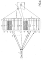
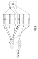
- FIG.4 and FIG.5 respectively show the first and second halves of the data transfer process from a source block B0 to a destination block Bn that the memory controller 6 performs following the data transfer process shown in FIG.3.
- the memory controller 6 first receives a physical address from the address conversion section 4. Then, the memory controller 6 identifies a block corresponding to the physical address as a source block in the flash memory 1. In FIGS. 3 - 5, for example, the head block (the first block) B0 is identified as the source block. The memory controller 6 next reads the page offset "2" of the source block B0 from the redundant area RA of the top page (the first page) P0 of the source block B0. Data items D0, D1, ..., and D31 (numerical values beside the reference symbol D show the logical page numbers of the pages storing the data items) are stored in the data areas DA of the source block B0.
- the logical page numbers of the pages P0-P31 shift from the physical page numbers by the page offset "2" in a cyclic manner, as shown in FIG.3.
- the pages P0, P1, ..., and P31 may include a page in a state of being erased (or a blank page) .
- the difference generally ranges from -31 to 31 inclusive.
- the memory controller 6 identifies the difference as the physical page number of the write target page.
- the physical page number of the write target page is determined as an integer between or equal to 0 and 31.
- the seventh page P6 of the source block B0 is identified as the write target page.
- the memory controller 6 accesses the address-conversion-table storage section 5 and, based on the flags F stored there, selects one of blank blocks in the flash memory 1 as a destination block.
- the (n+1)th block Bn (n ⁇ 1) is selected as the destination block.
- Any of the 32 pages Q0, Q1, ..., and Q31 (numerical values beside the reference symbol Q show physical page numbers) in the destination block Bn is blank.
- the host interface 3 receives data objects DN8-DN12 to be written that is sent from the host H, and writes the data objects into the page buffer 2 page by page.
- the memory controller 6 transfers the data objects DN8-DN12 from the page buffer 2 to the destination block Bn page by page (see the arrow shown in FIG.3.)
- the data objects DN8-DN12 are written page by page, starting from the top page Q0 of the destination block Bn in sequence.
- the memory controller 6 further determines the logical page number "8" of the write target page as the page offset of the destination block Bn, and writes the page offset into the redundant area RA of the top page Q0 of the destination block Bn.
- the memory controller 6 Every time when transferring the data objects DN8-DN12 from the page buffer 2 to the destination block Bn, the memory controller 6 counts the number of times of the transfer.
- the host H notifies the semiconductor memory apparatus 10 of the end of sending of data objects to be written, using a predetermined command.
- the memory controller 6 detects the command through the host interface 3. At the detection of the command, the memory controller 6 determines the number of pages, "5", of the storage region Q0-Q4 of the data objects DN8-DN12, based on the above-described number of times of the transfer. Then, the memory controller 6 further starts the data transfer from the source block B0 to the destination block Bn.
- the host H may provide the semiconductor memory apparatus 10 with prior notification of the page number "5" required for the storage of the data objects DN8-DN12. In that case, when the above-described number of times of the transfer reaches the notified page number "5", the memory controller 6 starts the data transfer from the source block B0 to the destination block Bn.
- the page buffer 2 Before the start of a data transfer from the source block B0 to the destination block Bn (which is hereafter referred to as a block transfer), the page buffer 2 is freed.
- data items D13, ..., D31, D0, and D1 on the transfer start page P11 through the final page (the 32nd page) P31 are transferred to the destination block Bn as follows (see FIG.4): First, the data item D13 on the transfer start page P11 is read into the page buffer 2 (see the arrow R1 shown in FIG.4.) Furthermore, the data item D13 in the page buffer 2 is written onto the sixth page Q5 of the destination block Bn (see the arrow W1 shown in FIG.4.) Next, the data item D14 on the 13th page P12 of the source block B0 is read into the page buffer 2 (see the arrow R2 shown in FIG.4.) Furthermore, the data item D14 in the page buffer 2 is written onto the seventh page Q6 of the destination block Bn (see the arrow W2 shown in FIG.
- the memory controller 6 next transfers data items D2, D3, ..., and D7 of the top page P0 through the page (the sixth page) P5 just before the write target page P6 of the source block B0 to the destination block Bn as follows (see FIG.5): First, the data item D2 on the top page P0 of the source block B0 is read into the page buffer 2 (see the arrow R26 shown in FIG.5.) Furthermore, the data item D2 is written from the page buffer 2 onto the 27th page Q26 of the destination block Bn. Next, the data item D3) on the second page P1 of the source block B0 is similarly transferred via the page buffer 2 to the 28th page Q27 of the destination block Bn. The above-described data transfer via the page buffer 2 is repeated six times.
- the data items D2, D3, ..., and D7 on the top page P0 through the page (the sixth page) P5 just before the write target page P6 of the source block B0 are transferred to the data areas DA of the 27th page Q26 through the final page Q31 of the destination block Bn.
- the physical page number of the transfer start page is equal to the sum of the physical page number of the write target page and the number of pages of the storage region of the data objects to be written.
- the value of the sum minus the total page number is identified as the physical page number of the transfer start page.
- the memory controller 6 transfers the data items on the transfer start page through the page just before the write target page to the destination block Bn in a manner similar to the data transfers shown in FIG. 5 .
- the memory controller 6 disables or collectively erases data items in the source block B0.
- the address conversion section 4 updates the logical/physical address conversion table L, and brings the logical address corresponding to the physical address of the source block B0 into correspondence with the physical address of the destination block Bn.
- the address conversion section 4 further resets the flag F stored in the address-conversion-table storage section 5 to show that the source block B0 is a blank block.
- the memory controller 6 performs the data writing from the page buffer 2 into the destination block Bn, starting from the top page Q0 of the destination block Bn and finishing at the final page Q31 as described above.
- This writing order is the same as that of conventional apparatuses. Accordingly, the same configuration as that of the conventional apparatuses may be used for the data writing from the page buffer into the destination block.
- FIG.6 is the flow chart of the method of writing data by the semiconductor memory apparatus 10.
- a data write command is sent out from the host H.
- the host interface 3 receives the data write command and decodes it into the logical address of a write target page.
- the host interface 3 further sends the logical address to the address conversion section 4.
- the address conversion section 4 receives the logical address from the host interface 3. The address conversion section 4 then consults the logical/physical address conversion table L and converts the logical address into the pair of the physical address of the source block B0 and the logical page number q (0 ⁇ q ⁇ 31) of the write target page. The address conversion section 4 further sends the pair to the memory controller 6.
- the memory controller 6 accesses the address-conversion-table storage section 5 and selects one of blank blocks, Bn in the flash memory 1 as a destination block, based on the flags F.
- the source block B0 is a blank block
- the source block B0 itself may be selected as the destination block Bn. In that case, the following steps S8 and S9 are skipped.
- the memory controller 6 writes the logical page number q received from the address conversion section 4 into the redundant area RA of the top page Q0 of the destination block Bn (see FIG.3.)
- the memory controller 6 reads the page offset p (0 ⁇ p ⁇ 31) of the source block B0 from the redundant area RA of the top page P0 of the source block B0.
- the host interface 3 receives data objects DN(q), DN(q+1), ... to be written from the host H (reference symbols in parentheses beside the reference symbol DN show logical page numbers.)
- the host interface 3 transfers the data objects DN(q), DN(q+1), ... to the page buffer 2 page by page.
- the host interface 3 further notifies the memory controller 6 of the transfer.
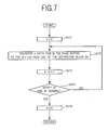
- the memory controller 6 transfers the data objects DN(q), DN(q+1), ... in the page buffer 2 every notification from the host interface 3, starting from the top page Q0 of the destination block Bn in sequence.
- FIG.7 is the flow chart of the transfers.
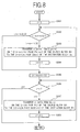
- the memory controller 6 starts a data transfer from the source block B0 to the destination block Bn (a block transfer).
- FIG.8 is the flow chart of the block transfer.
- the data items D(p), ..., and D(q-1) of the first page P0 through the rth page P(r-1) of the source block B0 are transferred to the data areas DA of the (33-r)th page Q(32-r) through the 32nd page (the final page) Q31 of the destination block Bn (see FIG.5.)
- the data items D(q+m), ..., D31, D0, ..., and D(q-1) of the (q+m-p+1)th page P(q+m-p) through the rth page P(r-1) of the source block B0 are transferred to the data areas DA of the (m+1)th page Qm through the 32nd page (the final page) Q31 of the destination block Bn.
- the memory controller 6 collectively erases or disables data items in the source block B0.
- the address conversion section 4 then updates the logical/physical address conversion table L, and brings the logical address corresponding to the physical address of the source block B0 into correspondence with the physical address of the destination block Bn.
- the address conversion section 4 further resets the flag F stored in the address-conversion-table storage section 5 to show that the source block B0 is a blank block.
- the semiconductor memory apparatus 10 uses the page buffer 2 as a saving space of the data items in the original block, thereby including no saving buffer apart from the page buffer 2, in contrast to conventional apparatuses.
- the semiconductor memory apparatus has RAMs smaller in size than those of the conventional apparatuses. Therefore, a small size of the whole apparatus can be maintained.
- the semiconductor memory apparatus realizes miniaturization through the integration of page buffer and saving buffer. Therefore, the present invention has extremely high industrial applicability.
Landscapes
- Engineering & Computer Science (AREA)
- Theoretical Computer Science (AREA)
- Physics & Mathematics (AREA)
- General Engineering & Computer Science (AREA)
- General Physics & Mathematics (AREA)
- Read Only Memory (AREA)
- Techniques For Improving Reliability Of Storages (AREA)
- Memory System (AREA)
Applications Claiming Priority (3)
| Application Number | Priority Date | Filing Date | Title |
|---|---|---|---|
| JP2002251194 | 2002-08-29 | ||
| JP2002251194 | 2002-08-29 | ||
| PCT/JP2003/010718 WO2004021191A1 (ja) | 2002-08-29 | 2003-08-25 | 半導体メモリ装置、及び、フラッシュメモリへのデータ書き込み方法 |
Publications (2)
| Publication Number | Publication Date |
|---|---|
| EP1533702A1 true EP1533702A1 (de) | 2005-05-25 |
| EP1533702A4 EP1533702A4 (de) | 2007-05-23 |
Family
ID=31972668
Family Applications (1)
| Application Number | Title | Priority Date | Filing Date |
|---|---|---|---|
| EP03791270A Withdrawn EP1533702A4 (de) | 2002-08-29 | 2003-08-25 | Halbleiterspeicherbaustein und verfahren zum schreiben von daten in flash-speicher |
Country Status (8)
| Country | Link |
|---|---|
| US (2) | USRE42648E1 (de) |
| EP (1) | EP1533702A4 (de) |
| JP (1) | JP4358111B2 (de) |
| KR (1) | KR100944054B1 (de) |
| CN (2) | CN101114255A (de) |
| CA (1) | CA2461446A1 (de) |
| TW (1) | TWI260535B (de) |
| WO (1) | WO2004021191A1 (de) |
Cited By (2)
| Publication number | Priority date | Publication date | Assignee | Title |
|---|---|---|---|---|
| CN102722456A (zh) * | 2012-05-30 | 2012-10-10 | 深圳市江波龙电子有限公司 | 闪存存储设备的数据写入方法和闪存存储设备 |
| CN103019616A (zh) * | 2012-11-23 | 2013-04-03 | 记忆科技(深圳)有限公司 | 一种固态硬盘及闪存芯片的充放电控制方法 |
Families Citing this family (352)
| Publication number | Priority date | Publication date | Assignee | Title |
|---|---|---|---|---|
| US7321959B2 (en) * | 2002-10-02 | 2008-01-22 | Matsushita Electric Industrial Co., Ltd. | Control method of a non-volatile memory apparatus |
| JP4253272B2 (ja) | 2004-05-27 | 2009-04-08 | 株式会社東芝 | メモリカード、半導体装置、及び半導体メモリの制御方法 |
| US7383414B2 (en) * | 2004-05-28 | 2008-06-03 | Oracle International Corporation | Method and apparatus for memory-mapped input/output |
| JP3969494B2 (ja) * | 2004-08-31 | 2007-09-05 | 三菱電機株式会社 | 車載電子制御装置 |
| JP2006085380A (ja) * | 2004-09-15 | 2006-03-30 | Toshiba Corp | ファイルストレージデバイス、プログラム、及び不揮発性半導体メモリの書込方法 |
| US7409623B2 (en) * | 2004-11-04 | 2008-08-05 | Sigmatel, Inc. | System and method of reading non-volatile computer memory |
| KR100706242B1 (ko) * | 2005-02-07 | 2007-04-11 | 삼성전자주식회사 | 메모리 시스템 및 그것의 런 단위 어드레스 매핑 테이블 구성 방법 |
| JP5130646B2 (ja) | 2005-06-06 | 2013-01-30 | ソニー株式会社 | 記憶装置 |
| JP4688584B2 (ja) * | 2005-06-21 | 2011-05-25 | 株式会社日立製作所 | ストレージ装置 |
| KR101197556B1 (ko) * | 2006-01-09 | 2012-11-09 | 삼성전자주식회사 | 불 휘발성 메모리의 프로그램 동작을 검증하는 장치 및방법, 그리고 그 장치를 포함한 메모리 카드 |
| JP2007199905A (ja) * | 2006-01-25 | 2007-08-09 | Toshiba Corp | 半導体記憶装置の制御方法 |
| CN101288056A (zh) | 2006-03-13 | 2008-10-15 | 松下电器产业株式会社 | 闪速存储器用的存储控制器 |
| US7996598B2 (en) * | 2006-03-14 | 2011-08-09 | Stmicroelectronics Pvt. Ltd. | Memory management module |
| JP2008009527A (ja) * | 2006-06-27 | 2008-01-17 | Toshiba Corp | メモリシステム |
| KR100816148B1 (ko) * | 2006-09-29 | 2008-03-21 | 주식회사 하이닉스반도체 | 플래시 메모리 소자 및 이의 독출 방법 |
| CN101105774B (zh) * | 2006-10-26 | 2010-08-11 | 福昭科技(深圳)有限公司 | 闪存记忆体在进行数据存取时的逻辑与物理地址转换方法 |
| TWI326028B (en) | 2006-11-20 | 2010-06-11 | Silicon Motion Inc | Method for flash memory data management |
| CN101196851B (zh) * | 2006-12-05 | 2011-09-07 | 慧荣科技股份有限公司 | 闪存的数据管理方法 |
| DE602008003150D1 (de) * | 2007-05-02 | 2010-12-09 | St Microelectronics Sa | Nicht flüchtiger Speicher mit partieller Löschung |
| US7962683B2 (en) * | 2007-08-15 | 2011-06-14 | Silicon Motion, Inc. | Flash memory, and method for operating a flash memory |
| US20090144458A1 (en) * | 2007-12-03 | 2009-06-04 | Broadcom Corporation | Dongle device and host device with millimeter wave host inerface and method for use therewith |
| CN101256564B (zh) * | 2007-12-25 | 2010-06-02 | 深圳市同洲电子股份有限公司 | 一种循环文件的操作方法 |
| US8566505B2 (en) * | 2008-04-15 | 2013-10-22 | SMART Storage Systems, Inc. | Flash management using sequential techniques |
| WO2009129340A2 (en) * | 2008-04-15 | 2009-10-22 | Adtron, Inc. | Flash memory management |
| US8180954B2 (en) * | 2008-04-15 | 2012-05-15 | SMART Storage Systems, Inc. | Flash management using logical page size |
| US8185778B2 (en) * | 2008-04-15 | 2012-05-22 | SMART Storage Systems, Inc. | Flash management using separate metadata storage |
| US20090259806A1 (en) * | 2008-04-15 | 2009-10-15 | Adtron, Inc. | Flash management using bad page tracking and high defect flash memory |
| US8028123B2 (en) * | 2008-04-15 | 2011-09-27 | SMART Modular Technologies (AZ) , Inc. | Circular wear leveling |
| US8555086B2 (en) * | 2008-06-30 | 2013-10-08 | Intel Corporation | Encrypting data on a non-volatile memory |
| CN101673245B (zh) * | 2008-09-09 | 2016-02-03 | 株式会社东芝 | 包括存储器管理装置的信息处理装置和存储器管理方法 |
| CN101676885B (zh) * | 2008-09-17 | 2013-08-21 | 群联电子股份有限公司 | 数据管理方法及其存储装置与其控制器 |
| US8566562B2 (en) * | 2008-10-03 | 2013-10-22 | Skymedi Corporation | Method for sequentially writing data with an offset to a non-volatile memory |
| US8296503B2 (en) * | 2009-05-26 | 2012-10-23 | Mediatek Inc. | Data updating and recovering methods for a non-volatile memory array |
| TWI426384B (zh) * | 2009-09-10 | 2014-02-11 | Robustflash Technologies Ltd | 資料寫入方法與系統 |
| CN101673243B (zh) * | 2009-09-29 | 2011-09-07 | 威盛电子股份有限公司 | 数据储存装置与方法 |
| TWI437569B (zh) * | 2009-10-16 | 2014-05-11 | Silicon Motion Inc | 用來管理一快閃記憶體的複數個區塊之方法以及相關之記憶裝置及其控制器 |
| TWI416525B (zh) * | 2009-12-15 | 2013-11-21 | Asolid Technology Co Ltd | 非揮發性記憶體裝置及其損耗平均方法 |
| US8381018B2 (en) | 2010-05-21 | 2013-02-19 | Mediatek Inc. | Method for data recovery for flash devices |
| US12613638B2 (en) | 2010-09-15 | 2026-04-28 | Everpure, Inc. | Efficient execution of I/O operations in a storage environment |
| US11614893B2 (en) | 2010-09-15 | 2023-03-28 | Pure Storage, Inc. | Optimizing storage device access based on latency |
| US9244769B2 (en) | 2010-09-28 | 2016-01-26 | Pure Storage, Inc. | Offset protection data in a RAID array |
| US8775868B2 (en) | 2010-09-28 | 2014-07-08 | Pure Storage, Inc. | Adaptive RAID for an SSD environment |
| US8909851B2 (en) | 2011-02-08 | 2014-12-09 | SMART Storage Systems, Inc. | Storage control system with change logging mechanism and method of operation thereof |
| US8935466B2 (en) | 2011-03-28 | 2015-01-13 | SMART Storage Systems, Inc. | Data storage system with non-volatile memory and method of operation thereof |
| US11636031B2 (en) | 2011-08-11 | 2023-04-25 | Pure Storage, Inc. | Optimized inline deduplication |
| US9098399B2 (en) | 2011-08-31 | 2015-08-04 | SMART Storage Systems, Inc. | Electronic system with storage management mechanism and method of operation thereof |
| US9021231B2 (en) | 2011-09-02 | 2015-04-28 | SMART Storage Systems, Inc. | Storage control system with write amplification control mechanism and method of operation thereof |
| US9021319B2 (en) | 2011-09-02 | 2015-04-28 | SMART Storage Systems, Inc. | Non-volatile memory management system with load leveling and method of operation thereof |
| US9063844B2 (en) | 2011-09-02 | 2015-06-23 | SMART Storage Systems, Inc. | Non-volatile memory management system with time measure mechanism and method of operation thereof |
| US8797799B2 (en) * | 2012-01-05 | 2014-08-05 | Conversant Intellectual Property Management Inc. | Device selection schemes in multi chip package NAND flash memory system |
| US9239781B2 (en) | 2012-02-07 | 2016-01-19 | SMART Storage Systems, Inc. | Storage control system with erase block mechanism and method of operation thereof |
| US9298252B2 (en) | 2012-04-17 | 2016-03-29 | SMART Storage Systems, Inc. | Storage control system with power down mechanism and method of operation thereof |
| TWI486766B (zh) * | 2012-05-11 | 2015-06-01 | Phison Electronics Corp | 資料處理方法、記憶體控制器與記憶體儲存裝置 |
| US8949689B2 (en) | 2012-06-11 | 2015-02-03 | SMART Storage Systems, Inc. | Storage control system with data management mechanism and method of operation thereof |
| US11032259B1 (en) | 2012-09-26 | 2021-06-08 | Pure Storage, Inc. | Data protection in a storage system |
| US9671962B2 (en) | 2012-11-30 | 2017-06-06 | Sandisk Technologies Llc | Storage control system with data management mechanism of parity and method of operation thereof |
| US9646039B2 (en) | 2013-01-10 | 2017-05-09 | Pure Storage, Inc. | Snapshots in a storage system |
| US11733908B2 (en) | 2013-01-10 | 2023-08-22 | Pure Storage, Inc. | Delaying deletion of a dataset |
| US9123445B2 (en) | 2013-01-22 | 2015-09-01 | SMART Storage Systems, Inc. | Storage control system with data management mechanism and method of operation thereof |
| US9214965B2 (en) | 2013-02-20 | 2015-12-15 | Sandisk Enterprise Ip Llc | Method and system for improving data integrity in non-volatile storage |
| US9329928B2 (en) | 2013-02-20 | 2016-05-03 | Sandisk Enterprise IP LLC. | Bandwidth optimization in a non-volatile memory system |
| US9183137B2 (en) | 2013-02-27 | 2015-11-10 | SMART Storage Systems, Inc. | Storage control system with data management mechanism and method of operation thereof |
| US9470720B2 (en) | 2013-03-08 | 2016-10-18 | Sandisk Technologies Llc | Test system with localized heating and method of manufacture thereof |
| US9043780B2 (en) | 2013-03-27 | 2015-05-26 | SMART Storage Systems, Inc. | Electronic system with system modification control mechanism and method of operation thereof |
| US10049037B2 (en) | 2013-04-05 | 2018-08-14 | Sandisk Enterprise Ip Llc | Data management in a storage system |
| US9170941B2 (en) | 2013-04-05 | 2015-10-27 | Sandisk Enterprises IP LLC | Data hardening in a storage system |
| US9543025B2 (en) | 2013-04-11 | 2017-01-10 | Sandisk Technologies Llc | Storage control system with power-off time estimation mechanism and method of operation thereof |
| US10546648B2 (en) | 2013-04-12 | 2020-01-28 | Sandisk Technologies Llc | Storage control system with data management mechanism and method of operation thereof |
| US9313874B2 (en) | 2013-06-19 | 2016-04-12 | SMART Storage Systems, Inc. | Electronic system with heat extraction and method of manufacture thereof |
| US9898056B2 (en) | 2013-06-19 | 2018-02-20 | Sandisk Technologies Llc | Electronic assembly with thermal channel and method of manufacture thereof |
| US9367353B1 (en) | 2013-06-25 | 2016-06-14 | Sandisk Technologies Inc. | Storage control system with power throttling mechanism and method of operation thereof |
| US9244519B1 (en) | 2013-06-25 | 2016-01-26 | Smart Storage Systems. Inc. | Storage system with data transfer rate adjustment for power throttling |
| US9146850B2 (en) | 2013-08-01 | 2015-09-29 | SMART Storage Systems, Inc. | Data storage system with dynamic read threshold mechanism and method of operation thereof |
| US9431113B2 (en) | 2013-08-07 | 2016-08-30 | Sandisk Technologies Llc | Data storage system with dynamic erase block grouping mechanism and method of operation thereof |
| US9361222B2 (en) | 2013-08-07 | 2016-06-07 | SMART Storage Systems, Inc. | Electronic system with storage drive life estimation mechanism and method of operation thereof |
| US9448946B2 (en) | 2013-08-07 | 2016-09-20 | Sandisk Technologies Llc | Data storage system with stale data mechanism and method of operation thereof |
| US12574220B2 (en) | 2013-11-06 | 2026-03-10 | Pure Storage, Inc. | Sharing encryption information amongst storage devices in a storage system |
| US11630585B1 (en) | 2016-08-25 | 2023-04-18 | Pure Storage, Inc. | Processing evacuation events in a storage array that includes a plurality of storage devices |
| US9152555B2 (en) | 2013-11-15 | 2015-10-06 | Sandisk Enterprise IP LLC. | Data management with modular erase in a data storage system |
| CN103778964B (zh) * | 2013-12-30 | 2016-08-17 | 上海晨思电子科技有限公司 | 一种NAND Flash烧写数据的处理、使用方法及装置、系统 |
| JP2015138272A (ja) * | 2014-01-20 | 2015-07-30 | ソニー株式会社 | 情報処理装置、情報処理方法、および情報処理プログラム |
| US10656864B2 (en) | 2014-03-20 | 2020-05-19 | Pure Storage, Inc. | Data replication within a flash storage array |
| US9779268B1 (en) | 2014-06-03 | 2017-10-03 | Pure Storage, Inc. | Utilizing a non-repeating identifier to encrypt data |
| US8976609B1 (en) | 2014-06-16 | 2015-03-10 | Sandisk Enterprise Ip Llc | Low-test memory stack for non-volatile storage |
| US9653184B2 (en) | 2014-06-16 | 2017-05-16 | Sandisk Technologies Llc | Non-volatile memory module with physical-to-physical address remapping |
| US9613715B2 (en) | 2014-06-16 | 2017-04-04 | Sandisk Technologies Llc | Low-test memory stack for non-volatile storage |
| CN104166627B (zh) * | 2014-09-02 | 2017-12-08 | 科大智能电气技术有限公司 | 一种基于单片机的nand‑flash写操作方法 |
| US12175076B2 (en) | 2014-09-08 | 2024-12-24 | Pure Storage, Inc. | Projecting capacity utilization for snapshots |
| US10430079B2 (en) | 2014-09-08 | 2019-10-01 | Pure Storage, Inc. | Adjusting storage capacity in a computing system |
| US10164841B2 (en) | 2014-10-02 | 2018-12-25 | Pure Storage, Inc. | Cloud assist for storage systems |
| US9489132B2 (en) | 2014-10-07 | 2016-11-08 | Pure Storage, Inc. | Utilizing unmapped and unknown states in a replicated storage system |
| US10545987B2 (en) | 2014-12-19 | 2020-01-28 | Pure Storage, Inc. | Replication to the cloud |
| US11102298B1 (en) | 2015-05-26 | 2021-08-24 | Pure Storage, Inc. | Locally providing cloud storage services for fleet management |
| US9716755B2 (en) | 2015-05-26 | 2017-07-25 | Pure Storage, Inc. | Providing cloud storage array services by a local storage array in a data center |
| US9594678B1 (en) | 2015-05-27 | 2017-03-14 | Pure Storage, Inc. | Preventing duplicate entries of identical data in a storage device |
| US10021170B2 (en) | 2015-05-29 | 2018-07-10 | Pure Storage, Inc. | Managing a storage array using client-side services |
| US11503031B1 (en) | 2015-05-29 | 2022-11-15 | Pure Storage, Inc. | Storage array access control from cloud-based user authorization and authentication |
| US9444822B1 (en) | 2015-05-29 | 2016-09-13 | Pure Storage, Inc. | Storage array access control from cloud-based user authorization and authentication |
| US9300660B1 (en) | 2015-05-29 | 2016-03-29 | Pure Storage, Inc. | Providing authorization and authentication in a cloud for a user of a storage array |
| US9588691B2 (en) | 2015-06-10 | 2017-03-07 | Pure Storage, Inc. | Dynamically managing control information in a storage device |
| US9594512B1 (en) | 2015-06-19 | 2017-03-14 | Pure Storage, Inc. | Attributing consumed storage capacity among entities storing data in a storage array |
| US12561068B2 (en) | 2015-06-19 | 2026-02-24 | Pure Storage, Inc. | Calculating storage consumption in a storage-as-a-service model |
| US9547441B1 (en) | 2015-06-23 | 2017-01-17 | Pure Storage, Inc. | Exposing a geometry of a storage device |
| US10310740B2 (en) * | 2015-06-23 | 2019-06-04 | Pure Storage, Inc. | Aligning memory access operations to a geometry of a storage device |
| US10296236B2 (en) | 2015-07-01 | 2019-05-21 | Pure Storage, Inc. | Offloading device management responsibilities from a storage device in an array of storage devices |
| US9892071B2 (en) | 2015-08-03 | 2018-02-13 | Pure Storage, Inc. | Emulating a remote direct memory access (‘RDMA’) link between controllers in a storage array |
| US9851762B1 (en) | 2015-08-06 | 2017-12-26 | Pure Storage, Inc. | Compliant printed circuit board (‘PCB’) within an enclosure |
| US11625181B1 (en) | 2015-08-24 | 2023-04-11 | Pure Storage, Inc. | Data tiering using snapshots |
| US10572460B2 (en) | 2016-02-11 | 2020-02-25 | Pure Storage, Inc. | Compressing data in dependence upon characteristics of a storage system |
| US11294588B1 (en) | 2015-08-24 | 2022-04-05 | Pure Storage, Inc. | Placing data within a storage device |
| US10198194B2 (en) | 2015-08-24 | 2019-02-05 | Pure Storage, Inc. | Placing data within a storage device of a flash array |
| US10514978B1 (en) | 2015-10-23 | 2019-12-24 | Pure Storage, Inc. | Automatic deployment of corrective measures for storage arrays |
| US11360844B1 (en) | 2015-10-23 | 2022-06-14 | Pure Storage, Inc. | Recovery of a container storage provider |
| US9384082B1 (en) | 2015-10-23 | 2016-07-05 | Pure Storage, Inc. | Proactively providing corrective measures for storage arrays |
| US10284232B2 (en) | 2015-10-28 | 2019-05-07 | Pure Storage, Inc. | Dynamic error processing in a storage device |
| US9740414B2 (en) | 2015-10-29 | 2017-08-22 | Pure Storage, Inc. | Optimizing copy operations |
| US10374868B2 (en) | 2015-10-29 | 2019-08-06 | Pure Storage, Inc. | Distributed command processing in a flash storage system |
| US10353777B2 (en) | 2015-10-30 | 2019-07-16 | Pure Storage, Inc. | Ensuring crash-safe forward progress of a system configuration update |
| US12182014B2 (en) | 2015-11-02 | 2024-12-31 | Pure Storage, Inc. | Cost effective storage management |
| US11762764B1 (en) | 2015-12-02 | 2023-09-19 | Pure Storage, Inc. | Writing data in a storage system that includes a first type of storage device and a second type of storage device |
| US9760479B2 (en) | 2015-12-02 | 2017-09-12 | Pure Storage, Inc. | Writing data in a storage system that includes a first type of storage device and a second type of storage device |
| US10326836B2 (en) | 2015-12-08 | 2019-06-18 | Pure Storage, Inc. | Partially replicating a snapshot between storage systems |
| US11616834B2 (en) | 2015-12-08 | 2023-03-28 | Pure Storage, Inc. | Efficient replication of a dataset to the cloud |
| US10162835B2 (en) | 2015-12-15 | 2018-12-25 | Pure Storage, Inc. | Proactive management of a plurality of storage arrays in a multi-array system |
| US11347697B1 (en) | 2015-12-15 | 2022-05-31 | Pure Storage, Inc. | Proactively optimizing a storage system |
| US10346043B2 (en) | 2015-12-28 | 2019-07-09 | Pure Storage, Inc. | Adaptive computing for data compression |
| US9886314B2 (en) | 2016-01-28 | 2018-02-06 | Pure Storage, Inc. | Placing workloads in a multi-array system |
| US12253990B2 (en) | 2016-02-11 | 2025-03-18 | Pure Storage, Inc. | Tier-specific data compression |
| US9760297B2 (en) | 2016-02-12 | 2017-09-12 | Pure Storage, Inc. | Managing input/output (‘I/O’) queues in a data storage system |
| US9959043B2 (en) | 2016-03-16 | 2018-05-01 | Pure Storage, Inc. | Performing a non-disruptive upgrade of data in a storage system |
| US11995315B2 (en) | 2016-03-16 | 2024-05-28 | Pure Storage, Inc. | Converting data formats in a storage system |
| US11112990B1 (en) | 2016-04-27 | 2021-09-07 | Pure Storage, Inc. | Managing storage device evacuation |
| US11809727B1 (en) | 2016-04-27 | 2023-11-07 | Pure Storage, Inc. | Predicting failures in a storage system that includes a plurality of storage devices |
| US9841921B2 (en) | 2016-04-27 | 2017-12-12 | Pure Storage, Inc. | Migrating data in a storage array that includes a plurality of storage devices |
| US9811264B1 (en) | 2016-04-28 | 2017-11-07 | Pure Storage, Inc. | Deploying client-specific applications in a storage system utilizing redundant system resources |
| US10303390B1 (en) | 2016-05-02 | 2019-05-28 | Pure Storage, Inc. | Resolving fingerprint collisions in flash storage system |
| US11231858B2 (en) | 2016-05-19 | 2022-01-25 | Pure Storage, Inc. | Dynamically configuring a storage system to facilitate independent scaling of resources |
| US9507532B1 (en) | 2016-05-20 | 2016-11-29 | Pure Storage, Inc. | Migrating data in a storage array that includes a plurality of storage devices and a plurality of write buffer devices |
| US10691567B2 (en) | 2016-06-03 | 2020-06-23 | Pure Storage, Inc. | Dynamically forming a failure domain in a storage system that includes a plurality of blades |
| US10452310B1 (en) | 2016-07-13 | 2019-10-22 | Pure Storage, Inc. | Validating cabling for storage component admission to a storage array |
| US11706895B2 (en) | 2016-07-19 | 2023-07-18 | Pure Storage, Inc. | Independent scaling of compute resources and storage resources in a storage system |
| US10459652B2 (en) | 2016-07-27 | 2019-10-29 | Pure Storage, Inc. | Evacuating blades in a storage array that includes a plurality of blades |
| US10474363B1 (en) | 2016-07-29 | 2019-11-12 | Pure Storage, Inc. | Space reporting in a storage system |
| US11886922B2 (en) | 2016-09-07 | 2024-01-30 | Pure Storage, Inc. | Scheduling input/output operations for a storage system |
| US11531577B1 (en) | 2016-09-07 | 2022-12-20 | Pure Storage, Inc. | Temporarily limiting access to a storage device |
| US10331588B2 (en) | 2016-09-07 | 2019-06-25 | Pure Storage, Inc. | Ensuring the appropriate utilization of system resources using weighted workload based, time-independent scheduling |
| US10235229B1 (en) | 2016-09-07 | 2019-03-19 | Pure Storage, Inc. | Rehabilitating storage devices in a storage array that includes a plurality of storage devices |
| US10146585B2 (en) | 2016-09-07 | 2018-12-04 | Pure Storage, Inc. | Ensuring the fair utilization of system resources using workload based, time-independent scheduling |
| US12461803B2 (en) | 2016-09-07 | 2025-11-04 | Pure Storage, Inc. | Determining remaining hardware life in a storage device |
| US10908966B1 (en) | 2016-09-07 | 2021-02-02 | Pure Storage, Inc. | Adapting target service times in a storage system |
| US10671439B1 (en) | 2016-09-07 | 2020-06-02 | Pure Storage, Inc. | Workload planning with quality-of-service (‘QOS’) integration |
| US11481261B1 (en) | 2016-09-07 | 2022-10-25 | Pure Storage, Inc. | Preventing extended latency in a storage system |
| US11960348B2 (en) | 2016-09-07 | 2024-04-16 | Pure Storage, Inc. | Cloud-based monitoring of hardware components in a fleet of storage systems |
| US10007459B2 (en) | 2016-10-20 | 2018-06-26 | Pure Storage, Inc. | Performance tuning in a storage system that includes one or more storage devices |
| US11379132B1 (en) | 2016-10-20 | 2022-07-05 | Pure Storage, Inc. | Correlating medical sensor data |
| US12405735B2 (en) | 2016-10-20 | 2025-09-02 | Pure Storage, Inc. | Configuring storage systems based on storage utilization patterns |
| US10162566B2 (en) | 2016-11-22 | 2018-12-25 | Pure Storage, Inc. | Accumulating application-level statistics in a storage system |
| US11620075B2 (en) | 2016-11-22 | 2023-04-04 | Pure Storage, Inc. | Providing application aware storage |
| US10198205B1 (en) | 2016-12-19 | 2019-02-05 | Pure Storage, Inc. | Dynamically adjusting a number of storage devices utilized to simultaneously service write operations |
| US11461273B1 (en) | 2016-12-20 | 2022-10-04 | Pure Storage, Inc. | Modifying storage distribution in a storage system that includes one or more storage devices |
| US10489307B2 (en) | 2017-01-05 | 2019-11-26 | Pure Storage, Inc. | Periodically re-encrypting user data stored on a storage device |
| US12282436B2 (en) | 2017-01-05 | 2025-04-22 | Pure Storage, Inc. | Instant rekey in a storage system |
| US11307998B2 (en) | 2017-01-09 | 2022-04-19 | Pure Storage, Inc. | Storage efficiency of encrypted host system data |
| US10503700B1 (en) | 2017-01-19 | 2019-12-10 | Pure Storage, Inc. | On-demand content filtering of snapshots within a storage system |
| US11340800B1 (en) | 2017-01-19 | 2022-05-24 | Pure Storage, Inc. | Content masking in a storage system |
| US11163624B2 (en) | 2017-01-27 | 2021-11-02 | Pure Storage, Inc. | Dynamically adjusting an amount of log data generated for a storage system |
| US11941279B2 (en) | 2017-03-10 | 2024-03-26 | Pure Storage, Inc. | Data path virtualization |
| US12056383B2 (en) | 2017-03-10 | 2024-08-06 | Pure Storage, Inc. | Edge management service |
| US11169727B1 (en) | 2017-03-10 | 2021-11-09 | Pure Storage, Inc. | Synchronous replication between storage systems with virtualized storage |
| US10521344B1 (en) | 2017-03-10 | 2019-12-31 | Pure Storage, Inc. | Servicing input/output (‘I/O’) operations directed to a dataset that is synchronized across a plurality of storage systems |
| US11803453B1 (en) | 2017-03-10 | 2023-10-31 | Pure Storage, Inc. | Using host connectivity states to avoid queuing I/O requests |
| US10503427B2 (en) | 2017-03-10 | 2019-12-10 | Pure Storage, Inc. | Synchronously replicating datasets and other managed objects to cloud-based storage systems |
| US11442825B2 (en) | 2017-03-10 | 2022-09-13 | Pure Storage, Inc. | Establishing a synchronous replication relationship between two or more storage systems |
| US11089105B1 (en) | 2017-12-14 | 2021-08-10 | Pure Storage, Inc. | Synchronously replicating datasets in cloud-based storage systems |
| US12511068B2 (en) | 2017-03-10 | 2025-12-30 | Pure Storage, Inc. | Fan out data replication in a storage system |
| US11675520B2 (en) | 2017-03-10 | 2023-06-13 | Pure Storage, Inc. | Application replication among storage systems synchronously replicating a dataset |
| US10454810B1 (en) | 2017-03-10 | 2019-10-22 | Pure Storage, Inc. | Managing host definitions across a plurality of storage systems |
| US12348583B2 (en) | 2017-03-10 | 2025-07-01 | Pure Storage, Inc. | Replication utilizing cloud-based storage systems |
| US12411739B2 (en) | 2017-03-10 | 2025-09-09 | Pure Storage, Inc. | Initiating recovery actions when a dataset ceases to be synchronously replicated across a set of storage systems |
| US9910618B1 (en) | 2017-04-10 | 2018-03-06 | Pure Storage, Inc. | Migrating applications executing on a storage system |
| US10459664B1 (en) | 2017-04-10 | 2019-10-29 | Pure Storage, Inc. | Virtualized copy-by-reference |
| US11868629B1 (en) | 2017-05-05 | 2024-01-09 | Pure Storage, Inc. | Storage system sizing service |
| US10417092B2 (en) | 2017-09-07 | 2019-09-17 | Pure Storage, Inc. | Incremental RAID stripe update parity calculation |
| US12086650B2 (en) | 2017-06-12 | 2024-09-10 | Pure Storage, Inc. | Workload placement based on carbon emissions |
| US11210133B1 (en) | 2017-06-12 | 2021-12-28 | Pure Storage, Inc. | Workload mobility between disparate execution environments |
| US10853148B1 (en) | 2017-06-12 | 2020-12-01 | Pure Storage, Inc. | Migrating workloads between a plurality of execution environments |
| US11016824B1 (en) | 2017-06-12 | 2021-05-25 | Pure Storage, Inc. | Event identification with out-of-order reporting in a cloud-based environment |
| US12229405B2 (en) | 2017-06-12 | 2025-02-18 | Pure Storage, Inc. | Application-aware management of a storage system |
| CN116431072A (zh) | 2017-06-12 | 2023-07-14 | 净睿存储股份有限公司 | 集成到大容量存储设备的可访问快速耐久存储 |
| US11609718B1 (en) | 2017-06-12 | 2023-03-21 | Pure Storage, Inc. | Identifying valid data after a storage system recovery |
| US12669965B2 (en) | 2017-06-12 | 2026-06-30 | Everpure, Inc. | Utilizing generative artificial intelligence to improve storage system management |
| US11442669B1 (en) | 2018-03-15 | 2022-09-13 | Pure Storage, Inc. | Orchestrating a virtual storage system |
| US10976962B2 (en) | 2018-03-15 | 2021-04-13 | Pure Storage, Inc. | Servicing I/O operations in a cloud-based storage system |
| US12086651B2 (en) | 2017-06-12 | 2024-09-10 | Pure Storage, Inc. | Migrating workloads using active disaster recovery |
| US10613791B2 (en) | 2017-06-12 | 2020-04-07 | Pure Storage, Inc. | Portable snapshot replication between storage systems |
| US11592991B2 (en) | 2017-09-07 | 2023-02-28 | Pure Storage, Inc. | Converting raid data between persistent storage types |
| US10884636B1 (en) | 2017-06-12 | 2021-01-05 | Pure Storage, Inc. | Presenting workload performance in a storage system |
| US12061822B1 (en) | 2017-06-12 | 2024-08-13 | Pure Storage, Inc. | Utilizing volume-level policies in a storage system |
| US10789020B2 (en) | 2017-06-12 | 2020-09-29 | Pure Storage, Inc. | Recovering data within a unified storage element |
| US11422731B1 (en) | 2017-06-12 | 2022-08-23 | Pure Storage, Inc. | Metadata-based replication of a dataset |
| US11989429B1 (en) | 2017-06-12 | 2024-05-21 | Pure Storage, Inc. | Recommending changes to a storage system |
| US10552090B2 (en) | 2017-09-07 | 2020-02-04 | Pure Storage, Inc. | Solid state drives with multiple types of addressable memory |
| US11340939B1 (en) | 2017-06-12 | 2022-05-24 | Pure Storage, Inc. | Application-aware analytics for storage systems |
| US11561714B1 (en) | 2017-07-05 | 2023-01-24 | Pure Storage, Inc. | Storage efficiency driven migration |
| US11477280B1 (en) | 2017-07-26 | 2022-10-18 | Pure Storage, Inc. | Integrating cloud storage services |
| US10831935B2 (en) | 2017-08-31 | 2020-11-10 | Pure Storage, Inc. | Encryption management with host-side data reduction |
| US11861423B1 (en) | 2017-10-19 | 2024-01-02 | Pure Storage, Inc. | Accelerating artificial intelligence (‘AI’) workflows |
| US10452444B1 (en) | 2017-10-19 | 2019-10-22 | Pure Storage, Inc. | Storage system with compute resources and shared storage resources |
| US11455168B1 (en) | 2017-10-19 | 2022-09-27 | Pure Storage, Inc. | Batch building for deep learning training workloads |
| US10360214B2 (en) | 2017-10-19 | 2019-07-23 | Pure Storage, Inc. | Ensuring reproducibility in an artificial intelligence infrastructure |
| US10671434B1 (en) | 2017-10-19 | 2020-06-02 | Pure Storage, Inc. | Storage based artificial intelligence infrastructure |
| US12067466B2 (en) | 2017-10-19 | 2024-08-20 | Pure Storage, Inc. | Artificial intelligence and machine learning hyperscale infrastructure |
| US11494692B1 (en) | 2018-03-26 | 2022-11-08 | Pure Storage, Inc. | Hyperscale artificial intelligence and machine learning infrastructure |
| US10671494B1 (en) | 2017-11-01 | 2020-06-02 | Pure Storage, Inc. | Consistent selection of replicated datasets during storage system recovery |
| US10509581B1 (en) | 2017-11-01 | 2019-12-17 | Pure Storage, Inc. | Maintaining write consistency in a multi-threaded storage system |
| US10484174B1 (en) | 2017-11-01 | 2019-11-19 | Pure Storage, Inc. | Protecting an encryption key for data stored in a storage system that includes a plurality of storage devices |
| US10467107B1 (en) | 2017-11-01 | 2019-11-05 | Pure Storage, Inc. | Maintaining metadata resiliency among storage device failures |
| US10817392B1 (en) | 2017-11-01 | 2020-10-27 | Pure Storage, Inc. | Ensuring resiliency to storage device failures in a storage system that includes a plurality of storage devices |
| US10929226B1 (en) | 2017-11-21 | 2021-02-23 | Pure Storage, Inc. | Providing for increased flexibility for large scale parity |
| US10990282B1 (en) | 2017-11-28 | 2021-04-27 | Pure Storage, Inc. | Hybrid data tiering with cloud storage |
| US12393332B2 (en) | 2017-11-28 | 2025-08-19 | Pure Storage, Inc. | Providing storage services and managing a pool of storage resources |
| US10936238B2 (en) | 2017-11-28 | 2021-03-02 | Pure Storage, Inc. | Hybrid data tiering |
| US10795598B1 (en) | 2017-12-07 | 2020-10-06 | Pure Storage, Inc. | Volume migration for storage systems synchronously replicating a dataset |
| US11036677B1 (en) | 2017-12-14 | 2021-06-15 | Pure Storage, Inc. | Replicated data integrity |
| US10929031B2 (en) | 2017-12-21 | 2021-02-23 | Pure Storage, Inc. | Maximizing data reduction in a partially encrypted volume |
| US10992533B1 (en) | 2018-01-30 | 2021-04-27 | Pure Storage, Inc. | Policy based path management |
| US10521151B1 (en) | 2018-03-05 | 2019-12-31 | Pure Storage, Inc. | Determining effective space utilization in a storage system |
| US11861170B2 (en) | 2018-03-05 | 2024-01-02 | Pure Storage, Inc. | Sizing resources for a replication target |
| US11150834B1 (en) | 2018-03-05 | 2021-10-19 | Pure Storage, Inc. | Determining storage consumption in a storage system |
| US11972134B2 (en) | 2018-03-05 | 2024-04-30 | Pure Storage, Inc. | Resource utilization using normalized input/output (‘I/O’) operations |
| US10942650B1 (en) | 2018-03-05 | 2021-03-09 | Pure Storage, Inc. | Reporting capacity utilization in a storage system |
| US10296258B1 (en) | 2018-03-09 | 2019-05-21 | Pure Storage, Inc. | Offloading data storage to a decentralized storage network |
| US11288138B1 (en) | 2018-03-15 | 2022-03-29 | Pure Storage, Inc. | Recovery from a system fault in a cloud-based storage system |
| US12066900B2 (en) | 2018-03-15 | 2024-08-20 | Pure Storage, Inc. | Managing disaster recovery to cloud computing environment |
| US10917471B1 (en) | 2018-03-15 | 2021-02-09 | Pure Storage, Inc. | Active membership in a cloud-based storage system |
| US11210009B1 (en) | 2018-03-15 | 2021-12-28 | Pure Storage, Inc. | Staging data in a cloud-based storage system |
| US10924548B1 (en) | 2018-03-15 | 2021-02-16 | Pure Storage, Inc. | Symmetric storage using a cloud-based storage system |
| US11048590B1 (en) | 2018-03-15 | 2021-06-29 | Pure Storage, Inc. | Data consistency during recovery in a cloud-based storage system |
| US11171950B1 (en) | 2018-03-21 | 2021-11-09 | Pure Storage, Inc. | Secure cloud-based storage system management |
| US11095706B1 (en) | 2018-03-21 | 2021-08-17 | Pure Storage, Inc. | Secure cloud-based storage system management |
| US10838833B1 (en) | 2018-03-26 | 2020-11-17 | Pure Storage, Inc. | Providing for high availability in a data analytics pipeline without replicas |
| US11392553B1 (en) | 2018-04-24 | 2022-07-19 | Pure Storage, Inc. | Remote data management |
| US11436344B1 (en) | 2018-04-24 | 2022-09-06 | Pure Storage, Inc. | Secure encryption in deduplication cluster |
| US12181981B1 (en) | 2018-05-21 | 2024-12-31 | Pure Storage, Inc. | Asynchronously protecting a synchronously replicated dataset |
| US11675503B1 (en) | 2018-05-21 | 2023-06-13 | Pure Storage, Inc. | Role-based data access |
| US11954220B2 (en) | 2018-05-21 | 2024-04-09 | Pure Storage, Inc. | Data protection for container storage |
| US10992598B2 (en) | 2018-05-21 | 2021-04-27 | Pure Storage, Inc. | Synchronously replicating when a mediation service becomes unavailable |
| US11455409B2 (en) | 2018-05-21 | 2022-09-27 | Pure Storage, Inc. | Storage layer data obfuscation |
| US12086431B1 (en) | 2018-05-21 | 2024-09-10 | Pure Storage, Inc. | Selective communication protocol layering for synchronous replication |
| US10871922B2 (en) | 2018-05-22 | 2020-12-22 | Pure Storage, Inc. | Integrated storage management between storage systems and container orchestrators |
| US11403000B1 (en) | 2018-07-20 | 2022-08-02 | Pure Storage, Inc. | Resiliency in a cloud-based storage system |
| US11416298B1 (en) | 2018-07-20 | 2022-08-16 | Pure Storage, Inc. | Providing application-specific storage by a storage system |
| US12632300B2 (en) | 2018-07-20 | 2026-05-19 | Everpure, Inc. | Optimizing virtual storage system architectures |
| US11146564B1 (en) | 2018-07-24 | 2021-10-12 | Pure Storage, Inc. | Login authentication in a cloud storage platform |
| US11632360B1 (en) | 2018-07-24 | 2023-04-18 | Pure Storage, Inc. | Remote access to a storage device |
| US11954238B1 (en) | 2018-07-24 | 2024-04-09 | Pure Storage, Inc. | Role-based access control for a storage system |
| WO2020039927A1 (ja) * | 2018-08-21 | 2020-02-27 | ソニー株式会社 | 不揮発性記憶装置、ホスト装置、及びデータ記憶システム |
| US11436151B2 (en) * | 2018-08-29 | 2022-09-06 | Seagate Technology Llc | Semi-sequential drive I/O performance |
| US11860820B1 (en) | 2018-09-11 | 2024-01-02 | Pure Storage, Inc. | Processing data through a storage system in a data pipeline |
| US10671302B1 (en) | 2018-10-26 | 2020-06-02 | Pure Storage, Inc. | Applying a rate limit across a plurality of storage systems |
| US12026381B2 (en) | 2018-10-26 | 2024-07-02 | Pure Storage, Inc. | Preserving identities and policies across replication |
| US12026061B1 (en) | 2018-11-18 | 2024-07-02 | Pure Storage, Inc. | Restoring a cloud-based storage system to a selected state |
| US11340837B1 (en) | 2018-11-18 | 2022-05-24 | Pure Storage, Inc. | Storage system management via a remote console |
| US11379254B1 (en) | 2018-11-18 | 2022-07-05 | Pure Storage, Inc. | Dynamic configuration of a cloud-based storage system |
| US11526405B1 (en) | 2018-11-18 | 2022-12-13 | Pure Storage, Inc. | Cloud-based disaster recovery |
| US10963189B1 (en) | 2018-11-18 | 2021-03-30 | Pure Storage, Inc. | Coalescing write operations in a cloud-based storage system |
| US12026060B1 (en) | 2018-11-18 | 2024-07-02 | Pure Storage, Inc. | Reverting between codified states in a cloud-based storage system |
| US11650749B1 (en) | 2018-12-17 | 2023-05-16 | Pure Storage, Inc. | Controlling access to sensitive data in a shared dataset |
| US11003369B1 (en) | 2019-01-14 | 2021-05-11 | Pure Storage, Inc. | Performing a tune-up procedure on a storage device during a boot process |
| US12511062B2 (en) | 2019-01-14 | 2025-12-30 | Pure Storage, Inc. | Managing permissions for processing input/output (I/O) operations in a storage system |
| US11588633B1 (en) | 2019-03-15 | 2023-02-21 | Pure Storage, Inc. | Decommissioning keys in a decryption storage system |
| US11042452B1 (en) | 2019-03-20 | 2021-06-22 | Pure Storage, Inc. | Storage system data recovery using data recovery as a service |
| US11221778B1 (en) | 2019-04-02 | 2022-01-11 | Pure Storage, Inc. | Preparing data for deduplication |
| US11068162B1 (en) | 2019-04-09 | 2021-07-20 | Pure Storage, Inc. | Storage management in a cloud data store |
| US11853266B2 (en) | 2019-05-15 | 2023-12-26 | Pure Storage, Inc. | Providing a file system in a cloud environment |
| US11392555B2 (en) | 2019-05-15 | 2022-07-19 | Pure Storage, Inc. | Cloud-based file services |
| US11327676B1 (en) | 2019-07-18 | 2022-05-10 | Pure Storage, Inc. | Predictive data streaming in a virtual storage system |
| US11126364B2 (en) | 2019-07-18 | 2021-09-21 | Pure Storage, Inc. | Virtual storage system architecture |
| US12001355B1 (en) | 2019-05-24 | 2024-06-04 | Pure Storage, Inc. | Chunked memory efficient storage data transfers |
| US11861221B1 (en) | 2019-07-18 | 2024-01-02 | Pure Storage, Inc. | Providing scalable and reliable container-based storage services |
| US11487715B1 (en) | 2019-07-18 | 2022-11-01 | Pure Storage, Inc. | Resiliency in a cloud-based storage system |
| US11422751B2 (en) | 2019-07-18 | 2022-08-23 | Pure Storage, Inc. | Creating a virtual storage system |
| US11550514B2 (en) | 2019-07-18 | 2023-01-10 | Pure Storage, Inc. | Efficient transfers between tiers of a virtual storage system |
| US12254199B2 (en) | 2019-07-18 | 2025-03-18 | Pure Storage, Inc. | Declarative provisioning of storage |
| US11526408B2 (en) | 2019-07-18 | 2022-12-13 | Pure Storage, Inc. | Data recovery in a virtual storage system |
| US11093139B1 (en) | 2019-07-18 | 2021-08-17 | Pure Storage, Inc. | Durably storing data within a virtual storage system |
| US12353364B2 (en) | 2019-07-18 | 2025-07-08 | Pure Storage, Inc. | Providing block-based storage |
| US11086553B1 (en) | 2019-08-28 | 2021-08-10 | Pure Storage, Inc. | Tiering duplicated objects in a cloud-based object store |
| US11693713B1 (en) | 2019-09-04 | 2023-07-04 | Pure Storage, Inc. | Self-tuning clusters for resilient microservices |
| US11360689B1 (en) | 2019-09-13 | 2022-06-14 | Pure Storage, Inc. | Cloning a tracking copy of replica data |
| US12045252B2 (en) | 2019-09-13 | 2024-07-23 | Pure Storage, Inc. | Providing quality of service (QoS) for replicating datasets |
| US11797569B2 (en) | 2019-09-13 | 2023-10-24 | Pure Storage, Inc. | Configurable data replication |
| US12166820B2 (en) | 2019-09-13 | 2024-12-10 | Pure Storage, Inc. | Replicating multiple storage systems utilizing coordinated snapshots |
| US11573864B1 (en) | 2019-09-16 | 2023-02-07 | Pure Storage, Inc. | Automating database management in a storage system |
| US11669386B1 (en) | 2019-10-08 | 2023-06-06 | Pure Storage, Inc. | Managing an application's resource stack |
| US11868318B1 (en) | 2019-12-06 | 2024-01-09 | Pure Storage, Inc. | End-to-end encryption in a storage system with multi-tenancy |
| US11733901B1 (en) | 2020-01-13 | 2023-08-22 | Pure Storage, Inc. | Providing persistent storage to transient cloud computing services |
| US11709636B1 (en) | 2020-01-13 | 2023-07-25 | Pure Storage, Inc. | Non-sequential readahead for deep learning training |
| US11720497B1 (en) | 2020-01-13 | 2023-08-08 | Pure Storage, Inc. | Inferred nonsequential prefetch based on data access patterns |
| US12014065B2 (en) | 2020-02-11 | 2024-06-18 | Pure Storage, Inc. | Multi-cloud orchestration as-a-service |
| US11637896B1 (en) | 2020-02-25 | 2023-04-25 | Pure Storage, Inc. | Migrating applications to a cloud-computing environment |
| US11868622B2 (en) | 2020-02-25 | 2024-01-09 | Pure Storage, Inc. | Application recovery across storage systems |
| US12038881B2 (en) | 2020-03-25 | 2024-07-16 | Pure Storage, Inc. | Replica transitions for file storage |
| US12517873B2 (en) | 2020-03-25 | 2026-01-06 | Pure Storage, Inc. | Mapping equivalent hosts at distinct replication endpoints |
| US11321006B1 (en) | 2020-03-25 | 2022-05-03 | Pure Storage, Inc. | Data loss prevention during transitions from a replication source |
| US12124725B2 (en) | 2020-03-25 | 2024-10-22 | Pure Storage, Inc. | Managing host mappings for replication endpoints |
| US12380127B2 (en) | 2020-04-06 | 2025-08-05 | Pure Storage, Inc. | Maintaining object policy implementation across different storage systems |
| US11630598B1 (en) | 2020-04-06 | 2023-04-18 | Pure Storage, Inc. | Scheduling data replication operations |
| US11301152B1 (en) | 2020-04-06 | 2022-04-12 | Pure Storage, Inc. | Intelligently moving data between storage systems |
| US11494267B2 (en) | 2020-04-14 | 2022-11-08 | Pure Storage, Inc. | Continuous value data redundancy |
| US11921670B1 (en) | 2020-04-20 | 2024-03-05 | Pure Storage, Inc. | Multivariate data backup retention policies |
| US12254206B2 (en) | 2020-05-08 | 2025-03-18 | Pure Storage, Inc. | Non-disruptively moving a storage fleet control plane |
| US12131056B2 (en) | 2020-05-08 | 2024-10-29 | Pure Storage, Inc. | Providing data management as-a-service |
| US11431488B1 (en) | 2020-06-08 | 2022-08-30 | Pure Storage, Inc. | Protecting local key generation using a remote key management service |
| US11349917B2 (en) | 2020-07-23 | 2022-05-31 | Pure Storage, Inc. | Replication handling among distinct networks |
| US11442652B1 (en) | 2020-07-23 | 2022-09-13 | Pure Storage, Inc. | Replication handling during storage system transportation |
| US12353907B1 (en) | 2020-09-04 | 2025-07-08 | Pure Storage, Inc. | Application migration using data movement capabilities of a storage system |
| US12131044B2 (en) | 2020-09-04 | 2024-10-29 | Pure Storage, Inc. | Intelligent application placement in a hybrid infrastructure |
| US12430044B2 (en) | 2020-10-23 | 2025-09-30 | Pure Storage, Inc. | Preserving data in a storage system operating in a reduced power mode |
| US12340110B1 (en) | 2020-10-27 | 2025-06-24 | Pure Storage, Inc. | Replicating data in a storage system operating in a reduced power mode |
| US11397545B1 (en) | 2021-01-20 | 2022-07-26 | Pure Storage, Inc. | Emulating persistent reservations in a cloud-based storage system |
| US11853285B1 (en) | 2021-01-22 | 2023-12-26 | Pure Storage, Inc. | Blockchain logging of volume-level events in a storage system |
| US11563744B2 (en) | 2021-02-22 | 2023-01-24 | Bank Of America Corporation | System for detection and classification of intrusion using machine learning techniques |
| US12086649B2 (en) | 2021-05-12 | 2024-09-10 | Pure Storage, Inc. | Rebalancing in a fleet of storage systems using data science |
| US11816129B2 (en) | 2021-06-22 | 2023-11-14 | Pure Storage, Inc. | Generating datasets using approximate baselines |
| US12159145B2 (en) | 2021-10-18 | 2024-12-03 | Pure Storage, Inc. | Context driven user interfaces for storage systems |
| US12499165B2 (en) | 2021-10-18 | 2025-12-16 | Pure Storage, Inc. | Profiling user activity to achieve social and governance objectives |
| US12373224B2 (en) | 2021-10-18 | 2025-07-29 | Pure Storage, Inc. | Dynamic, personality-driven user experience |
| US11893263B2 (en) | 2021-10-29 | 2024-02-06 | Pure Storage, Inc. | Coordinated checkpoints among storage systems implementing checkpoint-based replication |
| US11714723B2 (en) | 2021-10-29 | 2023-08-01 | Pure Storage, Inc. | Coordinated snapshots for data stored across distinct storage environments |
| US11914867B2 (en) | 2021-10-29 | 2024-02-27 | Pure Storage, Inc. | Coordinated snapshots among storage systems implementing a promotion/demotion model |
| US11922052B2 (en) | 2021-12-15 | 2024-03-05 | Pure Storage, Inc. | Managing links between storage objects |
| CN116340193A (zh) * | 2021-12-22 | 2023-06-27 | 天信仪表集团有限公司 | 数据处理方法、装置、设备及存储介质 |
| US11847071B2 (en) | 2021-12-30 | 2023-12-19 | Pure Storage, Inc. | Enabling communication between a single-port device and multiple storage system controllers |
| US12001300B2 (en) | 2022-01-04 | 2024-06-04 | Pure Storage, Inc. | Assessing protection for storage resources |
| US12411867B2 (en) | 2022-01-10 | 2025-09-09 | Pure Storage, Inc. | Providing application-side infrastructure to control cross-region replicated object stores |
| US12554587B2 (en) | 2022-01-10 | 2026-02-17 | Pure Storage, Inc. | High availability and disaster recovery for replicated object stores |
| US12314134B2 (en) | 2022-01-10 | 2025-05-27 | Pure Storage, Inc. | Establishing a guarantee for maintaining a replication relationship between object stores during a communications outage |
| US12488018B2 (en) | 2022-01-10 | 2025-12-02 | Pure Storage, Inc. | Controlling the direction of replication between cross-region replicated object stores |
| US11860780B2 (en) | 2022-01-28 | 2024-01-02 | Pure Storage, Inc. | Storage cache management |
| US12393485B2 (en) | 2022-01-28 | 2025-08-19 | Pure Storage, Inc. | Recover corrupted data through speculative bitflip and cross-validation |
| US11886295B2 (en) | 2022-01-31 | 2024-01-30 | Pure Storage, Inc. | Intra-block error correction |
| US12481675B2 (en) | 2022-07-29 | 2025-11-25 | Pure Storage, Inc. | Synchronously negotiating an object's creation time across two or more storage systems |
| CN115454900A (zh) * | 2022-08-08 | 2022-12-09 | 北京阿帕科蓝科技有限公司 | 数据传输方法、装置、计算机设备、存储介质和程序产品 |
| US12182113B1 (en) | 2022-11-03 | 2024-12-31 | Pure Storage, Inc. | Managing database systems using human-readable declarative definitions |
| US12488133B2 (en) | 2023-04-07 | 2025-12-02 | Pure Storage, Inc. | Configurable automated redaction of log data |
| US12242360B2 (en) * | 2023-05-26 | 2025-03-04 | Silicon Motion, Inc. | Method and apparatus for performing data access management of memory device in predetermined communications architecture to enhance sudden power off recovery of page-group-based redundant array of independent disks protection with aid of suspendible serial number |
| US12572296B2 (en) | 2023-08-04 | 2026-03-10 | Pure Storage, Inc. | Front-end scale out object store service |
| US12353321B2 (en) | 2023-10-03 | 2025-07-08 | Pure Storage, Inc. | Artificial intelligence model for optimal storage system operation |
| US12596498B2 (en) | 2023-11-21 | 2026-04-07 | Pure Storage, Inc. | Data spillover for storage arrays |
| US12705149B2 (en) | 2024-02-27 | 2026-08-11 | Everpure, Inc. | Using less durable storage to service system operations |
| US12579040B2 (en) | 2024-05-30 | 2026-03-17 | Pure Storage, Inc. | Optimized snapshot storage and restoration using an offload target |
Family Cites Families (16)
| Publication number | Priority date | Publication date | Assignee | Title |
|---|---|---|---|---|
| DE69223099T2 (de) | 1991-08-09 | 1998-06-10 | Toshiba Ave Kk | Aufzeichnungsgerät für eine Speicherkarte |
| JP3117244B2 (ja) * | 1991-08-09 | 2000-12-11 | 株式会社東芝 | Eepromの制御装置 |
| JP3485938B2 (ja) | 1992-03-31 | 2004-01-13 | 株式会社東芝 | 不揮発性半導体メモリ装置 |
| EP0563997A1 (de) | 1992-04-02 | 1993-10-06 | Kabushiki Kaisha Toshiba | Speicherkarte |
| JPH05313989A (ja) * | 1992-05-08 | 1993-11-26 | Toshiba Corp | メモリカード装置 |
| US5519847A (en) * | 1993-06-30 | 1996-05-21 | Intel Corporation | Method of pipelining sequential writes in a flash memory |
| JP3197815B2 (ja) | 1996-04-15 | 2001-08-13 | インターナショナル・ビジネス・マシーンズ・コーポレ−ション | 半導体メモリ装置及びその制御方法 |
| IL131935A0 (en) * | 1997-03-21 | 2001-03-19 | Canal Plus Sa | Computer memory organization |
| DE19737182A1 (de) * | 1997-08-26 | 1999-03-04 | Bosch Gmbh Robert | Verfahren zum Ändern von Daten |
| JPH11203885A (ja) * | 1998-01-09 | 1999-07-30 | Hitachi Ltd | 記憶装置 |
| JP4085478B2 (ja) * | 1998-07-28 | 2008-05-14 | ソニー株式会社 | 記憶媒体及び電子機器システム |
| CN1227591C (zh) * | 1999-07-28 | 2005-11-16 | 索尼公司 | 记录系统、数据记录设备、存储设备和数据记录方法 |
| US6721843B1 (en) * | 2000-07-07 | 2004-04-13 | Lexar Media, Inc. | Flash memory architecture implementing simultaneously programmable multiple flash memory banks that are host compatible |
| US6763424B2 (en) | 2001-01-19 | 2004-07-13 | Sandisk Corporation | Partial block data programming and reading operations in a non-volatile memory |
| KR100389867B1 (ko) * | 2001-06-04 | 2003-07-04 | 삼성전자주식회사 | 플래시 메모리 관리방법 |
| US20030204675A1 (en) * | 2002-04-29 | 2003-10-30 | Dover Lance W. | Method and system to retrieve information from a storage device |
-
2003
- 2003-08-25 EP EP03791270A patent/EP1533702A4/de not_active Withdrawn
- 2003-08-25 US US12/016,751 patent/USRE42648E1/en not_active Expired - Fee Related
- 2003-08-25 US US10/486,960 patent/US7107389B2/en not_active Ceased
- 2003-08-25 CN CNA2007101472279A patent/CN101114255A/zh active Pending
- 2003-08-25 CA CA002461446A patent/CA2461446A1/en not_active Abandoned
- 2003-08-25 CN CNB038014769A patent/CN100347685C/zh not_active Expired - Fee Related
- 2003-08-25 KR KR1020047004717A patent/KR100944054B1/ko not_active Expired - Fee Related
- 2003-08-25 JP JP2004532699A patent/JP4358111B2/ja not_active Expired - Fee Related
- 2003-08-25 WO PCT/JP2003/010718 patent/WO2004021191A1/ja not_active Ceased
- 2003-08-28 TW TW092123756A patent/TWI260535B/zh not_active IP Right Cessation
Cited By (6)
| Publication number | Priority date | Publication date | Assignee | Title |
|---|---|---|---|---|
| CN102722456A (zh) * | 2012-05-30 | 2012-10-10 | 深圳市江波龙电子有限公司 | 闪存存储设备的数据写入方法和闪存存储设备 |
| CN102722456B (zh) * | 2012-05-30 | 2015-02-04 | 深圳市江波龙电子有限公司 | 闪存存储设备的数据写入方法和闪存存储设备 |
| CN103019616A (zh) * | 2012-11-23 | 2013-04-03 | 记忆科技(深圳)有限公司 | 一种固态硬盘及闪存芯片的充放电控制方法 |
| WO2014079202A1 (zh) * | 2012-11-23 | 2014-05-30 | 记忆科技(深圳)有限公司 | 一种固态硬盘及闪存芯片的充放电控制方法 |
| CN103019616B (zh) * | 2012-11-23 | 2015-11-25 | 记忆科技(深圳)有限公司 | 一种固态硬盘及闪存芯片的充放电控制方法 |
| US9607689B2 (en) | 2012-11-23 | 2017-03-28 | Ramaxel Technology (Shenzhen) Limited | Solid hard disk and charging/discharging control method for flash chip |
Also Published As
| Publication number | Publication date |
|---|---|
| KR20050033504A (ko) | 2005-04-12 |
| CN1585930A (zh) | 2005-02-23 |
| JPWO2004021191A1 (ja) | 2005-12-22 |
| EP1533702A4 (de) | 2007-05-23 |
| JP4358111B2 (ja) | 2009-11-04 |
| US20040193786A1 (en) | 2004-09-30 |
| WO2004021191A1 (ja) | 2004-03-11 |
| CN101114255A (zh) | 2008-01-30 |
| USRE42648E1 (en) | 2011-08-23 |
| TWI260535B (en) | 2006-08-21 |
| TW200407769A (en) | 2004-05-16 |
| CA2461446A1 (en) | 2004-03-11 |
| KR100944054B1 (ko) | 2010-02-24 |
| CN100347685C (zh) | 2007-11-07 |
| US7107389B2 (en) | 2006-09-12 |
Similar Documents
| Publication | Publication Date | Title |
|---|---|---|
| US7107389B2 (en) | Semiconductor memory device and method for writing data into flash memory | |
| US12292826B2 (en) | Method for managing a memory apparatus | |
| US8510497B2 (en) | Flash storage device with flexible data format | |
| US7809994B2 (en) | Error correction coding for multiple-sector pages in flash memory devices | |
| US8407397B2 (en) | Block management method for flash memory and controller and storage system using the same | |
| US9606911B2 (en) | Apparatuses for managing and accessing flash memory module | |
| CN110059031B (zh) | 数据储存装置与数据处理方法 | |
| US11614885B2 (en) | Data processing method for improving access performance of memory device and data storage device utilizing the same | |
| US20120005451A1 (en) | Data storage device and bad block managing method thereof | |
| US20070300130A1 (en) | Method of Error Correction Coding for Multiple-Sector Pages in Flash Memory Devices | |
| US20070233941A1 (en) | Method for initializing and operating flash memory file system and computer-readable medium storing related program | |
| CN111966281B (zh) | 数据储存装置与数据处理方法 | |
| CN112486861B (zh) | 固态硬盘映射表数据查询方法、装置、计算机设备及存储介质 | |
| CN111966606B (zh) | 数据储存装置与数据处理方法 | |
| US8209464B2 (en) | Management method, management apparatus, and controller for memory data access | |
| WO2007137013A2 (en) | Error correction coding for multiple-sector pages in flash memory devices | |
| TWI852599B (zh) | 記憶裝置、快閃記憶體控制器及其控制方法 | |
| CN111596859B (zh) | 数据储存装置与数据处理方法 |
Legal Events
| Date | Code | Title | Description |
|---|---|---|---|
| PUAI | Public reference made under article 153(3) epc to a published international application that has entered the european phase |
Free format text: ORIGINAL CODE: 0009012 |
|
| 17P | Request for examination filed |
Effective date: 20040226 |
|
| AK | Designated contracting states |
Kind code of ref document: A1 Designated state(s): AT BE BG CH CY CZ DE DK EE ES FI FR GB GR HU IE IT LI LU MC NL PT RO SE SI SK TR |
|
| RBV | Designated contracting states (corrected) |
Designated state(s): AT BE BG DE FR GB |
|
| A4 | Supplementary search report drawn up and despatched |
Effective date: 20070425 |
|
| 17Q | First examination report despatched |
Effective date: 20071114 |
|
| RAP1 | Party data changed (applicant data changed or rights of an application transferred) |
Owner name: PANASONIC CORPORATION |
|
| STAA | Information on the status of an ep patent application or granted ep patent |
Free format text: STATUS: THE APPLICATION IS DEEMED TO BE WITHDRAWN |
|
| 18D | Application deemed to be withdrawn |
Effective date: 20120301 |