EP1533635B1 - Optisches Sende- und Empfangsmodul - Google Patents
Optisches Sende- und Empfangsmodul Download PDFInfo
- Publication number
- EP1533635B1 EP1533635B1 EP05004123A EP05004123A EP1533635B1 EP 1533635 B1 EP1533635 B1 EP 1533635B1 EP 05004123 A EP05004123 A EP 05004123A EP 05004123 A EP05004123 A EP 05004123A EP 1533635 B1 EP1533635 B1 EP 1533635B1
- Authority
- EP
- European Patent Office
- Prior art keywords
- optical
- light
- signal
- output
- optical transmission
- Prior art date
- Legal status (The legal status is an assumption and is not a legal conclusion. Google has not performed a legal analysis and makes no representation as to the accuracy of the status listed.)
- Expired - Lifetime
Links
Images










Classifications
-
- G—PHYSICS
- G02—OPTICS
- G02B—OPTICAL ELEMENTS, SYSTEMS OR APPARATUS
- G02B6/00—Light guides; Structural details of arrangements comprising light guides and other optical elements, e.g. couplings
- G02B6/02—Optical fibres with cladding with or without a coating
- G02B6/02033—Core or cladding made from organic material, e.g. polymeric material
-
- G—PHYSICS
- G02—OPTICS
- G02B—OPTICAL ELEMENTS, SYSTEMS OR APPARATUS
- G02B6/00—Light guides; Structural details of arrangements comprising light guides and other optical elements, e.g. couplings
- G02B6/10—Light guides; Structural details of arrangements comprising light guides and other optical elements, e.g. couplings of the optical waveguide type
- G02B6/12—Light guides; Structural details of arrangements comprising light guides and other optical elements, e.g. couplings of the optical waveguide type of the integrated circuit kind
- G02B6/12004—Combinations of two or more optical elements
-
- G—PHYSICS
- G02—OPTICS
- G02B—OPTICAL ELEMENTS, SYSTEMS OR APPARATUS
- G02B6/00—Light guides; Structural details of arrangements comprising light guides and other optical elements, e.g. couplings
- G02B6/10—Light guides; Structural details of arrangements comprising light guides and other optical elements, e.g. couplings of the optical waveguide type
- G02B6/12—Light guides; Structural details of arrangements comprising light guides and other optical elements, e.g. couplings of the optical waveguide type of the integrated circuit kind
- G02B6/122—Basic optical elements, e.g. light-guiding paths
-
- G—PHYSICS
- G02—OPTICS
- G02B—OPTICAL ELEMENTS, SYSTEMS OR APPARATUS
- G02B6/00—Light guides; Structural details of arrangements comprising light guides and other optical elements, e.g. couplings
- G02B6/10—Light guides; Structural details of arrangements comprising light guides and other optical elements, e.g. couplings of the optical waveguide type
- G02B6/12—Light guides; Structural details of arrangements comprising light guides and other optical elements, e.g. couplings of the optical waveguide type of the integrated circuit kind
- G02B6/122—Basic optical elements, e.g. light-guiding paths
- G02B6/1221—Basic optical elements, e.g. light-guiding paths made from organic materials
-
- G—PHYSICS
- G02—OPTICS
- G02B—OPTICAL ELEMENTS, SYSTEMS OR APPARATUS
- G02B6/00—Light guides; Structural details of arrangements comprising light guides and other optical elements, e.g. couplings
- G02B6/10—Light guides; Structural details of arrangements comprising light guides and other optical elements, e.g. couplings of the optical waveguide type
- G02B6/12—Light guides; Structural details of arrangements comprising light guides and other optical elements, e.g. couplings of the optical waveguide type of the integrated circuit kind
- G02B6/13—Integrated optical circuits characterised by the manufacturing method
- G02B6/138—Integrated optical circuits characterised by the manufacturing method by using polymerisation
-
- G—PHYSICS
- G02—OPTICS
- G02B—OPTICAL ELEMENTS, SYSTEMS OR APPARATUS
- G02B6/00—Light guides; Structural details of arrangements comprising light guides and other optical elements, e.g. couplings
- G02B6/24—Coupling light guides
- G02B6/26—Optical coupling means
- G02B6/262—Optical details of coupling light into, or out of, or between fibre ends, e.g. special fibre end shapes or associated optical elements
-
- G—PHYSICS
- G02—OPTICS
- G02B—OPTICAL ELEMENTS, SYSTEMS OR APPARATUS
- G02B6/00—Light guides; Structural details of arrangements comprising light guides and other optical elements, e.g. couplings
- G02B6/24—Coupling light guides
- G02B6/42—Coupling light guides with opto-electronic elements
- G02B6/4201—Packages, e.g. shape, construction, internal or external details
- G02B6/4204—Packages, e.g. shape, construction, internal or external details the coupling comprising intermediate optical elements, e.g. lenses, holograms
- G02B6/4214—Packages, e.g. shape, construction, internal or external details the coupling comprising intermediate optical elements, e.g. lenses, holograms the intermediate optical element having redirecting reflective means, e.g. mirrors, prisms for deflecting the radiation from horizontal to down- or upward direction toward a device
-
- G—PHYSICS
- G02—OPTICS
- G02B—OPTICAL ELEMENTS, SYSTEMS OR APPARATUS
- G02B6/00—Light guides; Structural details of arrangements comprising light guides and other optical elements, e.g. couplings
- G02B6/10—Light guides; Structural details of arrangements comprising light guides and other optical elements, e.g. couplings of the optical waveguide type
- G02B6/12—Light guides; Structural details of arrangements comprising light guides and other optical elements, e.g. couplings of the optical waveguide type of the integrated circuit kind
- G02B2006/12166—Manufacturing methods
- G02B2006/1219—Polymerisation
-
- G—PHYSICS
- G02—OPTICS
- G02B—OPTICAL ELEMENTS, SYSTEMS OR APPARATUS
- G02B6/00—Light guides; Structural details of arrangements comprising light guides and other optical elements, e.g. couplings
- G02B6/10—Light guides; Structural details of arrangements comprising light guides and other optical elements, e.g. couplings of the optical waveguide type
Definitions
- the present invention relates to an optical transmission and reception module to be connected to an optical fiber.
- WO 96/42036 discloses a technique, in which longer cylindrical waveguides can be formed by means of self-focusing of the curing radiation in a photopolymer.
- WO 99/57594 discloses a bidirectional optical module for multichannel utilization in the form of a compact module combining at least one transmitter and at least one receiver in a transceiver built into a common housing, wherein at least one additional transceiver or at least one additional transmitter or an additional receiver are provided in the common housing.
- EP 0 762 157 A2 discloses an optical semiconductor integrated circuit device, comprising a semiconductor substrate having a passive region and an active region, and a ridged structure constituting at least a branch or at least a waveguide division multiplexing coupler selectively extending over said passive region, at least a laser diode selectively extending over said active region and at least a photo diode selectively extending over said active region, said ridged structure including a semiconductor waveguide layer sandwiched between optical confinement layers, said semiconductor waveguide layer in said active region having a wavelength composition larger than that in said passive region, wherein said waveguide layer has a semiconductor crystal structure, which is continuous not only over said active and passive regions, but also at a boundary between said active and passive regions.
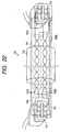
- a metal cable 150 conforming to the IEEE1394 standard typically has a 6-pin connector 154 (or alternatively a 4-pin connector) connected at both ends of a cable 152, as shown in Fig. 22 .
- Each pin of the connector 154 (in the order from the first pin to the sixth pin) is supplied with a power source (voltage) from an outside apparatus connected to the connector 154 and the GND to enable four signals of TPA, TPA*, TPB and TPB* to be input or output.
- a sign "*" denotes an inverse signal.
- TPA and TPA* are received and either one of them is used as the Data signal
- TPB and TPB* are received and either one of them is used as the Strobe signal.
- the STP is less sufficient to prevent signal deterioration due to the noise, the length of cable being limited to 4.5m, which means that the STP can not be employed for the long distance connection between the devices.
- the IEEE1394.b standard for optical transmission is about to be instituted to enable the connection between the remote sites by optically transmit ting or receiving the signal.
- This IEEE1394.b standard is intended for the bi-directional communications, employing two wires.
- the optical module examined above makes the bi-directional communication through the single wire line, it is necessary to have different light wavelengths for transmission and reception to improve the signal quality. This is required to decrease the cross talk of light. Therefore, the optical module has the higher cost.
- an optical transmission and reception module comprising electrical signal input/output means for inputting or outputting a first electrical signal and a second electrical signal relevant with the first electrical signal from or to the outside, conversion means for converting the first electrical signal and the second electrical signal into a first optical signal and a second optical signal, respectively, and inversely converting the first optical signal and the second optical signal into the first electrical signal and the second electrical signal, respectively, first optical signal input/output means for inputting or outputting the first optical signal from or to an optical transmission medium, and second optical signal input/output means for inputting or outputting the second optical signal from or to the same optical transmission medium as the first optical signal at a different wavelength from the first optical signal, wherein an optical waveguide transmission device included in said optical transmission and reception module is manufactured by a method including a mixing step for mixing a first photosetting resin comprising a first photopolymerization initiator and a first monomer or oligomer polymerized by a first polymerization mechanism by the first photopolymer
- the first and second electrical signals when transmitting a signal, are input from the outside by electrical signal input/output means, and converted into the first and second optical signals by the conversionmeans, respectively.
- the first optical signal is input into the optical transmission medium such as optical fiber by the first optical signal input/output means, and the second optical signal is made a different wavelength from the first optical signal and input into the same optical transmission medium for the first optical signal by the second optical signal input/output means, the first and second optical signals being transmitted through the same optical transmission medium.
- the first optical signal When receiving a signal, the first optical signal is output from the optical signal transmitted through the optical transmission medium by the first optical input/output means, and the second optical signal is output by the second optical signal input/output means. And the first and second optical signals output are inversely converted into the first and second electrical signals by the conversion means, respectively. Then, the first and second electrical signals are output to the outside by the electrical signal input/output means.
- the first and second electrical signals are converted into first and second optical signals having different wavelengths, respectively, and entered into the same optical transmission medium, while the first and second optical signals having different wavelengths transmitted through the optical transmission medium are inversely converted into the first and second electrical signals, respectively, and output to the outside.
- optical transmission and reception module is applicable for the connection between remote sites.
- the electrical signals are employed for the input or output from or to the outside, and are converted into the optical signals within the communication device, whereby there is no need of providing the special equipment for the communications between the devices employing the conventional metal cable, resulting in the reduced costs for using this communication device.
- the second optical signal input/output means preferably comprises synthesis and separation means for synthesizing two optical signals having different wavelengths that are output from the first optical signal input/output means and the second optical input/output means to input a synthesized signal into the optical transmission medium, and separating the two optical signals having different wavelengths transmitted through the optical transmission medium.
- the secondoptical signal input/outputmeans uses the synthesis and separation means to synthesize the first and second optical signals having different wavelengths to enter a synthesized signal into the optical transmission medium, when transmitting a signal, while separating a signal transmitted through the optical transmission medium into the first and second optical signals, when receiving the signal.
- the communications of the first and second optical signals via the same optical transmission medium can be simply provided.
- Such synthesis and separation means can be implemented by employing a wavelength filter, for example.
- the optical transmission and reception module further comprising guide and separation means for guiding an optical signal for input into the optical transmission medium to the optical transmission medium, and separating an optical signal for output from the optical transmission medium, the guide and separation means being provided on at least one of the first optical signal input/output means and the second optical signal input/output means.
- the guide and separation means provided at least one of the first and second optical signal input/output means can guide an optical signal for input into the optical transmission medium from the corresponding optical signal input/output means into the optical transmission medium, when transmitting the signal, or separates the optical signal for output from the optical signal medium to output the signal, when receiving the signal.
- the electrical signal conforms to the IEEE1394 standard.
- the optical transmission medium preferably can be employed as a substitute for the 1394 standard metal cable, because the electrical signals (first and second electrical signals) conform to the IEEE1394 standard.
- the optical transmission and reception module preferably comprises connection means for connecting the optical signal to the optical transmission medium so that the optical signal can be input or output from or to the optical transmission medium.
- a communication device in which the optical transmission and reception module is preferably provided at either end of the optical transmission medium.
- the optical transmission medium can be simply employed as a substitute for the conventional metal cable, because the optical transmission and reception module is provided at either end of the optical transmission medium, and integrally formed.
- the photosetting resin solution is filled in the space area for forming the optical transmission device within the optical transmission and reception module, and one end of the optical fiber is inserted through the light input/output opening of the optical transmission and reception module, and then the light emitting elements are caused to emit light.
- the light beam of predetermined wavelength for communication is passed through a predetermined path within the optical transmission and reception module to proceed toward the light input/output opening to be incident upon one end face of the optical fiber, and output via the optical fiber to the outside of the optical transmission and reception module.
- the light input/output axis direction of the optical fiber is adjusted so that the quantity of output light is almost at maximum, while detecting the quantity of output light.
- a light beam of predetermined wavelength for formation of optical transmission device is entered from the other end of the optical fiber to the optical transmission and reception module, while maintaining the adjusted light input/output axis direction of the optical fiber, so that the light beam for formation of the optical transmission device is introduced into the photosetting resin solution to form the optical transmission device, whereby the light beam can be transmitted at almost maximum efficiency in the optical transmission device formed. Accordingly, it is possible to omit the operation of making the alignment of the optical axis of the light emitting or receiving element in the optical transmission and reception module with respect to the optical transmission device formed.
- the optical transmission device within the optical transmission and reception module according to the present invention is produced in a state where one end of the optical fiber is immersed in the photosetting resin solution.
- the optical transmission device within the optical transmission and reception module according to the present invention is formed in a state of connecting it with one end of the optical fiber, and the optical fiber is fixed by the formed optical transmission device, without causing misalignment between the optical fiber and the optical transmission device that are coupled.
- the optical transmission device is internally formed within the optical transmission and reception module according to the present invention by the above method, the optical beam can be transmitted at almost maximum efficiency without making the alignment of optical axes for the light emitting and receiving elements after forming the optical transmission device. That is, the optical transmission and reception module with less optical loss and that is efficient can be produced simply.
- optical transmission and reception module two relevant electrical signals (first electrical signal and second electrical signal) input from the outside are transmitted simultaneously, converted into the optical signals having different wavelengths (first optical signal and second optical signal) by the conversion means, and entered into the same optical fiber by the first optical signal input/output means and the secondoptical signal input/output means. Also, the optical signals having different wavelengths (first optical signal and second optical signal) transmitted via the optical fiber are inversely converted into the electrical signals (first electrical signal and second electrical signal) and output to the outside.
- the optical transmission and reception module can be employed for the communication conforming to the IEEE1394 standard.
- the electrical signals are input or output from or to the outside, and converted into the optical signals within the communication device. Therefore, the optical transmission and reception module can be applied to the communications between the devices employing the conventional metal cable, without needing any special equipment, and can be utilized without increasing the costs.
- the optical transmission and reception module preferably comprises the light propagating means having the optical transmission device formed by the above method for forming the optical transmission device according to the invention between the optical fiber and the first optical signal input/output means, and between the optical fiber and the second optical signal input/output means, whereby the first and second optical signals can be input or output from or into the optical fiber efficiently by the light propagating means and transmitted or received via the optical fiber to or from the outside.
- Pig-Tail type in which the other end of the optical fiber is extended a predetermined length from the housing of the optical transmission and reception module for the connection with the external apparatus.
- the second optical signal input/output means comprises synthesis and separation means for synthesizing two optical signals having different wavelengths that are output from the first optical signal input/output means and the second optical signal input/output means to enter a synthesized signal into the optical fiber, and separating two optical signals having different wavelengths that are transmitted through the optical fiber.
- the second optical signal input/output means comprises the synthesis and separation means to synthesize the first optical signal and the second optical signal that have different wavelengths to be input into the optical fiber, when transmitting the signal, or separate the synthesized signal transmitted through the optical fiber into the first optical signal and the second optical signal in receiving the signal. Accordingly, the communications of the first optical signal and the second optical signal via the same optical fiber can be simply provided.
- This synthesis and separation means can be implemented employing the wavelength filter, for example.
- the above optical transmission and reception module preferably further comprises guide and separation means for guiding an optical signal for input into the optical fiber to a light transmission medium and separating an optical signal for output from the optical fiber, the guide and separation means being provided on at least one of the first optical signal input/output means and the second optical signal input/output means.
- the optical signal for input into the optical fiber that is passed from the corresponding optical signal input/output means is guided into the optical fiber, when transmitting the signal, or the optical signal for output from the optical fiber is separated and output (received) , when receiving the signal. Accordingly, the optical signal for input can be entered into the optical fiber efficiently, and the optical signal for output from the light transmission medium can be received efficiently by the output section, reducing the optical loss (LOSS).
- the monomers for effecting radical photopolymerization preferably include (meth)acrylic ester and (meth)amide acrylate.
- one functional (meth)acrylic ester can be employed, such as (meth) acrylate 2-ethylhexyl, (meth)acrylate cyclohexyl, and (meth)acrylate 2-butoxyethyl.
- ester (di(meth)acrylate) between diol such as ethylene glycol, neopentyl glycol, or 1, 6-hexanediol, and 2 isosteric(meth)acrylic acid can be employed.
- ester (tri, tetra, ..., (meth) acrylate) between organic compound having alcohol hydroxyl groups and (meth) acrylic acid can be also employed.
- (meth) acryloyl radical and other organic skeleton methyl hydrogen, methylene hydrogen, or methyne hydrogen partially substituted by halogen may be employed.
- oligomer for effecting radical photopolymerization
- urethane oligomer polyether oligomer, epoxy oligomer, and polyester oligomer having (metha) acryloyl radical at the termination or branch are preferable.
- (meth) acryloyl radical and other organic skeleton methyl hydrogen, methylene hydrogen, or methyne hydrogen partially substituted may be employed.
- radical photopolymerization initiator examples include benzyldimethylketal compounds including 2, 2-dimethoxy-2-phenylacetophenone, ⁇ -hydroxyketone compounds including 2-hydroxy-2-methyl-phenylpropane-1-one, and (1-hydroxycyclohexyl)-phenylketone, ⁇ -aminoketone compounds including 2-benzyl-2-dimethylamino-1-(4-morpholinophenyl)-butane-1-on, 2-methyl-1-(4-(methylthio)phenyl)-2-morpholinopropane-1-one, bisacylphosphineoxide compounds including bis(2, 6-dimethoxybenzoyl-2, 4, 4-trimethyl-pentylphosphineoxide, bis(2, 4, 6-trimethylbenzoyl)-phenylphosphineoxide, metallocene compounds - including bis( ⁇ -cyclopentadienyl)-bis(2, 6-difluoro-3- (N-pyroyl)
- Examples of the monomer or oligomer for effecting cationic photopolymerization include epoxy ring, oxetane ring, cyclic ether compound, cyclic lactone compound, cyclic acetal compound, and vinyl ether compound.
- Examples of the cationic photopolymerization initiator include 4, 4'-bis(di(2-hydroxyethoxy) phenylsulfonio) phenylsulfidedihexyfluoroantimonate, and ⁇ -cyclopentadienyl- ⁇ -cumene iron(1+)-hexafluorophosphoric acid(1-).
- Fig. 1 shows a method for manufacturing an optical transmission device in a first example.
- An optical fiber 1, a mixture solution (photosetting liquid resin composition) 2 of the photosetting resins 21 and 22 polymerizing in two different polymerization types, and a transparent container 3 were prepared.
- the product number 358 (hereinafter referred to simply as a resin A) manufactured by Loctite Inc. to make radical photopolymerization
- the product number UV-2100 hereinafter referred to simply as a resin B) manufactured by Dykin Inc. to make cationic photopolymerization were employed.
- the truncated cone and the spheroid are employed.
- the structure may be constructed by the wall face of any polyhedron or any curved surface.
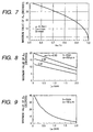
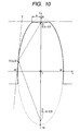
- the structure not only expands from the terminal area to the point of notice, as will be apparent from Fig. 10 , but also may be a curved surface or polyhedron having a narrowed portion.
- th-is structure may take a shape of an inverse truncated cone as a whole or partially.
- a communication cable 310 for a communication device of the present invention has an optical transmission and reception module 314 connected to either end of an optical fiber 312 as an optical transmission medium, as shown in Fig. 11 .
- the input/output module 316 has two pairs of light emitting elements (LD) 322 and light receiving elements (PD) 324 as first and second optical signal input/output means.
- LD light emitting elements
- PD light receiving elements
- one pair is referred to as a light emitting element 322A and a light receiving element 324A
- the other pair is referred to as a light emitting element 322B and a light receiving element 324B.
- the beam splitters 326A, 326B are disposed as guide means, respectively.
- the beam splitters 326A, 326B transmit a predetermined quantity of light and reflect a predetermined quantity of light among the light beams LA, LB, so that the transmitted light quantity and the reflected light quantity may be at a certain division ratio (e.g., 1: 1) .
- the beam splitters 326A, 326B may have a function of deflecting optics such as a deflecting beam splitter to regulate the ratio between the transmitted light and the reflected light at will.
- the light beams LA and LB are reflected at a predetermined quantity of light, for example, at a division ratio of 1:1, by the beam splitters 326A and 326B, and guided toward the light receiving elements 324A and 324B to be incident upon the light receiving plane of the light receiving elements 324A and 324B.
- both or one of the light receiving elements may be arranged side by side with the light emitting elements to be paired in accordance with, for example, the output light quantity of the light emitting element or the significance of the transmitting signal, thereby omitting the beam splitters.
- the connector 318 is connectable to the input/output terminal on the side of the external device to enable an electric signal to be input or output from or to the external device.
- Each pin of the connector 318 is connected to the driving and processing circuit 320, which is connected to the light emitting elements 322A, 322B and the light receiving elements 324A, 324B for the input/output module 316.
- the communication cable 310 is employed to connect a digital video camera to a digital video deck, when dubbing a video picked up by the video camera in the digital video deck, for example.
- the digital video camera is connected to the digital video deck via the communication cable 310 by fitting the connector 318 provided in the transmission and reception module 314 at one end of the communication cable 310 into a terminal according to IEEE1394 standard provided in the digital video camera, and the connector 318 provided in the transmission and reception module 314 at the other end of the communication cable 310 into a terminal according to IEEE1394 standard provided in the digital video camera.
- the electric signals TPA and TPA* as the Data signal and TPB and TPB* as the Strobe signal are output from the external apparatus on the signal transmission side, and input via the connector 318 connected to the external apparatus into the transmission and reception module 314, as shown in Fig.12 .
- an electric power supplied via the connector 318 from the external apparatus on the signal transmission side to the transmission and reception module 314, placing the transmission and reception module 314 in operable state.
- the transmission and reception module 314 on the side where the electrical signals are input from the external apparatus is referred to as the transmission side
- the transmission and reception module 314 on the other side is referred to as the receiving side.
- the electric signals passed from the external apparatus into the transmission and reception module 314 on the transmission side are input into the driving and processing circuit 320, which then generates the lighting signals for Data signal and Strobe signal, on the basis of the input electric signals.
- a lighting signal for Data signal is generated on the basis of either one of the TPA and TPA* signals
- a lighting signal for Strobe signal is generated on the basis of either one of the TPB and TPB* signals.
- the driving and processing circuit 320 controls the driving of the light emitting element 322B of the input/output module 316 on the basis of the generated lighting signal for Strobe signal to output a light beamLB corresponding to the Strobe signal from the light emitting element 322B.
- the Strobe signal is output as an optical signal (Strobe light signal) from the light emitting element 322B.
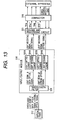
- the synthesized light beam LC transmitted through the optical fiber 312 is output from the other end face, and then input into the input/output module 316 of the transmission and reception module 314 on the receiving side, as shown in Fig. 13 .
- the synthesized light beam LC output from the other end face of the optical fiber 312 is input into the input/output module 316 to be firstly incident upon the wavelength filter 328.
- the light receiving element324A receives the light beam LA incident upon the light receiving plane, an electric signal according to the received light quantity as a light receiving signal being output to the driving and processing circuit320.
- the light receiving element324B receives the light beam LB incident upon the light receiving plane, an electric signal according to the received light quantity as a light receiving signal being output to the driving and processing circuit 320.
- a value of the light receiving signal from the light receiving element 324A is compared with the threshold value, a binary signal of 0 or 1 is generated as the TPA (or TPB) signal in accordance with its comparison result, and the value of 1 or 0 of the TPA signal is inverted to generate the TPA* (TPB*) signal.
- the Data signal and the Strobe signal that are transmitted as the optical signal via the optical fiber 312 from the input/output unit on the transmission side are converted into the electric signals, respectively.
- the conversion from the optical signal into the electric signal is referred to as an "inverse conversion" with respect to the conversion from the electric signal into the optical signal.
- the driving and processing circuit 320 outputs the generated TPA, TPA*, TPB and TPB* signals via the connector 318 to the external apparatus on the receiving side connected to the connector 318.
- the signals are optically transmitted, thereby eliminating the fear for the noise caused by electromagnetic induction that brought about the problem in STP.
- the limited length of cable can be relieved, and the cable can be extended over 50m, for example, as compared with the conventional 1394 standard metal cable.
- onlyone optical fiber 312 enables the simultaneous transmission of two signals (Data signal and Strobe signal) , resulting in lower costs.
- the synthesis of two signals on the transmission side and the separation of two synthesized signals on the reception side can be easily implemented by employing the wavelength filter 328.
- the beam splitters 326A, 326B guide the light beams LA, LB output from the light emitting elements 322A, 322B toward the wavelength filter 328 to enter the optical fiber via the wavelength filter 328 on the transmission side, and guide the light beams LA, LB separated by the wavelength filter 328 to the light receiving elements 324A, 324B on the reception side, whereby the light beams LA, LB output from the light emitting elements 322A, 322B on the transmission side are received by the light receiving elements 324A, 324B on the reception side with less optical loss.
- the transmission and reception module 314 does not require any optical parts, viz., can be constructed by so-called bulk products for the wavelength filter 328, the beam splitters 326, the light emitting elements 322, and the light receiving elements 324, with reduced costs.
- the communication cable 310 has the optical fiber 312 and the transmission and reception module 314 integrated.
- the invention is not limited to this embodiment, but the transmission and reception module 314 may be formed apart from the optical fiber 312.
- a plug 330 is formed by working both ends of the optical fiber 312 (only one end shown in Fig. 14 ), and a socket 332 as connecting means is formed by working the input/output module 316 of the transmission and reception module 314, thereby fabricating an optical connector, as shown in Fig. 14 .
- the plug 330 is fitted into the socket 332, so that the optical fiber 312 and the transmission and reception module 314 are connected, as indicated by the arrow A.
- the above transmission and reception module 314 has a structure almost the same as that of an optical transmission and reception module 410 hereinafter described shown in Fig. 21 .
- an optical transmission device can be manufactured within the transmission and reception module 314 according to a manner same as the first to third examples.
- an optical transmission and reception module 410 comprises internally a light emitting element 412 such as an LD (Laser Diode) and a light receiving element 414 such as a PD (Photo Diode) , and a housing 416 has an input/output opening 416A for inputting or outputting a light beam from or into the outside.
- the optical transmission and reception module 410 guides a light beamLB1 output from the light emitting element 412 via an optical member such as a beam splitter or a mirror into the input/output opening 416A, and guides a light beam input through the input/output opening416A into the optical transmission and reception module 410 via the optical member to the light receiving element 414.
- One end 418A (hereinafter referred to as an "endportion") of an optical fiber 418 is inserted through this input/output opening 416A, with the other end 418B (hereinafter referred to as "end portion") left outside the housing 416, whereby an optical transmission device 450 (see Fig. 18 ) for optically coupling the optical fiber 418 with the light emitting element 412 and the light receiving element 414 in a spatial area between the end portion 418A of the optical fiber 418 and the light emitting element 412 and the light receiving element 414 by employing an optical-transmission-device self-forming apparatus 420 as will be described later.
- an optical transmission device 450 see Fig. 18
- the optical-transmission-device self-forming apparatus 420 comprises an optical-transmission-device forming light source 422, a photo-detector 424 for detecting the light, such as PD, an optical directional coupler 426, an optical connector module 428 for connecting the end portion 418B of the optical fiber 418 to the optical directional coupler 426, and a mixture solution 430 composed of two sorts of photosetting resin solutions having different setting start wavelengths and the different refractive indexes after hardening, which is filled into the housing 416 (i.e., the spatial area for forming the optical transmission device 450) in forming the optical transmission device 450, as shown in Fig. 16 .
- theoptical transmission device 450 is formed by a basically same manner as the first to third examples.
- the optical-transmission-device forming light source 422 comprises two sorts of light sources for outputting the light having different wavelengths, more specifically, a short wavelength laser 422A for hardening one component of the mixture solution linearly and a ultraviolet lamp 422B for hardening the mixture solution 430 as a whole.
- the light beam output from the short wavelength laser422A is hereinafter referred to as the light beam LB2.
- the optical directional coupler 426 optically couples the optical fiber 418 connected via the optical connector module 428 with the short wavelength laser 422A and the photo-detector 424, and guides all or part of the light beam proceeding from the optical fiber 418 to the short wavelength laser 422A in accordance with a predetermined division ratio to the photo-detector 424.
- the photo-detector 424 receives this light beam and monitors the quantity of output light from the optical fiber 418.
- the light beam LB1 output via the optical fiber 418 from the optical transmission and reception module 410 is led to the photo-detector 424, and the light beam LB2 output from the short wavelength laser 422A is introduced via the optical fiber 18 into the optical transmission and reception module 410. Also, owing to rectilinear propagation of the light beam, the paths of the light beams LB1 and LB2, viz., the optical axes of both light beams in both directions within the optical transmission and reception module 410 are almost coincident.
- a beam splitter may be employed to obtain the same effect.
- the mixture solution 430 is composed of, for example, an epoxy-based, high refractive index photosetting resin solution with a refractive index of 1.49, and an acrylic, low refractiveindex photosetting resinsolution with a refractive index of 1.34.
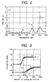
- the spectral sensitivity characteristics for both solutions are shown in Fig. 17 .
- the transverse axis indicates the wavelength and the longitudinal axis indicates the relative sensitivity.
- a curve A is a spectral sensitivity characteristic for epoxy-based, high refractive index photosetting resin solution
- a curve B is a spectral sensitivity characteristic for acrylic, low refractive index photosetting resin solution.
- respective setting start wavelengths are selected to occur across the wavelength ⁇ 1 of the light beam LB2 output from the short wavelength laser 402A used for hardening. Also, respective setting start wavelengths are selected to be shorter than the wavelength of the light beam transmitted and received by the optical transmission and reception module 410, so that none of the photosetting resin solutions are hardened by the light beam LB1 output from the light emitting element 412. Since the photosetting resin solution is not hardened at a moment, the light beams LB1 and LB2 can be made the same wavelength. However, it is preferable that the wavelength of light beam LB1 or the sensitivity of solution is set so that the wavelength of light beam LB1 may not have influence on the hardening of the photosetting resin solution.
- solution A the high refractive index photosetting resin solution
- solution B the low refractive index photosetting resin solution
- the refractive index n c1 of the mixture solution is represented in the expression (17) (refer to Yamaguchi, "Refractive Index” publishedbykyoritsu (1982).
- p is the concentration of mixture solution
- ⁇ A is the concentration of solution A
- ⁇ B is the concentration of solution B
- n A1 is the refractive index of solution A
- n B1 is the refractive index of solution B
- C A is weight percent of solution A.
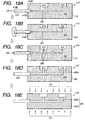
- the mixture solution 430 is filled in the housing 430 of the optical transmission and reception module 410, and the endportion 418A of the optical fiber 418 is inserted through the input/output opening 416A of the optical transmission and reception module 410 to have its tip end immersed in the mixture solution 430, as shown in Fig. 18A .
- the light emitting element 412 is lighted to direct a light beam into the mixture solution that is filled in an area for forming the optical transmission device 450.
- the mixture solution 430 is filled in the overall housing 416, but the mixture solution 430 may be filled in at least a spatial area for forming the optical transmission device 450 within the housing 416 of the optical transmission and reception module 410, more specifically in an area between the light emitting element 412 and the input/output opening 416A.
- the photo-detector 424 outputs a signal in accordance with the quantity of detected light (hereinafter referred to as a "light quantity signal”) .
- a light quantity signal the quantity of light output via the optical fiber 418 to the outside among the light beam LB1 output from the light emitting element 412 can be grasped.
- the optical fiber 418 is moved in the X-Y direction, while monitoring the light quantity signal output from this photo-detector 424 as shown in Fig. 18B and Fig. 19 .
- the optical fiber 418 has its axial direction changed with respect to a fixed point that is the position substantially coincident with the input/output opening 416A, so that the light input or output direction (axial direction for inputting or outputting the light) of the optical fiber 418 with respect to the optical transmission and reception module 410 is changed.
- the quantity of light incident upon the optical fiber 418, among the light beam LB1 output from the light emitting element 412 is changed, and therefore the quantity of light detected by the photo-detector 424 is changed.
- the position of the optical fiber 418 is adjusted to the position at which the quantity of detected light is at maximum as indicated by the light quantity signal. If this adjustment is made, the light emitting element 412 is turned off.
- the short wavelength laser 422A is lighted to enable the light beam LB2 to enter the mixture solution 430 in a state where the position of the optical fiber 418 after adjustment is maintained, as shown in Fig. 18C and Fig. 19 .
- the light beam LB2 output from the short wavelength laser 422A is incident upon the end face at the end portion 418B of the optical fiber 418 via the optical directional coupler 426 and the optical connector module 428.
- the light beam LB2 incident upon the end face at the end portion 418B is transmitted through the optical fiber 418, and output from the end face at the end portion 418A into the mixture solution 430 filled within the optical transmission and reception module 410.
- the light beam LB2 output from the optical fiber 418 is passed almost inversely through the transmission line of the optical beam LB1 after adjustment in the mixture solution 430 to travel toward the light emitting element 412.
- the optical axis of the light beam LB2 is substantially the same as the light beamLB1 after adjustment.
- the light beam entered through the input/output opening 416A inwards is branched into the light receiving element 414 by the beam splitter, and received by the light receiving element 414 to receive an optical signal, whereby a part of the light beam LB2 is also branched to travel toward the light receiving element 414.
- the short wavelength laser 422A is a He-Cd (helium Cadmium) laser having a wavelength ⁇ 1 of 325nm, for example.
- This wavelength is shorter than the setting start wavelength of solution A, and longer than that of solution B, as mentioned above. Accordingly, the solution A is only hardened. Also, with the light beam rays, the light beam LB2 can propagate almost rectilinearly.
- a linear core portion 450A optical transmission line
- the solution B on the optical axis is forced aside.
- a ultraviolet ray UV having wavelength ⁇ 2 is radiated uniformly from around the core portion 450A by a ultraviolet lamp422B, as shown in Fig. 18E .
- This wavelength ⁇ 2 is shorter than the setting start wavelengths of the solutions A and B, whereby the solutions A and B can be both hardened, as shown in Fig. 17 .
- the surroundings of the core portion 450A viz., the entire mixture solution 430, can be hardened to form a clad portion 450B and produce the optical transmission device 450. Consequently, the tip end (endportion 418A) of the optical fiber 418 and the light emitting element 412 and the light receiving element 414 are coupled with the optical transmission device 450.
- the refractive index n A2 of the core portion 450A satisfies the following expression (18). n A ⁇ 2 > n C ⁇ 2 > n C ⁇ 1
- the light transmission line is a step index type in which the refractive index n A2 of the core portion 450A is higher than the refractive index n C2 of the clad portion 450B. Accordingly, other light beam introduced into the optical transmission device 450 or other light beam introduced at an angle meeting the total reflection condition as will be described later propagates, while being totally reflected through the core portion 450A of the optical transmission device 450.
- the mixture solution 430 is filled in the area for forming the optical transmission device 450 within the light transmission module 410, and the optical fiber 418 having the end portion 418A inserted into the optical transmission and reception module 410 through the light input/output opening 416A is optically coupled with the short wavelength laser 422 and the photo-detector 424, as shown in Fig. 19 . Then the light beam LB1 is output from the light emitting element 412, and the optical fiber 418 is moved in the X-Y direction, so that the light quantity of the light beam LB1 output via the optical fiber 418 to the outside may be almost at maximum.
- the short wavelength laser 422A is lighted to form the core portion 450A.
- a ultraviolet ray UV from the ultraviolet lamp 422B is directed over the mixture solution 430 to form the clad portion 450B.
- the optical transmission device 450 is formed between the tip end of the optical fiber 418 and the light emitting element 412 and the light receiving element 414.
- the formed optical transmission device 450 can transmit the light beam at almost maximum efficiency to the optical transmission and reception module 410. That is, it is unnecessary for the formed optical transmission device 450 to adjust the optical axis of the light emitting element 412 or the light receiving element 414 within the optical transmission and reception module 410, resulting in optical loss inside. That is, it is possible to produce the optical transmission and reception module 410 that can transmit and receive the optical signal efficiently.
- the optical transmission device 450 can be formed in a state where the tip end (18A) of the optical fiber 418 is immersed in the mixture solution 430, thereby securing the optical fiber 418 by means of the clad portion 450B formed. Thereby, it is possible to produce simply a so-called Pig-Tail type device in which the optical fiber 418 is formed integrally with the optical transmission and reception module 410 in a state where the other end 418B of the optical fiber 418 is extended from the housing 416.
- the optical fiber 418 for each optical transmission and reception module 410 may be connected by the optical connector 454, as shown in Fig. 20 . Also, when the optical telecommunications are performed, if another optical fiber 460 is connected between the optical fibers 418 for the optical transmission and reception modules 410 by the optical connector 454, the communication distance can be simply extended. Also, the length of the optical fiber 418 extending from the housing 416 may be as short as about 10cm, because the optical fiber can be extended easily.
- the optical transmission and reception module 410 may be in any form, so long as it can transmit or receive the optical signal to or from the outside.
- An example of the optical transmission and reception module will be set forth below which can transmit and receive two sorts of optical signals at the same time employing two light beams having different wavelengths.
- the optical transmission and reception module 410 as shown in Fig. 21 has the same structure as that of the optical transmission and reception module 314. It comprises an input/output module 440 for inputting or outputting an optical signal from or to the end face of the optical fiber 418, a connector 442 as electrical signal input/output means connected to an external apparatus to make the input or output of an electrical signal from or to the external apparatus, and a driving/processing circuit 444 as conversion means.
- the housing of the input/output module 440 is formed with an opening 440A, in which an optical guide 450 is formed by inserting one end portion 418A of the optical fiber 418 through the light input/output opening 416A of the housing 416 for the light transmission/reception module 410 itself into the opening 440A.
- the input/output module 440 comprises two pairs of light emitting elements 412 and light receiving elements 414 as first and second optical signal input/output means.
- one pair is a light emitting element 412A and a light receiving element 414A
- the other pair is a light emitting element 412B and a light receiving element 414B.
- the light emitting elements 412A and 12B output light beams having different wavelengths ⁇ 3 and ⁇ 4, respectively. Specifically, the light emitting element 412A outputs a light beams having a wavelength ⁇ 3 of 650nm and the light emitting element 412B outputs a light beams having a wavelength ⁇ 4 of 520nm in this embodiment. This is because the typical POF has the wavelength band (so-called window) having low optical loss at a wavelength of 650nm and in a range of wavelength from 470 to 550nm.
- the light receiving elements 414A and 414B receives a light beam incident upon the light receiving plane, and output an electrical signal in accordance with the received quantity of light.
- This electrical signal is hereinafter referred to as a light receiving signal.
- the beam splitters 44 6A, 446B are placed as guiding means in a traveling direction of the light beam output from the light receiving elements 412A and 412B.
- the beam splitters 446A, 446B transmit a predetermined quantity of light among the light beam and reflect a predetermined quantity of light so that the transmitted light quantity and the reflected light quantity may be at a certain division ration (e.g., division ration of 1:1).
- the beam splitters 446A, 446B may have a deflecting optical function of the deflecting beam splitter to regulate the ratio between the transmitted light and the reflected light at will.
- awavelength filter 448 as synthesis/separation means for transmitting the light beam having a predetermined wavelength and the light beam having another predetermined wavelength is placed. More particularly, the wavelength filter 448 transmits the light beam having wavelength ⁇ 3 and reflects the light beam having wavelength ⁇ 4 to synthesize two light beams having different wavelengths that are output from the light emitting elements 412A, 412B.
- the wavelength filter 448 will function as a half mirror in other wavelength bands.
- the light beam synthesized by this wavelength filter 448 is incident upon the end face at the end portion 418A of the optical fiber 418 inserted into the opening 440A, transmitted through the optical fiber 418 toward the end portion 418B and output from the end face at the end portion 418B.
- a condenser lens may be disposed to condense the light beam to enter the optical fiber 418, or for example, a collimator lens is disposed to make the light beam parallel, so that the light beam may be incident upon the optical fiber 418 to be parallel to the optical axis of the optical fiber 418, thereby reducing the optical loss on the end face of the optical fiber 418.
- the light beam having wavelength ⁇ 3 and the light beam having wavelength ⁇ 4 are reflected by predetermined quantities of light by the beam splitters 446A and 446B, for example, at a division ratio of 1:1, respectively, and guided toward the light receiving elements 414A and 414B to be incident upon the light receiving planes of the light receiving elements 414A and 414B, respectively.
- both or one of the light receiving elements may be arranged side by side with the light emitting elements to be paired in accordance with, for example, the output light quantity of the light emitting element or the significance of the transmitting signal, thereby omitting the beam splitters.
- the connector 442 has four pins for inputting or outputting a total of four signals, including two electrical signals of TPA and TPA* as the Data signal and two electrical signals of TPB and TPB* as the Strobe signal, from or to the external apparatus, and two pins for receiving a power supply for driving the transmission and reception module 410 and the GND from the external apparatus, or six pins in total (a so-called 6-pin connector).
- a 4-pin connector may be employed by omitting the pins for the power supply and the GND.
- the IEEE1394 standard is exemplified, but the invention is not limited to the IEEE1394 standard. Besides the IEEE1394 standard, the GPIB or RS232C standard may be also employed.
- Each pin of the connector 442 is connected to the driving and processing circuit 444, which is then connected to the light emitting elements 412A, 412B and the light receiving elements 414A, 414B for the input/output module 440.
- the driving and processing circuit 444 has each signal of TPA, TPA*, TPB and TPB* input via the connector 442 from the external apparatus.
- the driving and processing circuit 444 generates a lighting signal for the Data signal and a lighting signal for the Strobe signal, on the basis of an electrical signal input from the external apparatus, and controls the driving of the light emitting elements 412A, 412B, on the basis of the lighting signal for the Data signal and the lighting signal for the Strobe signal that are generated.
- the driving and processing circuit 444 has a light receiving signal input from the light receiving elements 14A, 14B.
- the driving andprocessing circuit 444 processes the light receiving signal from the light receiving elements 414A, 414B to generates each signal of TPA, TPA*, TPB and TPB*, and output it via the connector 442 to the external apparatus connected to the connector 442.
- the transmission and receptionmodule 410 employs a power supply via the connector 442 from the external apparatus to drive the driving and processing circuit 444, the light emitting elements 412 and the light receiving elements414.
- the mixture solution 430 is filled in the input/output module 440, the end portion 418A of the optical fiber 418 is passed through the input/output opening 416A of the optical transmission and reception module 410 into the opening 440A of the input/output module 440, and the tip end at the end portion 418A is immersed in the mixture solution 430, for example.
- the light emitting elements 412A and 412B are lighted, a predetermined quantity of light among the light beam output from the light emitting element 412A is transmitted through the beam splitter 46A to be incident upon the wavelength filter 448.
- the short wavelength laser 422A is lighted while maintaining the state after adjustment.
- the light beam LB2 output from the short wavelength laser 422A is incident upon the end face of the optical fiber 418B and transmitted through the optical fiber 418 to be output from the end face of the optical fiber 418A into the mixture solution 440 filled within the light input/output module 440. And first of all, the light beam is incident upon the wavelength filter 448, which transmits a part of the light beam and reflects its other part because it operates as a half mirror for the light beam LB2.
- the light beam LB2 is divided into the directions toward the light emitting elements 412A and 412B by the wavelength filter 4448, a predetermined quantity of light among the part of the light beam LB2 traveling in the direction toward the light emitting element 412A is transmitted through the beam splitter 446A to travel to the light emitting element 412A, and the remaining quantity of light is reflected by the beam splitter 446A and guided in the direction toward the light receiving element 414A.
- a predetermined quantity of light among the other part of the light beam LB2 traveling in the direction toward the light emitting element 412B is transmitted through the beam splitter 446B to travel directly to the light emitting element 412B, and the remaining quantity of light is reflected by the beam splitter 446B and guided in the direction toward the light receiving element 414B.
- the light beam LB2 output from the short wavelength laser 422A is divided into the directions toward the light emitting elements 412A, 412B and the light receiving elements 414A, 414B by the wavelength filter 448, and the beam splitters 446A and 446B, whereby the core portion 450A (optical transmission line) is formed in the mixture-solution 430 to be branch from the end portion 418A of the optical fiber 418 into the light emitting elements 412A, 412B and the light receiving elements 414A, 414B.
- the ultraviolet lamp 422B is lighted to direct ultraviolet rays UV from around the mixture solution 430 to harden the entire mixture solution 430, thereby forming the clad portion 450B.
- theopticaltransmissiondevice 450 can be formed to couple the optical fiber 418 with the light emitting elements 412A, 412B and the light receiving elements 414A, 414B between the tip end of the optical fiber 418 and the light emitting elements 412A, 412B and the light receiving elements 414A, 414B.
Landscapes
- Physics & Mathematics (AREA)
- General Physics & Mathematics (AREA)
- Optics & Photonics (AREA)
- Engineering & Computer Science (AREA)
- Microelectronics & Electronic Packaging (AREA)
- Optical Couplings Of Light Guides (AREA)
- Optical Integrated Circuits (AREA)
Claims (6)
- Optisches Übertragungs- und Empfangsmodul (314), umfassend:elektrische Signaleingabe/ausgabemittel (318) zum Eingeben oder Ausgeben eines ersten elektrischen Signals und eines zweiten elektrischen Signals, das bezüglich des ersten elektrischen Signals relevant ist, von außen oder nach außen,Umwandlungsmittel zum Umwandeln des ersten elektrischen Signals und des zweiten elektrischen Signals in ein erstes optisches Signal bzw. ein zweites optisches Signal, und umgekehrt zum Umwandeln des ersten optischen Signals und des zweiten optischen Signals in das erste elektrische Signal bzw. das zweite elektrische Signal,erstes optisches Signal-Eingabe/Ausgabemittel (322A, 324A) zum Eingeben oder Ausgeben des ersten optischen Signals von oder zu einem optischen Übertragungsmedium, undzweites optisches Signal-Eingabe/Ausgabemittel (322B, 324B) zum Eingeben oder Ausgeben des zweiten optischen Signals von oder zu dem gleichen optischen Übertragungsmedium wie bei dem ersten optischen Signal bei einer Wellenlänge, die von derjenigen des ersten optischen Signals verschieden ist,wobei eine Lichtwellenleiterübertragungsvorrichtung, die in dem optischen Übertragungs- und Empfangsmodul (314) enthalten ist, mit einem Verfahren hergestellt wird, das die Schritte umfasst:Mischen eines ersten lichthärtenden Harzes (21), das einen ersten Photopolymerisationsinitiator und ein erstes Monomer oder Oligomer umfasst, das durch einen ersten Polymerisationsmechanismus durch den ersten Photopolymerisationsinitiator polymerisiert wird, und eines zweiten lichthärtenden Harzes (22), das einen zweiten Photopolymerisationsinitiator und ein zweites Monomer oder Oligomer umfasst, das durch einen zweiten Polymerisationsmechanismus, der von dem ersten Polymerisationsmechanismus verschieden ist, durch den zweiten Photopolymerisationsinitiator polymerisiert wird, wobei die Polymerisation des ersten lichthärtenden Harzes einen Anstieg von dessen Brechungsindex verursacht,Bilden eines Kernabschnitts der Lichtwellenleiterübertragungsvorrichtung durch Härten des ersten lichthärtenden Harzes (21) durch Erzeugen einer ersten Bestrahlung von einem Wellenleiter, die den ersten Photopolymerisationsinitiator aktiviert, jedoch nicht den zweiten Photopolymerisationsinitiator aktiviert, undBilden eines Hüllenabschnitts der Lichtwellenleiterübertragungsvorrichtung durch Härten sowohl des ersten lichthärtenden Harzes (21) als auch des zweiten lichthärtenden Harzes (22) durch Erzeugen einer zweiten Bestrahlung, die sowohl den ersten Photopolymerisationsinitiator als auch den zweiten Photopolymerisationsinitiator aktiviert,wobei die erste Bestrahlung eine Wellenlänge aufweist, die kürzer ist als die längste Wellenlänge, die zur Aktivierung der ersten Photopolymerisation erforderlich ist, und länger ist als die längste Wellenlänge, die zur Aktivierung der zweiten Photopolymerisation erforderlich ist,wobei das optische Übertragungs- und Empfangsmodul (314) intern ein lichtemittierendes Element (322) zum Emittieren eines Lichtstrahls für eine Kommunikation mit einer vorgegebenen Wellenlänge und ein Lichtempfangselement (324) zum Empfangen des Lichtstrahls aufweist,wobei der Schritt des Bildens eines Kernabschnitts die Schritte desEinführens eines Lichtstrahls mit einer vorgegebenen Wellenlänge zur Bildung der Lichtwellenleiterübertragungsvorrichtung in einen Raumbereich zur Bildung der Lichtwellenleiterübertragungsvorrichtung innerhalb des optischen Übertragungs- und Empfangsmoduls (314), wobei das lichthärtende Harzgemisch eingefüllt wird, das in der Richtung der optischen Achse härtet,Einsetzens eines Endes einer Lichtleitfaser (312) durch eine Lichteintritts/austrittsöffnung des optischen Übertragungs- und Empfangsmoduls (314),Austretenlassens des Lichtstrahls mit einer vorgegebenen Wellenlänge für eine Kommunikation durch Emittieren von Licht von dem lichtemittierenden Element (322),Erfassens der Menge an ausgetretenem Licht, das zur Außenseite des optischen Übertragungs- und Empfangsmoduls (314) über die Lichtleitfaser (312) von dem Lichtstrahl mit einer vorgegebenen Wellenlänge für eine Kommunikation, der austreten gelassen worden ist, austreten gelassen wird,Einstellens einer Lichteintritts/austrittsachsenrichtung der Lichtleitfaser (312) derart, dass die Menge des austreten gelassenen Lichts im Wesentlichen ein Maximum darstellt, undEintretenlassens des Lichtstrahls mit einer vorgegebenen Wellenlänge zur Bildung der Lichtwellenleiterübertragungsvorrichtung von dem anderen Ende der Lichtleitfaser (312) in das optische Übertragungs- und Empfangsmodul (314), während die eingestellte Lichteintritts/austrittsachsenrichtung der Lichtleitfaser (312) beibehalten wird, umfasst.
- Optisches Übertragungs- und Empfangsmodul nach Anspruch 1, bei dem das zweites optisches Signal-Eingabe/Ausgabemittel (322B, 324B) Synthese- und Trennmittel zum Synthetisieren von zwei optischen Signalen mit verschiedenen Wellenlängen, die von dem erstes optisches Signal-Eingabe/Ausgabemittel (322A, 324A) und dem zweites optisches Signal-Eingabe/Ausgabemittel (322B, 324B) ausgegeben werden, zum Eingeben eines synthetisierten Signals in das optische Übertragungsmedium, und zum Trennen der zwei optischen Signale mit verschiedenen Wellenlängen, die durch das optische Übertragungsmedium übertragen worden sind, umfasst.
- Optisches Übertragungs- und Empfangsmodul nach Anspruch 1 oder 2, das ferner Leit- und Trennmittel zum Leiten eines optischen Signals zum Eingeben in das optische Übertragungsmedium zu dem optischen Übertragungsmedium und zum Trennen eines optischen Signals zum Ausgeben von dem optischen Übertragungsmedium umfasst, wobei das Leit- und Trennmittel auf mindestens einem des erstes optisches Signal-Eingabe/Ausgabemittel (322A, 324A) und des zweites optisches Signal-Eingabe/Ausgabemittel (322B, 324B) bereitgestellt ist.
- Optisches Übertragungs- und Empfangsmodul nach einem der Ansprüche 1 bis 3, bei dem das elektrische Signal dem IEEE1394-Standard entspricht.
- Optisches Übertragungs- und Empfangsmodul nach einem der Ansprüche 1 bis 4, das ferner Verbindungsmittel zum Verbinden des optischen Signals mit dem optischen Übertragungsmedium umfasst, so dass das optische Signal in das optische Übertragungsmedium eingegeben oder aus diesem ausgegeben werden kann.
- Kommunikationsvorrichtung, die eine Kombination aus dem optischen Übertragungsmedium und mindestens zwei optischen Übertragungs- und Empfangsmodulen (314) nach einem der Ansprüche 1 bis 5, die an beiden Enden des optischen Übertragungsmediums bereitgestellt sind, umfasst.
Applications Claiming Priority (9)
| Application Number | Priority Date | Filing Date | Title |
|---|---|---|---|
| JP2000365223 | 2000-11-30 | ||
| JP2000365223A JP4011283B2 (ja) | 2000-11-30 | 2000-11-30 | 光伝送路の製造方法 |
| JP2000402883A JP3560152B2 (ja) | 2000-12-28 | 2000-12-28 | 自己形成光導波路の製造方法 |
| JP2000402883 | 2000-12-28 | ||
| JP2001054705 | 2001-02-28 | ||
| JP2001054705A JP2002261856A (ja) | 2001-02-28 | 2001-02-28 | 光送受信モジュール、及び通信装置 |
| JP2001165068A JP4549575B2 (ja) | 2001-05-31 | 2001-05-31 | 光導波路の形成方法、及び光送受信モジュール |
| JP2001165068 | 2001-05-31 | ||
| EP01128140A EP1211529B1 (de) | 2000-11-30 | 2001-11-27 | Verfahren zur Herstellung eines Lichtwellenleiters |
Related Parent Applications (1)
| Application Number | Title | Priority Date | Filing Date |
|---|---|---|---|
| EP01128140A Division EP1211529B1 (de) | 2000-11-30 | 2001-11-27 | Verfahren zur Herstellung eines Lichtwellenleiters |
Publications (2)
| Publication Number | Publication Date |
|---|---|
| EP1533635A1 EP1533635A1 (de) | 2005-05-25 |
| EP1533635B1 true EP1533635B1 (de) | 2009-04-29 |
Family
ID=27481835
Family Applications (2)
| Application Number | Title | Priority Date | Filing Date |
|---|---|---|---|
| EP01128140A Expired - Lifetime EP1211529B1 (de) | 2000-11-30 | 2001-11-27 | Verfahren zur Herstellung eines Lichtwellenleiters |
| EP05004123A Expired - Lifetime EP1533635B1 (de) | 2000-11-30 | 2001-11-27 | Optisches Sende- und Empfangsmodul |
Family Applications Before (1)
| Application Number | Title | Priority Date | Filing Date |
|---|---|---|---|
| EP01128140A Expired - Lifetime EP1211529B1 (de) | 2000-11-30 | 2001-11-27 | Verfahren zur Herstellung eines Lichtwellenleiters |
Country Status (3)
| Country | Link |
|---|---|
| US (1) | US20020114601A1 (de) |
| EP (2) | EP1211529B1 (de) |
| DE (2) | DE60130531T2 (de) |
Families Citing this family (15)
| Publication number | Priority date | Publication date | Assignee | Title |
|---|---|---|---|---|
| JP3984009B2 (ja) | 2001-08-13 | 2007-09-26 | 株式会社豊田中央研究所 | 光導波路デバイスの製造方法 |
| JP3938684B2 (ja) * | 2001-12-11 | 2007-06-27 | 株式会社豊田中央研究所 | 自己形成光導波路材料組成物 |
| EP1416301A1 (de) * | 2002-10-28 | 2004-05-06 | Toyoda Gosei Co., Ltd. | Materialzusammensetzung für optische Wellenleiter und Verfahren zu deren Herstellung |
| US7166322B2 (en) * | 2003-08-08 | 2007-01-23 | Toyoda Gosei Co., Ltd. | Optical waveguide and method for producing the same |
| US20050042387A1 (en) * | 2003-08-21 | 2005-02-24 | 3M Innovative Properties Company | Filament coating process and apparatus |
| US7560055B2 (en) | 2004-06-02 | 2009-07-14 | Toyoda Gosei Co. Ltd. | Method of manufacturing an optical module |
| FR2871582B1 (fr) * | 2004-06-11 | 2006-08-25 | Univ Louis Pasteur Etablisseme | Procede de fabrication d'un bloc optique a circuit optique integre par photopolymerisation localisee d'une matrice organique par absorption a deux photons et bloc optique ainsi obtenu |
| US7541391B2 (en) * | 2005-09-02 | 2009-06-02 | General Electric Company | Self-forming polymer waveguide and waveguide material with reduced shrinkage |
| US7565459B2 (en) * | 2006-01-21 | 2009-07-21 | Shalabh Kumar | Combination I/O modules in a modular automation controller |
| WO2009091366A1 (en) * | 2008-01-17 | 2009-07-23 | Thomson Licensing | Display system |
| DE102009008358A1 (de) * | 2008-02-19 | 2009-09-17 | Toyoda Gosei Co., Ltd., Nishikasugai | Lichtkoppler und Herstellungsverfahren für diesen |
| AT12314U1 (de) * | 2009-10-16 | 2012-03-15 | Austria Tech & System Tech | Leiterplattenelement und verfahren zur herstellung eines solchen leiterplattenelements |
| US9034222B2 (en) | 2012-02-23 | 2015-05-19 | Karlsruhe Institut Fuer Technologie | Method for producing photonic wire bonds |
| US8903205B2 (en) | 2012-02-23 | 2014-12-02 | Karlsruhe Institute of Technology (KIT) | Three-dimensional freeform waveguides for chip-chip connections |
| GB2502313A (en) * | 2012-05-24 | 2013-11-27 | Ibm | Manufacturing three dimensional photonic device by two photon absorption polymerization |
Family Cites Families (25)
| Publication number | Priority date | Publication date | Assignee | Title |
|---|---|---|---|---|
| JPS59223408A (ja) * | 1983-06-02 | 1984-12-15 | Nippon Telegr & Teleph Corp <Ntt> | 高分子導光路の製作方法 |
| DE3324612A1 (de) * | 1983-07-08 | 1985-01-17 | Standard Elektrik Lorenz Ag, 7000 Stuttgart | Optische koppelanordnung |
| US4969702A (en) * | 1989-05-22 | 1990-11-13 | Tektronix, Inc. | Laser pigtail assembly and method of manufacture |
| US5054872A (en) * | 1990-03-16 | 1991-10-08 | Ibm Corporation | Polymeric optical waveguides and methods of forming the same |
| AU1641492A (en) * | 1991-02-28 | 1992-10-06 | Minnesota Mining And Manufacturing Company | Multi-stage irradiation process for production of acrylic based adhesives and adhesives made thereby |
| US5639802A (en) * | 1991-05-20 | 1997-06-17 | Spectra Group Limited, Inc. | Cationic polymerization |
| TW262537B (de) * | 1993-07-01 | 1995-11-11 | Allied Signal Inc | |
| EP0689067A3 (de) * | 1994-06-22 | 1997-04-09 | Fujitsu Ltd | Herstellungsverfahren für ein optisches Wellenleitersystem, optisches Bauelement und optischer Koppler mit dessen Verwendung, optisches Netzwerk und optische Leiterplatte |
| WO1996042036A1 (en) * | 1995-06-12 | 1996-12-27 | California Institute Of Technology | Self-trapping and self-focusing of optical beams in photopolymers |
| EP0762157A3 (de) * | 1995-09-04 | 1997-08-13 | Nec Corp | Optische integrierte Schaltung und Herstellungsverfahren |
| EP0853774B1 (de) * | 1995-10-06 | 2001-11-07 | Polaroid Corporation | Halographisches aufzeichnungsmaterial und verfahren |
| US5874187A (en) * | 1996-08-15 | 1999-02-23 | Lucent Technologies Incorporated | Photo recording medium |
| JP3844824B2 (ja) * | 1996-11-26 | 2006-11-15 | 株式会社Adeka | エネルギー線硬化性エポキシ樹脂組成物、光学的立体造形用樹脂組成物及び光学的立体造形方法 |
| US6008264A (en) * | 1997-04-30 | 1999-12-28 | Laser Med, Inc. | Method for curing polymeric materials, such as those used in dentistry, and for tailoring the post-cure properties of polymeric materials through the use of light source power modulation |
| CA2330474A1 (en) * | 1998-04-30 | 1999-11-11 | Infineon Technologies Ag | Bidirectional module for multichannel use |
| SG77689A1 (en) * | 1998-06-26 | 2001-01-16 | Ciba Sc Holding Ag | New o-acyloxime photoinitiators |
| US6562172B1 (en) * | 1998-08-17 | 2003-05-13 | Deco Patents, Inc. | Glass decorating method using ink compositions containing N-vinyl lactams |
| US6204304B1 (en) * | 1998-09-28 | 2001-03-20 | Lucent Technologies Inc. | Vinyl ether-based optical fiber coatings |
| JP2000199830A (ja) * | 1999-01-05 | 2000-07-18 | Alps Electric Co Ltd | 光通信装置 |
| US6703188B1 (en) * | 1999-03-29 | 2004-03-09 | Kabushiki Kaisha Toyota Chuo Kenkyusho | Method of fabricating optical waveguide structure |
| JP2001240842A (ja) * | 2000-02-28 | 2001-09-04 | Nitto Denko Corp | 紫外線硬化型粘着剤組成物とその粘着シ―ト類 |
| JP3984009B2 (ja) * | 2001-08-13 | 2007-09-26 | 株式会社豊田中央研究所 | 光導波路デバイスの製造方法 |
| JP3938684B2 (ja) * | 2001-12-11 | 2007-06-27 | 株式会社豊田中央研究所 | 自己形成光導波路材料組成物 |
| EP1416301A1 (de) * | 2002-10-28 | 2004-05-06 | Toyoda Gosei Co., Ltd. | Materialzusammensetzung für optische Wellenleiter und Verfahren zu deren Herstellung |
| US7166322B2 (en) * | 2003-08-08 | 2007-01-23 | Toyoda Gosei Co., Ltd. | Optical waveguide and method for producing the same |
-
2001
- 2001-11-27 DE DE60130531T patent/DE60130531T2/de not_active Expired - Lifetime
- 2001-11-27 EP EP01128140A patent/EP1211529B1/de not_active Expired - Lifetime
- 2001-11-27 EP EP05004123A patent/EP1533635B1/de not_active Expired - Lifetime
- 2001-11-27 DE DE60138576T patent/DE60138576D1/de not_active Expired - Lifetime
- 2001-11-28 US US09/994,659 patent/US20020114601A1/en not_active Abandoned
Also Published As
| Publication number | Publication date |
|---|---|
| EP1211529B1 (de) | 2007-09-19 |
| DE60130531T2 (de) | 2008-06-12 |
| US20020114601A1 (en) | 2002-08-22 |
| DE60138576D1 (de) | 2009-06-10 |
| EP1211529A3 (de) | 2004-07-28 |
| EP1211529A2 (de) | 2002-06-05 |
| DE60130531D1 (de) | 2007-10-31 |
| EP1533635A1 (de) | 2005-05-25 |
Similar Documents
| Publication | Publication Date | Title |
|---|---|---|
| US6823116B2 (en) | Optical waveguide device manufacturing jig, method of manufacturing optical waveguide device by use of the same jig, and the same optical waveguide device | |
| US7220065B2 (en) | Connection apparatus for parallel optical interconnect module and parallel optical interconnect module using the same | |
| EP1211529B1 (de) | Verfahren zur Herstellung eines Lichtwellenleiters | |
| KR100461157B1 (ko) | 병렬 광접속 모듈 및 그 제조방법 | |
| US8469610B2 (en) | Optical connection system with plug having optical turn | |
| US6470117B1 (en) | Compression-molded three-dimensional tapered universal waveguide couplers | |
| CN100516954C (zh) | 利用单个光纤光缆的双向光收发器模块 | |
| US7283695B2 (en) | Optical interconnects in microelectronics based on azimuthally asymmetric long-period fiber grating couplers | |
| US6477296B1 (en) | Optical waveguide device, optical transmitting and receiving device, method of manufacturing optical waveguide device and method of manufacturing optical transmitting and receiving device | |
| WO1988009517A1 (en) | Electro-optical converter | |
| JPH09159851A (ja) | 導波路型光合波分波モジュール | |
| CN101174007A (zh) | 双向光学收发器 | |
| WO2013133972A1 (en) | Optical communications systems that couple optical signals from a multimode fiber to a few mode fiber and related methods and apparatus | |
| JPH08271768A (ja) | 並列光データ・リンク | |
| US20210364718A1 (en) | Intra Data Center and Inter Data Center Links using Dual-Wavelength Multimode/Singlemode Multi-Core Fiber | |
| CN114994839A (zh) | 光模块 | |
| Zhong et al. | O-band 3D optical waveguide fan-in/fan-out devices for few-mode multi-core fibers | |
| US7313293B2 (en) | Optical power monitoring apparatus, optical power monitoring method, and light receiving device | |
| EP1921474A1 (de) | Wellenleitervorrichtung | |
| JP2000066064A (ja) | 光伝送素子、その製作方法および光伝送モジュール | |
| US20050249459A1 (en) | Optical ferrule connector | |
| JP4549575B2 (ja) | 光導波路の形成方法、及び光送受信モジュール | |
| KR100398045B1 (ko) | 광 송수신 모듈 | |
| US6813433B2 (en) | Method for manufacturing optical waveguide and optical waveguide device, optical waveguide device and optical waveguide, and optical communication apparatus using optical waveguide device | |
| US12468097B2 (en) | Optoelectronic device having attenuating lens block and source monitoring |
Legal Events
| Date | Code | Title | Description |
|---|---|---|---|
| PUAI | Public reference made under article 153(3) epc to a published international application that has entered the european phase |
Free format text: ORIGINAL CODE: 0009012 |
|
| 17P | Request for examination filed |
Effective date: 20050225 |
|
| AC | Divisional application: reference to earlier application |
Ref document number: 1211529 Country of ref document: EP Kind code of ref document: P |
|
| AK | Designated contracting states |
Kind code of ref document: A1 Designated state(s): AT BE CH CY DE DK ES FI FR GB GR IE IT LI LU MC NL PT SE TR |
|
| AX | Request for extension of the european patent |
Extension state: AL LV MK |
|
| AKX | Designation fees paid |
Designated state(s): DE FR GB |
|
| GRAP | Despatch of communication of intention to grant a patent |
Free format text: ORIGINAL CODE: EPIDOSNIGR1 |
|
| GRAS | Grant fee paid |
Free format text: ORIGINAL CODE: EPIDOSNIGR3 |
|
| GRAA | (expected) grant |
Free format text: ORIGINAL CODE: 0009210 |
|
| AC | Divisional application: reference to earlier application |
Ref document number: 1211529 Country of ref document: EP Kind code of ref document: P |
|
| AK | Designated contracting states |
Kind code of ref document: B1 Designated state(s): DE FR GB |
|
| REG | Reference to a national code |
Ref country code: GB Ref legal event code: FG4D |
|
| REF | Corresponds to: |
Ref document number: 60138576 Country of ref document: DE Date of ref document: 20090610 Kind code of ref document: P |
|
| PLBE | No opposition filed within time limit |
Free format text: ORIGINAL CODE: 0009261 |
|
| STAA | Information on the status of an ep patent application or granted ep patent |
Free format text: STATUS: NO OPPOSITION FILED WITHIN TIME LIMIT |
|
| 26N | No opposition filed |
Effective date: 20100201 |
|
| PGFP | Annual fee paid to national office [announced via postgrant information from national office to epo] |
Ref country code: FR Payment date: 20121130 Year of fee payment: 12 Ref country code: DE Payment date: 20121121 Year of fee payment: 12 |
|
| PGFP | Annual fee paid to national office [announced via postgrant information from national office to epo] |
Ref country code: GB Payment date: 20121121 Year of fee payment: 12 |
|
| GBPC | Gb: european patent ceased through non-payment of renewal fee |
Effective date: 20131127 |
|
| REG | Reference to a national code |
Ref country code: FR Ref legal event code: ST Effective date: 20140731 |
|
| REG | Reference to a national code |
Ref country code: DE Ref legal event code: R119 Ref document number: 60138576 Country of ref document: DE Effective date: 20140603 |
|
| PG25 | Lapsed in a contracting state [announced via postgrant information from national office to epo] |
Ref country code: DE Free format text: LAPSE BECAUSE OF NON-PAYMENT OF DUE FEES Effective date: 20140603 |
|
| PG25 | Lapsed in a contracting state [announced via postgrant information from national office to epo] |
Ref country code: GB Free format text: LAPSE BECAUSE OF NON-PAYMENT OF DUE FEES Effective date: 20131127 Ref country code: FR Free format text: LAPSE BECAUSE OF NON-PAYMENT OF DUE FEES Effective date: 20131202 |