EP1530286B1 - Klasse-D Verstärker - Google Patents
Klasse-D Verstärker Download PDFInfo
- Publication number
- EP1530286B1 EP1530286B1 EP04011557A EP04011557A EP1530286B1 EP 1530286 B1 EP1530286 B1 EP 1530286B1 EP 04011557 A EP04011557 A EP 04011557A EP 04011557 A EP04011557 A EP 04011557A EP 1530286 B1 EP1530286 B1 EP 1530286B1
- Authority
- EP
- European Patent Office
- Prior art keywords
- signal
- input signal
- class
- amplifier
- ramp
- Prior art date
- Legal status (The legal status is an assumption and is not a legal conclusion. Google has not performed a legal analysis and makes no representation as to the accuracy of the status listed.)
- Expired - Lifetime
Links
- 230000007704 transition Effects 0.000 claims description 22
- 230000000630 rising effect Effects 0.000 claims description 8
- 238000000034 method Methods 0.000 claims description 6
- 238000001914 filtration Methods 0.000 claims 1
- 230000003111 delayed effect Effects 0.000 description 7
- 238000010586 diagram Methods 0.000 description 3
- 239000003990 capacitor Substances 0.000 description 2
- 239000010752 BS 2869 Class D Substances 0.000 description 1
- 230000000694 effects Effects 0.000 description 1
- 230000001939 inductive effect Effects 0.000 description 1
- 238000012986 modification Methods 0.000 description 1
- 230000004048 modification Effects 0.000 description 1
- 230000005236 sound signal Effects 0.000 description 1
- 238000012358 sourcing Methods 0.000 description 1
Images

Classifications
-
- H—ELECTRICITY
- H03—ELECTRONIC CIRCUITRY
- H03F—AMPLIFIERS
- H03F3/00—Amplifiers with only discharge tubes or only semiconductor devices as amplifying elements
- H03F3/20—Power amplifiers, e.g. Class B amplifiers, Class C amplifiers
- H03F3/21—Power amplifiers, e.g. Class B amplifiers, Class C amplifiers with semiconductor devices only
- H03F3/217—Class D power amplifiers; Switching amplifiers
- H03F3/2173—Class D power amplifiers; Switching amplifiers of the bridge type
-
- H—ELECTRICITY
- H03—ELECTRONIC CIRCUITRY
- H03F—AMPLIFIERS
- H03F3/00—Amplifiers with only discharge tubes or only semiconductor devices as amplifying elements
- H03F3/20—Power amplifiers, e.g. Class B amplifiers, Class C amplifiers
- H03F3/21—Power amplifiers, e.g. Class B amplifiers, Class C amplifiers with semiconductor devices only
- H03F3/217—Class D power amplifiers; Switching amplifiers
-
- H—ELECTRICITY
- H03—ELECTRONIC CIRCUITRY
- H03F—AMPLIFIERS
- H03F2200/00—Indexing scheme relating to amplifiers
- H03F2200/421—Multiple switches coupled in the output circuit of an amplifier are controlled by a circuit
-
- H—ELECTRICITY
- H03—ELECTRONIC CIRCUITRY
- H03F—AMPLIFIERS
- H03F2200/00—Indexing scheme relating to amplifiers
- H03F2200/78—A comparator being used in a controlling circuit of an amplifier
Definitions
- the present invention relates to Class D amplifiers, and more particularly to an improved Class D amplifier.
- Amplifiers are typically used to amplify signals that are output to audio speakers, such as headphones, loudspeakers and/or other audio devices.
- linear amplifiers such as Class A, Class B, and Class AB amplifiers have typically been used.
- Linear amplifiers include a linear output stage that draws a relatively high bias current while sourcing and sinking current into a load. Therefore, these linear amplifiers consume a relatively high amount of power. Because consumers buying portable audio equipment want to have longer battery life, linear amplifiers are not suitable for use in portable audio applications.
- Class D amplifiers have a nonlinear output stage that does not require the high bias current that is used in the linear amplifiers.
- the increase in efficiency of the output stage is gained at the cost of increased noise and/or distortion.
- the tradeoff between power consumption and distortion and/or noise has generally been found to be acceptable in portable audio equipment applications.
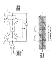
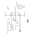
- an exemplary Class D amplifier 10 is shown to include a sawtooth waveform generator 14.
- a sawtooth signal V saw includes a positive sloped portion that increases from a minimum value to a maximum value followed by a return to the minimum value with an almost-infinite negative slope.
- the sawtooth signal V saw is input to an inverting input of a comparator 18.
- An input signal V IN such as an audio signal is input to a non-inverting input of the comparator 18.
- An output of the comparator 18 is input to first and second transistors 20 and 22 that are operated as switches.
- the first transistor 20 is a PMOS transistor and the second transistor 22 is an NMOS transistor.
- the output of the comparator 18 is also inverted by an inverter 24 and input to third and fourth transistors 26 and 28 that are also operated as switches.
- the third transistor 26 is a PMOS transistor and the fourth transistor 28 is an NMOS transistor.
- the sawtooth signal V saw is compared to the input signal V IN .
- the output is high.
- the input signal V IN is less than the sawtooth signal V saw
- the output is low.
- the input signal V IN is greater than the sawtooth signal V saw
- the output is high.
- the transistors 20, 22, 26 and 28 are switched on and off to drive current through a load 40 as depicted in FIG. 1.
- class-D amplifiers are known from US4415862 and the article “Parallel Phase Shifted Carrier Pulse Width Modulation (PSCPWM)-A novel approach to switching power amplifier design", by Karsten Nielsen, Bang & Olufsen, Denmark, XP001055906.
- PSCPWM Parallel Phase Shifted Carrier Pulse Width Modulation
- a Class D amplifier that receives an input signal comprises a ramp generator that generates a ramp signal and an inverted ramp signal.
- a signal generator generates a first signal when the ramp signal transitions from less than the input signal to greater than the input signal and when the inverted ramp signal transitions from less than the input signal to greater than the input signal.
- the signal generator generates a second signal when the ramp signal transitions from greater than the input signal to less than the input signal and when the inverted ramp signal transitions from greater than the input signal to less than the input signal.
- the signal generator comprises an edge detector.
- the signal generator further comprises a phase detector.
- the edge detector comprises a first comparator that compares the ramp signal to the input signal and a second comparator that compares the inverted ramp signal to the input signal.
- the edge detector generates a first pulse when rising edges occur in outputs of the first and second comparators and generates a second pulse when falling edges occur in the outputs of the first and second comparators.
- the edge detector comprises a first one shot that receives an output of the first comparator and that generates the first pulse when a rising edge occurs.
- a second one shot receives an output of the first comparator and generates the second pulse when a falling edge occurs.
- a third one shot receives an output of the second comparator and generates the first pulse when a rising edge occurs.
- a fourth one shot receives an output of the second comparator and generates the second pulse when a falling edge occurs.
- a frequency of the ramp signal is approximately two orders of magnitude higher than a frequency of the input signal.
- a positive slope of the ramp signal is approximately equal to a negative slope of the ramp signal and wherein a positive slope of the inverted ramp signal is approximately equal to a negative slope of the inverted ramp signal.
- An output stage receives the first and second signals from the signal generator and selectively drives output current based on the first and second signals.
- the output stage includes a single ended drive stage or a balanced H-bridge.
- a system comprises the Class D amplifier and further comprises a load that receives the output current.
- the load comprises an audio speaker.
- the Class D amplifier further comprises a low pass filter that is arranged between the output stage and the load.
- a method for operating a Class D amplifier that receives an input signal comprises generating a ramp signal and an inverted ramp signal.
- a first signal is generated when the ramp signal transitions from less than the input signal to greater than the input signal.
- the first signal is generated when the inverted ramp signal transitions from less than the input signal to greater than the input signal.
- a second signal is generated when the ramp signal transitions from greater than the input signal to less than the input signal.
- the second signal is generated when the inverted ramp signal transitions from greater than the input signal to less than the input signal.
- An output current is selectively driven based on the first and second signals.
- a frequency of the ramp signal is approximately two orders of magnitude higher than a frequency of the input signal and wherein a positive slope of the ramp signal is approximately equal to a negative slope of the ramp signal.
- the output current is low pass filtered.
- FIG. 1 is an electrical schematic of a Class D amplifier according to the prior art
- FIG. 2 is a waveform diagram illustrating a sawtooth signal V saw and an input signal V IN according to the prior art
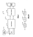
- FIG. 3 is a functional block diagram of a Class D amplifier according to the present invention.
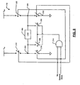
- FIG. 4 is electrical schematic of one exemplary implementation of the Class D amplifier of FIG. 3;
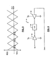
- FIG. 5 is a waveform diagram of a ramp signal V RAMP and an input signal V IN according to the present invention
- FIG. 6 illustrates an exemplary output stage of the Class D amplifier according to the present invention
- FIG. 7 illustrates a single ended output stage for the Class D amplifier according to the present invention
- FIG. 8 illustrates a balanced H-bridge output stage for the Class D amplifier according to the present invention
- FIG. 9 illustrates an alternate balanced H-bridge output stage for the Class D amplifier according to the present invention.
- FIG. 10 illustrates low pass filters of the Class D amplifier and the load.
- the Class D amplifier 100 includes a ramp generator 110 that generates a ramp signal (V RAMP ) and an inverted ramp signal ( V RAMP ⁇ ) .
- V RAMP a ramp signal
- V RAMP ⁇ an inverted ramp signal
- the terms ramp signal and inverted ramp signal refer to signals having alternating positive and negative slopes, which are substantially equal.
- the ramp signal V RAMP is output to a signal generator 111 that generates UP and DOWN signals for an output stage 118.
- the output stage 118 drives current through the load based on the UP and DOWN signals.
- the signal generator 111 includes an edge detector 114 and a phase detector 116.
- the ramp signal V RAMP , the inverted ramp signal V RAMP ⁇ and the input signal V IN are output to the edge detector circuit 114.
- the edge detector circuit 114 outputs first and second pulses when rising and falling edges of the ramp and inverted ramp signals transition above and below, respectively, the input signal. In other words, the edge detector circuit 114 outputs a first pulse when V RAMP transitions from a value less than V IN to a value greater than V IN and a second pulse when V RAMP transitions from a value greater than V IN to a value less than V IN , respectively. The edge detector circuit 114 also outputs the first pulse when V RAMP ⁇ transitions from a value less than V IN to a value greater than V IN and the second pulse when V RAMP ⁇ transitions from a value greater than V IN to a value less than V IN , respectively.
- Outputs of the edge detector circuit 114 are input to a phase detector 116.
- the phase detector 116 sends an UP signal when the first pulse is received until the second pulse is received.
- the phase detector 116 sends a DOWN signal until the first pulse is received.
- An output of the phase detector 116 is transmitted to an output stage 118, which drives current across the load based on the UP and DOWN signals.
- the edge detector circuit 114 includes comparators 119-1 and 119-2 and one-shot circuits 120-1 and 120-3 and 120-2 and 120-4, respectively.
- the ramp signal V RAMP is output to a non-inverting input of the first comparator 119-1.
- the inverted ramp signal V RAMP ⁇ is output to a non-inverting input of the second comparator 119-2.
- the input signal V IN is input to inverting inputs of the comparators 119-1 and 119-2.
- Outputs of the comparators 119-1 and 119-2 are input to the one-shot circuits 120.
- the one-shot circuits 120-1 and 120-2 generate an output pulse when there is a positive edge sensed at the input thereof.
- the one-shot circuits 120-3 and 120-4 generate an output pulse when there is a negative edge sensed at the input thereof.
- Outputs of the one-shot circuits 120-1 and 120-2 are input to OR gate 130.
- Outputs of the one-shot circuits 120-3 and 120-4 are input to OR gate 132.
- Outputs of the OR gates 130 and 132 are input to a phase detector 116.
- the phase detector 116 operates in a manner that is similar to phase detectors in modern phase locked loops (PLLs). When there is no phase error in modern PLLs, a very small up and down pulse current is generated. In a Class D amplifier, however, voltage pulses are used instead of current.
- the phase detector 116 includes a flip-flop 142 that communicates with the output of the OR gate 130 and a flip-flop 144 that communicates with the output of the OR gate 132.
- D inputs of the flip-flops 142 and 144 are connected to a voltage bias V BB .
- a Q output of the flip-flop 142 provides a first or UP signal.
- a Q output of the flip-flop 144 provides a second or DOWN signal.
- the UP signal and the DOWN signal are fed back through an AND gate 150 and a delay 152 to reset (R) inputs of the flip-flops 142 and 144.
- the UP signal and the DOWN signal are also transmitted to an output stage 118, as will be described below.
- the ramp signal preferably has a frequency that is 2 orders of magnitude higher than the input frequency (e.g. 20kHz and 1-2 MHz).
- the ramp signal V RAMP the inverted ramp signal V RAMP ⁇
- an input signal V IN is shown.
- the UP signal is initiated on a rising edge of either the ramp signal V RAMP or the inverted ramp signal V RAMP ⁇ crossing the input signal V IN .
- the DOWN signal is initiated on a falling edge of either the ramp signal V RAMP or the inverted ramp signal V RAMP ⁇ . crossing the input signal V IN .
- an exemplary output stage 118 includes an amplifier 180 that is switched on when the UP signal has a first state and off when the UP signal has a second state.
- the amplifier 182 is switched on when the DOWN signal has a first state and off when the UP signal has a second state.
- an alternate output stage 118 is configured as a single ended drive stage.
- the output stage 118 includes an AND gate 190 with inverted inputs, which are connected to the UP signal and a delayed DOWN signal.
- the UP signal controls a first switch 194.
- An output of the AND gate 190 controls a second switch 196.
- the first switch 194 selectively connects V DD to a node 200.
- the second switch 196 selectively connects the node 200 to ground.
- the delayed DOWN signal controls a third switch 198, which selectively connects the node 200 to negative V EE .
- the load 184 is connected between the node 200 and ground.
- the DOWN signal is delayed by at least the minimum pulse width of the phase detector 116 to avoid conflict between the switches 194 and 198.
- the delay is preferably at least two times the minimum delay described above.
- the switch 196 is on only when the UP and the delayed DOWN signals are inactive. In PLL applications, the DOWN signal does not need to be delayed because current is used. Therefore UP and DOWN signals can occur at the same time. With voltage signals, the DOWN signal is preferably delayed to avoid the crowbar short-circuit effect of both the top and bottom transistors being on.
- an alternate output stage 118 is configured as a balanced H-bridge implementation.
- the UP signal controls first and second switches 210 and 212 and is input to an AND gate 214 with inverted inputs.
- the delayed DOWN signal controls switches 218 and 222 and is input to AND gate 214, which has inverted inputs.
- the output of the AND gates 214 controls switches 230 and 232, which are connected across the load 184.
- the switches 210 and 222 are connected between V DD and nodes 234 and 236, respectively.
- the switches 218 and 212 are connected between the nodes 234 and 236, respectively, and ground.
- FIG. 9 an alternate output stage 118 that is similar to the output stage in FIG. 8 is shown.
- the output stage 118 in FIG. 9 includes an additional switch 250 that is controlled by the output of the AND gate 214.
- the switch 250 is connected across the load 184.
- the output common mode of the output stages 118 that are shown in FIGs. 8 and 9 does not move around and is centered between the positive and negative power supplies.
- the signal to the load 184 can be filtered using one or more low pass filter circuits 300.
- the low pass filter circuits 300 may include one or more inductors and/or capacitors that remove high frequency switching components.
- the filter may include a series inductor and a parallel capacitor.
- the optional filters 300 may not be needed if the load is an inductive load such as a loudspeaker load, which is mechanically similar to a low pass filter.
Landscapes
- Engineering & Computer Science (AREA)
- Power Engineering (AREA)
- Amplifiers (AREA)
Claims (20)
- Klasse-D-Verstärker (100), der ein Eingangssignal empfängt, umfassend:einen Sägezahngenerator (110), der ein Sägezahnsignal und ein invertiertes Sägezahnsignal erzeugt; undeinen Signalgenerator (111), der, nach einem Übergang des besagten Sägezahnsignals von einem Wert, der geringer als das Eingangssignal ist, zu einem Wert, der größer als das Eingangssignal ist, und nach einem Übergang des besagten invertierten Sägezahnsignals von einem Wert, der geringer als das Eingangssignal ist, zu einem Wert, der größer als das Eingangssignal ist, einen ersten Zustand eines ersten Signals erzeugt,wobei besagter Signalgenerator (111) nach einem Übergang des besagten Sägezahnsignals von einem Wert, der größer als das Eingangssignal ist, zu einem Wert, der kleiner als das Eingangssignal ist, und nach einem Übergang des besagten invertierten Sägezahnsignals von einem Wert, der größer als das Eingangssignal ist, zu einem Wert, der kleiner als das Eingangssignal ist, einen ersten Zustand eines zweiten Signals erzeugt.
- Klasse-D-Verstärker (100) nach Anspruch 1, wobei, sobald besagter Signalgenerator (111) den besagten ersten Zustand von einem des besagten ersten und des besagten zweiten Signals ausgibt, der besagte Signalgenerator (111) zu dem besagten ersten Zustand des anderen des besagten ersten und des besagten zweiten Signals selektiv übergeht, wenn der besagte erste Zustand des anderen des besagten ersten und des besagten zweiten Signals erzeugt wird.
- Klasse-D-Verstärker (100) nach Anspruch 1, wobei besagter Signalgenerator (111) einen Kantendetektor (114) umfasst.
- Klasse-D-Verstärker (100) nach Anspruch 3, wobei besagter Signalgenerator (111) weiter einen Phasendetektor (116) umfasst.
- Klasse-D-Verstärker (100) nach Anspruch 3, wobei besagter Kantendetektor (114) umfasst:einen ersten Komparator (119-1), der das besagte Sägezahnsignal mit dem Eingangssignal vergleicht; undeinen zweiten Komparator (119-2), der besagtes invertiertes Sägezahnsignal mit dem Eingangssignal vergleicht.
- Klasse-D-Verstärker (100) nach Anspruch 5, wobei der besagte Kantendetektor (114) einen ersten Puls erzeugt, wenn steigende Flanken in den Ausgängen des besagten ersten und des besagten zweiten Komparators (119-1, 119-2) auftreten, und einen zweiten Puls erzeugt, wenn fallende Flanken in den besagten Ausgängen des besagten ersten und des besagten zweiten Komparators (119-1, 119-2) auftreten.
- Klasse-D-Verstärker (100) nach Anspruch 6, wobei besagter Kantendetektor (114) umfasst:einen ersten One-Shot (120-1), der einen Ausgang des besagten ersten Komparators (119-1) empfängt und der besagten ersten Puls erzeugt, wenn eine steigende Flanke auftritt;einen zweiten One-Shot (120-2), der einen Ausgang des besagten ersten Komparators (119-1) empfängt und der besagten zweiten Puls erzeugt, wenn eine fallende Flanke auftritt;einen dritten One-Shot (120-3), der einen Ausgang des besagten zweiten Komparators (119-2) empfängt und der besagten ersten Puls erzeugt, wenn eine steigende Flanke auftritt; undeinen vierten One-Shot (120-4), der einen Ausgang des besagten zweiten Komparators (119-2) empfängt und der besagten zweiten Puls erzeugt, wenn eine fallende Flanke auftritt.
- Klasse-D-Verstärker (100) nach Anspruch 1, wobei eine Frequenz des besagten Sägezahnsignals näherungsweise zwei Größenordnungen höher ist als eine Frequenz des Eingangssignals.
- Klasse-D-Verstärker (100) nach Anspruch 1, wobei eine positive Steigung des besagten Sägezahnsignals annähernd gleichgroß ist wie eine negative Steigung des besagten Sägezahnsignals und wobei eine positive Steigung des besagten invertierten Sägezahnsignals annähernd gleichgroß ist wie eine negative Steigung des besagten invertierten Sägezahnsignals.
- Klasse-D-Verstärker (100) nach Anspruch 1, weiter umfassend eine Ausgangsstufe (118), die das besagte erste und das besagte zweite Signal von besagtem Signalgenerator (111) empfängt und die, beruhend auf dem besagten ersten und dem besagten zweiten Signal, einen Ausgangsstrom selektiv treibt.
- Klasse-D-Verstärker (100) nach Anspruch 10, wobei besagte Ausgangsstufe (118) Schalter beinhaltet, die durch das besagte erste und das besagte zweite Signal gesteuert werden.
- Klasse-D-Verstärker (100) nach Anspruch 10, wobei besagte Ausgangsstufe (118) eine abgeglichene H-Brücke beinhaltet.
- System, das den Klasse-D-Verstärker (100) nach Anspruch 10 umfasst und weiter eine Last umfasst, die den besagten Ausgangsstrom empfängt.
- System nach Anspruch 13, wobei besagte Last einen Lautsprecher umfasst.
- System nach Anspruch 13, wobei besagter Klasse-D-Verstärker (100) weiter einen Tiefpassfilter umfasst, der zwischen besagter Ausgangsstufe (118) und besagter Last angeordnet ist.
- Verfahren zum Betreiben eines Klasse-D-Verstärkers, der ein Eingangssignal empfängt, umfassend:Erzeugen eines Sägezahnsignals;Erzeugen eines invertierten Sägezahnsignals;Erzeugen, nach einem Übergang des besagten Sägezahnsignals von einem Wert, der geringer als das Eingangssignal ist, zu einem Wert, der größer als das Eingangssignal ist, und nach einem Übergang des besagten invertierten Sägezahnsignals von einem Wert, der geringer als das Eingangssignal ist, zu einem Wert, der größer als das Eingangssignal ist, eines ersten Zustandes eines ersten Signals;Erzeugen, nach einem Übergang des besagten Sägezahnsignals von einem Wert, der größer als das Eingangssignal ist, zu einem Wert, der kleiner als das Eingangssignal ist, und nach einem Übergang des besagten invertierten Sägezahnsignals von einem Wert, der größer als das Eingangssignal ist, zu einem Wert, der kleiner als das Eingangssignal ist, eines ersten Zustandes eines zweiten Signals.
- Verfahren nach Anspruch 16, das, wenn besagter erster Zustand von einem des besagten ersten und des besagten zweiten Signals ausgegeben wird, weiter ein selektives Übergehen zu besagtem ersten Zustand des anderen des besagten ersten und des besagten zweiten Signals umfasst, wenn besagter erster Zustand des anderen des besagten ersten Signals und des besagten zweiten Signals erzeugt wird.
- Verfahren nach Anspruch 16, weiter umfassend ein selektives Treiben eines Ausgangsstroms beruhend auf besagtem ersten und besagtem zweiten Signal.
- Verfahren nach Anspruch 16, wobei eine Frequenz des besagten Sägezahnsignals annähernd zwei Größenordnungen höher ist als eine Frequenz des Eingangssignals und wobei eine positive Steigung des besagten Sägezahnsignals annähernd gleichgroß ist wie eine negative Steigung des besagten Sägezahnsignals.
- Verfahren nach Anspruch 18, das weiter ein Tiefpassfiltem des besagten Ausgangsstroms umfasst.
Applications Claiming Priority (2)
| Application Number | Priority Date | Filing Date | Title |
|---|---|---|---|
| US10/703,135 US7190224B2 (en) | 2003-11-06 | 2003-11-06 | Class D amplifier |
| US703135 | 2003-11-06 |
Publications (2)
| Publication Number | Publication Date |
|---|---|
| EP1530286A1 EP1530286A1 (de) | 2005-05-11 |
| EP1530286B1 true EP1530286B1 (de) | 2007-01-10 |
Family
ID=34435561
Family Applications (1)
| Application Number | Title | Priority Date | Filing Date |
|---|---|---|---|
| EP04011557A Expired - Lifetime EP1530286B1 (de) | 2003-11-06 | 2004-05-14 | Klasse-D Verstärker |
Country Status (6)
| Country | Link |
|---|---|
| US (5) | US7190224B2 (de) |
| EP (1) | EP1530286B1 (de) |
| JP (1) | JP4015648B2 (de) |
| CN (1) | CN100508372C (de) |
| DE (1) | DE602004004230T2 (de) |
| TW (1) | TWI337805B (de) |
Families Citing this family (21)
| Publication number | Priority date | Publication date | Assignee | Title |
|---|---|---|---|---|
| US7190224B2 (en) * | 2003-11-06 | 2007-03-13 | Marvell World Trade Ltd. | Class D amplifier |
| JP2006211523A (ja) * | 2005-01-31 | 2006-08-10 | Asahi Kasei Microsystems Kk | デジタルスイッチング回路 |
| AU2006345024C1 (en) | 2005-07-28 | 2012-07-26 | Nanocomp Technologies, Inc. | Systems and methods for formation and harvesting of nanofibrous materials |
| US7279973B1 (en) * | 2005-09-23 | 2007-10-09 | Ami Semiconductor Belgium Bvba | H-bridge utilizing intermediate switching phase(s) |
| JP4585970B2 (ja) * | 2006-01-05 | 2010-11-24 | Okiセミコンダクタ株式会社 | パルス幅変調装置 |
| US8284963B2 (en) * | 2007-09-11 | 2012-10-09 | Texas Instruments Incorporated | Method and apparatus for diminishing mismatch effects between switched signals |
| US7701307B2 (en) * | 2008-04-01 | 2010-04-20 | Silicon Laboratories, Inc. | System and method of changing a PWM power spectrum |
| US7791521B2 (en) * | 2008-04-01 | 2010-09-07 | Silicon Laboratories, Inc. | System and method of changing a PWM power spectrum |
| US7598895B1 (en) * | 2008-04-01 | 2009-10-06 | Silicon Laboratories, Inc. | System and method of altering a PWM carrier power spectrum |
| GB2459304B (en) | 2008-04-18 | 2013-02-20 | Nujira Ltd | Improved pulse width modulation |
| US8995691B2 (en) | 2008-07-14 | 2015-03-31 | Audera Acoustics Inc. | Audio amplifier |
| US7746123B2 (en) * | 2008-09-09 | 2010-06-29 | Texas Instruments Incorporated | Switching system with reduced EMI |
| US8269475B2 (en) * | 2009-02-17 | 2012-09-18 | Texas Instruments Incorporated | Class DH amplifier |
| US8130128B2 (en) | 2010-03-30 | 2012-03-06 | Silicon Laboratores Inc. | System and method for generating shaped noise |
| TWI429192B (zh) * | 2010-06-14 | 2014-03-01 | Upi Semiconductor Corp | 功率放大器及具有功率放大器的處理裝置 |
| CA2828263C (en) * | 2011-02-28 | 2015-05-19 | Widex A/S | Hearing aid with an h-bridge output stage and a method of driving an output stage |
| DE102011115503A1 (de) * | 2011-10-11 | 2013-04-11 | Astrium Gmbh | Messung des Ausgangstroms einer Verstärkerschaltung |
| CN102545855B (zh) * | 2012-01-17 | 2017-04-05 | 南京航空航天大学 | 基于闭环控制的功率开关管驱动方法及系统 |
| DE102015212232B4 (de) * | 2015-06-30 | 2020-03-05 | TRUMPF Hüttinger GmbH + Co. KG | Leistungscombiner zur Kopplung von Hochfrequenzsignalen und Leistungscombineranordnung mit einem solchen Leistungscombiner |
| US10033366B2 (en) * | 2016-12-22 | 2018-07-24 | Silanna Asia Pte Ltd | Minimum pulse-width assurance |
| WO2018211698A1 (ja) * | 2017-05-19 | 2018-11-22 | ヤマハ株式会社 | 音響処理装置および音響処理装置の制御方法 |
Family Cites Families (28)
| Publication number | Priority date | Publication date | Assignee | Title |
|---|---|---|---|---|
| JPS56136008A (en) | 1980-03-28 | 1981-10-23 | Pioneer Electronic Corp | Pulse-width modulating and amplifying circuit |
| US4404511A (en) * | 1980-10-23 | 1983-09-13 | The United States Of America As Represented By The Administrator Of The National Aeronautics And Space Administration | Motor power factor controller with a reduced voltage starter |
| US4584566A (en) * | 1984-12-21 | 1986-04-22 | Honeywell Inc. | Analog to digital converter |
| US4791341A (en) * | 1988-01-19 | 1988-12-13 | General Electric Company | Speed reducing control system for a polyphase electric motor |
| GB2247793A (en) * | 1990-09-06 | 1992-03-11 | Motorola Inc | Control of pulse power amplifier rise and fall |
| US5077539A (en) | 1990-12-26 | 1991-12-31 | Apogee Technology, Inc. | Switching amplifier |
| US5204809A (en) | 1992-04-03 | 1993-04-20 | International Business Machines Corporation | H-driver DC-to-DC converter utilizing mutual inductance |
| US5479134A (en) * | 1993-09-20 | 1995-12-26 | Rohm Co., Ltd. | Power amplifier circuit for audio signal and audio device using the same |
| US5479337A (en) * | 1993-11-30 | 1995-12-26 | Kaiser Aerospace And Electronics Corporation | Very low power loss amplifier for analog signals utilizing constant-frequency zero-voltage-switching multi-resonant converter |
| US5841313A (en) * | 1995-08-30 | 1998-11-24 | Cherry Semiconductor Corporation | Switch with programmable delay |
| US5617058A (en) | 1995-11-13 | 1997-04-01 | Apogee Technology, Inc. | Digital signal processing for linearization of small input signals to a tri-state power switch |
| US6049473A (en) * | 1999-02-11 | 2000-04-11 | Delta Electronics, Inc. | Harmonic-injection control technique for three-phase, discontinuous-conduction-mode, high-power-factor boost rectifiers with improved line-transient response |
| DE69919500T2 (de) * | 1999-02-11 | 2005-09-08 | Stmicroelectronics S.R.L., Agrate Brianza | PWM Leistungsverstärker mit digitalem Eingang |
| US6430220B1 (en) * | 2000-09-19 | 2002-08-06 | Apogee Technology Inc. | Distortion reduction method and apparatus for linearization of digital pulse width modulation by efficient calculation |
| US6348781B1 (en) * | 2000-12-11 | 2002-02-19 | Motorola, Inc. | Buck or boost power converter |
| US6362986B1 (en) | 2001-03-22 | 2002-03-26 | Volterra, Inc. | Voltage converter with coupled inductive windings, and associated methods |
| US7200187B2 (en) * | 2001-07-26 | 2007-04-03 | O'brien Thomas J | Modulator for digital amplifier |
| FR2829653A1 (fr) * | 2001-09-07 | 2003-03-14 | St Microelectronics Sa | Dispositif d'alimentation a decoupage adapte pour les faibles consommations de courant, et telephone cellulaire dote d'un tel dispositif |
| US6552607B1 (en) | 2001-11-12 | 2003-04-22 | Apogee Technology Inc. | Time division multiplexed PWM amplifier |
| KR100435182B1 (ko) * | 2002-02-05 | 2004-06-09 | 주식회사 디지털앤아날로그 | Pwm 부궤환에 의한 디지털 pwm 입력 d급 음향 증폭기 |
| CA2414965A1 (en) * | 2002-12-23 | 2004-06-23 | Alan Bayko | Amplifier |
| US7002406B2 (en) * | 2003-05-16 | 2006-02-21 | Texas Instruments Incorporated | Loop filter for class D amplifiers |
| US6847257B2 (en) * | 2003-05-23 | 2005-01-25 | Maxim Integrated Products, Inc. | Efficient minimum pulse spread spectrum modulation for filterless class D amplifiers |
| US7378904B2 (en) * | 2003-10-15 | 2008-05-27 | Texas Instruments Incorporated | Soft transitions between muted and unmuted states in class D audio amplifiers |
| US7298209B1 (en) | 2003-11-06 | 2007-11-20 | Marvell World Trade Ltd. | Class D amplifier |
| US7190224B2 (en) | 2003-11-06 | 2007-03-13 | Marvell World Trade Ltd. | Class D amplifier |
| KR100588334B1 (ko) * | 2005-03-29 | 2006-06-09 | 삼성전자주식회사 | 슈도 슈미트 트리거 회로를 이용한 디시-디시 컨버터 및펄스 폭 변조방법 |
| US7262658B2 (en) * | 2005-07-29 | 2007-08-28 | Texas Instruments Incorporated | Class-D amplifier system |
-
2003
- 2003-11-06 US US10/703,135 patent/US7190224B2/en not_active Expired - Lifetime
-
2004
- 2004-05-14 DE DE602004004230T patent/DE602004004230T2/de not_active Expired - Lifetime
- 2004-05-14 EP EP04011557A patent/EP1530286B1/de not_active Expired - Lifetime
- 2004-06-24 TW TW093118269A patent/TWI337805B/zh not_active IP Right Cessation
- 2004-08-03 CN CNB2004100704773A patent/CN100508372C/zh not_active Expired - Lifetime
- 2004-08-06 JP JP2004231068A patent/JP4015648B2/ja not_active Expired - Lifetime
-
2005
- 2005-06-28 US US11/170,440 patent/US7242248B1/en not_active Expired - Lifetime
-
2007
- 2007-11-16 US US11/985,653 patent/US7468631B1/en not_active Expired - Lifetime
-
2008
- 2008-12-23 US US12/342,768 patent/US7646240B2/en not_active Expired - Fee Related
-
2010
- 2010-01-12 US US12/685,884 patent/US7884670B2/en not_active Expired - Lifetime
Also Published As
| Publication number | Publication date |
|---|---|
| CN1614882A (zh) | 2005-05-11 |
| TWI337805B (en) | 2011-02-21 |
| US7646240B2 (en) | 2010-01-12 |
| DE602004004230T2 (de) | 2007-11-15 |
| US20050099231A1 (en) | 2005-05-12 |
| US20100111331A1 (en) | 2010-05-06 |
| TW200516842A (en) | 2005-05-16 |
| US20090102556A1 (en) | 2009-04-23 |
| US7190224B2 (en) | 2007-03-13 |
| EP1530286A1 (de) | 2005-05-11 |
| JP4015648B2 (ja) | 2007-11-28 |
| DE602004004230D1 (de) | 2007-02-22 |
| US7242248B1 (en) | 2007-07-10 |
| JP2005143077A (ja) | 2005-06-02 |
| CN100508372C (zh) | 2009-07-01 |
| US7884670B2 (en) | 2011-02-08 |
| US7468631B1 (en) | 2008-12-23 |
Similar Documents
| Publication | Publication Date | Title |
|---|---|---|
| EP1530286B1 (de) | Klasse-D Verstärker | |
| US7298209B1 (en) | Class D amplifier | |
| US7142050B2 (en) | Recovery from clipping events in a class D amplifier | |
| US7332962B2 (en) | Filterless class D power amplifier | |
| US7728666B2 (en) | Close-loop class-D audio amplifier and control method thereof | |
| US20070109049A1 (en) | Filterless class d power amplifier | |
| JP2003115730A (ja) | Pwm変調回路及び電力増幅回路 | |
| US7855597B2 (en) | Class-D amplifier | |
| KR101067985B1 (ko) | D급 증폭기 회로 | |
| EP3665774B1 (de) | Fehlerverstärker | |
| US10749486B2 (en) | Class D amplifier current feedback | |
| EP1184973A1 (de) | Leistungsverstärkervorrichtung | |
| US20060145755A1 (en) | Square wave modulation design for a class-D audio amplifier | |
| US11159132B2 (en) | Class D amplifier stereo to mono converter | |
| US7768347B2 (en) | Device comprising a switching amplifier and a load | |
| US7279966B2 (en) | Systems for pseudo-BD modulation | |
| JP2007209038A (ja) | 電力増幅回路 | |
| US20210367566A1 (en) | Audio amplifier having idle mode | |
| KR20020034677A (ko) | 고효율 스위칭 증폭기 | |
| Bryson | Benefits of class-G and class-H boost in audio amplifiers | |
| JP2006093764A (ja) | ディジタルパワーアンプ | |
| KR101349002B1 (ko) | 증폭 회로 및 증폭 방법 | |
| CN113691223A (zh) | 具有空闲模式的音频放大器 |
Legal Events
| Date | Code | Title | Description |
|---|---|---|---|
| PUAI | Public reference made under article 153(3) epc to a published international application that has entered the european phase |
Free format text: ORIGINAL CODE: 0009012 |
|
| AK | Designated contracting states |
Kind code of ref document: A1 Designated state(s): AT BE BG CH CY CZ DE DK EE ES FI FR GB GR HU IE IT LI LU MC NL PL PT RO SE SI SK TR |
|
| AX | Request for extension of the european patent |
Extension state: AL HR LT LV MK |
|
| 17P | Request for examination filed |
Effective date: 20051111 |
|
| AKX | Designation fees paid |
Designated state(s): DE FR GB |
|
| GRAP | Despatch of communication of intention to grant a patent |
Free format text: ORIGINAL CODE: EPIDOSNIGR1 |
|
| GRAS | Grant fee paid |
Free format text: ORIGINAL CODE: EPIDOSNIGR3 |
|
| GRAA | (expected) grant |
Free format text: ORIGINAL CODE: 0009210 |
|
| AK | Designated contracting states |
Kind code of ref document: B1 Designated state(s): DE FR GB |
|
| REG | Reference to a national code |
Ref country code: GB Ref legal event code: FG4D |
|
| REF | Corresponds to: |
Ref document number: 602004004230 Country of ref document: DE Date of ref document: 20070222 Kind code of ref document: P |
|
| ET | Fr: translation filed | ||
| PLBE | No opposition filed within time limit |
Free format text: ORIGINAL CODE: 0009261 |
|
| STAA | Information on the status of an ep patent application or granted ep patent |
Free format text: STATUS: NO OPPOSITION FILED WITHIN TIME LIMIT |
|
| 26N | No opposition filed |
Effective date: 20071011 |
|
| REG | Reference to a national code |
Ref country code: FR Ref legal event code: PLFP Year of fee payment: 13 |
|
| REG | Reference to a national code |
Ref country code: FR Ref legal event code: PLFP Year of fee payment: 14 |
|
| REG | Reference to a national code |
Ref country code: FR Ref legal event code: PLFP Year of fee payment: 15 |
|
| REG | Reference to a national code |
Ref country code: DE Ref legal event code: R082 Ref document number: 602004004230 Country of ref document: DE Representative=s name: GRUENECKER PATENT- UND RECHTSANWAELTE PARTG MB, DE Ref country code: DE Ref legal event code: R081 Ref document number: 602004004230 Country of ref document: DE Owner name: MARVELL ASIA PTE, LTD., SG Free format text: FORMER OWNER: MARVELL WORLD TRADE LTD., ST. MICHAEL, BB |
|
| REG | Reference to a national code |
Ref country code: GB Ref legal event code: 732E Free format text: REGISTERED BETWEEN 20210805 AND 20210811 |
|
| PGFP | Annual fee paid to national office [announced via postgrant information from national office to epo] |
Ref country code: FR Payment date: 20220526 Year of fee payment: 19 |
|
| P01 | Opt-out of the competence of the unified patent court (upc) registered |
Effective date: 20230508 |
|
| PGFP | Annual fee paid to national office [announced via postgrant information from national office to epo] |
Ref country code: DE Payment date: 20230530 Year of fee payment: 20 |
|
| PGFP | Annual fee paid to national office [announced via postgrant information from national office to epo] |
Ref country code: GB Payment date: 20230523 Year of fee payment: 20 |
|
| REG | Reference to a national code |
Ref country code: DE Ref legal event code: R071 Ref document number: 602004004230 Country of ref document: DE |
|
| PG25 | Lapsed in a contracting state [announced via postgrant information from national office to epo] |
Ref country code: FR Free format text: LAPSE BECAUSE OF NON-PAYMENT OF DUE FEES Effective date: 20230531 |
|
| REG | Reference to a national code |
Ref country code: GB Ref legal event code: PE20 Expiry date: 20240513 |
|
| PG25 | Lapsed in a contracting state [announced via postgrant information from national office to epo] |
Ref country code: GB Free format text: LAPSE BECAUSE OF EXPIRATION OF PROTECTION Effective date: 20240513 |
|
| PG25 | Lapsed in a contracting state [announced via postgrant information from national office to epo] |
Ref country code: GB Free format text: LAPSE BECAUSE OF EXPIRATION OF PROTECTION Effective date: 20240513 |