EP1529276B1 - Elektrolumineszenzanzeigebauelement mit pixeln mit nmos-transistoren - Google Patents
Elektrolumineszenzanzeigebauelement mit pixeln mit nmos-transistoren Download PDFInfo
- Publication number
- EP1529276B1 EP1529276B1 EP03784336A EP03784336A EP1529276B1 EP 1529276 B1 EP1529276 B1 EP 1529276B1 EP 03784336 A EP03784336 A EP 03784336A EP 03784336 A EP03784336 A EP 03784336A EP 1529276 B1 EP1529276 B1 EP 1529276B1
- Authority
- EP
- European Patent Office
- Prior art keywords
- display element
- transistor
- voltage
- pixels
- gate
- Prior art date
- Legal status (The legal status is an assumption and is not a legal conclusion. Google has not performed a legal analysis and makes no representation as to the accuracy of the status listed.)
- Expired - Lifetime
Links
- 239000003990 capacitor Substances 0.000 claims abstract description 26
- 229910021417 amorphous silicon Inorganic materials 0.000 claims abstract description 25
- 229910021424 microcrystalline silicon Inorganic materials 0.000 claims abstract description 20
- 239000011159 matrix material Substances 0.000 claims abstract description 16
- 239000004020 conductor Substances 0.000 claims description 21
- 238000000034 method Methods 0.000 claims description 13
- XUIMIQQOPSSXEZ-UHFFFAOYSA-N Silicon Chemical compound [Si] XUIMIQQOPSSXEZ-UHFFFAOYSA-N 0.000 claims description 3
- 229910052710 silicon Inorganic materials 0.000 claims description 3
- 239000010703 silicon Substances 0.000 claims description 3
- 230000008878 coupling Effects 0.000 claims 1
- 238000010168 coupling process Methods 0.000 claims 1
- 238000005859 coupling reaction Methods 0.000 claims 1
- 239000000463 material Substances 0.000 description 8
- 239000004973 liquid crystal related substance Substances 0.000 description 5
- 239000002861 polymer material Substances 0.000 description 4
- 239000000758 substrate Substances 0.000 description 4
- 239000010409 thin film Substances 0.000 description 4
- 229920000547 conjugated polymer Polymers 0.000 description 3
- 238000005516 engineering process Methods 0.000 description 3
- 238000005334 plasma enhanced chemical vapour deposition Methods 0.000 description 3
- 238000000623 plasma-assisted chemical vapour deposition Methods 0.000 description 3
- 238000003491 array Methods 0.000 description 2
- 238000011161 development Methods 0.000 description 2
- 230000018109 developmental process Effects 0.000 description 2
- 229920000642 polymer Polymers 0.000 description 2
- 150000001875 compounds Chemical class 0.000 description 1
- 229910021419 crystalline silicon Inorganic materials 0.000 description 1
- 238000010586 diagram Methods 0.000 description 1
- 230000000694 effects Effects 0.000 description 1
- 239000011521 glass Substances 0.000 description 1
- 238000005286 illumination Methods 0.000 description 1
- 238000007641 inkjet printing Methods 0.000 description 1
- 239000002184 metal Substances 0.000 description 1
- 238000012986 modification Methods 0.000 description 1
- 230000004048 modification Effects 0.000 description 1
- 230000002093 peripheral effect Effects 0.000 description 1
- 239000004065 semiconductor Substances 0.000 description 1
- 238000004528 spin coating Methods 0.000 description 1
- 239000012780 transparent material Substances 0.000 description 1
Images
Classifications
-
- G—PHYSICS
- G09—EDUCATION; CRYPTOGRAPHY; DISPLAY; ADVERTISING; SEALS
- G09G—ARRANGEMENTS OR CIRCUITS FOR CONTROL OF INDICATING DEVICES USING STATIC MEANS TO PRESENT VARIABLE INFORMATION
- G09G3/00—Control arrangements or circuits, of interest only in connection with visual indicators other than cathode-ray tubes
- G09G3/20—Control arrangements or circuits, of interest only in connection with visual indicators other than cathode-ray tubes for presentation of an assembly of a number of characters, e.g. a page, by composing the assembly by combination of individual elements arranged in a matrix no fixed position being assigned to or needed to be assigned to the individual characters or partial characters
- G09G3/22—Control arrangements or circuits, of interest only in connection with visual indicators other than cathode-ray tubes for presentation of an assembly of a number of characters, e.g. a page, by composing the assembly by combination of individual elements arranged in a matrix no fixed position being assigned to or needed to be assigned to the individual characters or partial characters using controlled light sources
- G09G3/30—Control arrangements or circuits, of interest only in connection with visual indicators other than cathode-ray tubes for presentation of an assembly of a number of characters, e.g. a page, by composing the assembly by combination of individual elements arranged in a matrix no fixed position being assigned to or needed to be assigned to the individual characters or partial characters using controlled light sources using electroluminescent panels
- G09G3/32—Control arrangements or circuits, of interest only in connection with visual indicators other than cathode-ray tubes for presentation of an assembly of a number of characters, e.g. a page, by composing the assembly by combination of individual elements arranged in a matrix no fixed position being assigned to or needed to be assigned to the individual characters or partial characters using controlled light sources using electroluminescent panels semiconductive, e.g. using light-emitting diodes [LED]
- G09G3/3208—Control arrangements or circuits, of interest only in connection with visual indicators other than cathode-ray tubes for presentation of an assembly of a number of characters, e.g. a page, by composing the assembly by combination of individual elements arranged in a matrix no fixed position being assigned to or needed to be assigned to the individual characters or partial characters using controlled light sources using electroluminescent panels semiconductive, e.g. using light-emitting diodes [LED] organic, e.g. using organic light-emitting diodes [OLED]
- G09G3/3225—Control arrangements or circuits, of interest only in connection with visual indicators other than cathode-ray tubes for presentation of an assembly of a number of characters, e.g. a page, by composing the assembly by combination of individual elements arranged in a matrix no fixed position being assigned to or needed to be assigned to the individual characters or partial characters using controlled light sources using electroluminescent panels semiconductive, e.g. using light-emitting diodes [LED] organic, e.g. using organic light-emitting diodes [OLED] using an active matrix
- G09G3/3233—Control arrangements or circuits, of interest only in connection with visual indicators other than cathode-ray tubes for presentation of an assembly of a number of characters, e.g. a page, by composing the assembly by combination of individual elements arranged in a matrix no fixed position being assigned to or needed to be assigned to the individual characters or partial characters using controlled light sources using electroluminescent panels semiconductive, e.g. using light-emitting diodes [LED] organic, e.g. using organic light-emitting diodes [OLED] using an active matrix with pixel circuitry controlling the current through the light-emitting element
-
- G—PHYSICS
- G09—EDUCATION; CRYPTOGRAPHY; DISPLAY; ADVERTISING; SEALS
- G09G—ARRANGEMENTS OR CIRCUITS FOR CONTROL OF INDICATING DEVICES USING STATIC MEANS TO PRESENT VARIABLE INFORMATION
- G09G3/00—Control arrangements or circuits, of interest only in connection with visual indicators other than cathode-ray tubes
- G09G3/20—Control arrangements or circuits, of interest only in connection with visual indicators other than cathode-ray tubes for presentation of an assembly of a number of characters, e.g. a page, by composing the assembly by combination of individual elements arranged in a matrix no fixed position being assigned to or needed to be assigned to the individual characters or partial characters
- G09G3/22—Control arrangements or circuits, of interest only in connection with visual indicators other than cathode-ray tubes for presentation of an assembly of a number of characters, e.g. a page, by composing the assembly by combination of individual elements arranged in a matrix no fixed position being assigned to or needed to be assigned to the individual characters or partial characters using controlled light sources
- G09G3/30—Control arrangements or circuits, of interest only in connection with visual indicators other than cathode-ray tubes for presentation of an assembly of a number of characters, e.g. a page, by composing the assembly by combination of individual elements arranged in a matrix no fixed position being assigned to or needed to be assigned to the individual characters or partial characters using controlled light sources using electroluminescent panels
-
- G—PHYSICS
- G09—EDUCATION; CRYPTOGRAPHY; DISPLAY; ADVERTISING; SEALS
- G09G—ARRANGEMENTS OR CIRCUITS FOR CONTROL OF INDICATING DEVICES USING STATIC MEANS TO PRESENT VARIABLE INFORMATION
- G09G2300/00—Aspects of the constitution of display devices
- G09G2300/04—Structural and physical details of display devices
- G09G2300/0404—Matrix technologies
- G09G2300/0417—Special arrangements specific to the use of low carrier mobility technology
-
- G—PHYSICS
- G09—EDUCATION; CRYPTOGRAPHY; DISPLAY; ADVERTISING; SEALS
- G09G—ARRANGEMENTS OR CIRCUITS FOR CONTROL OF INDICATING DEVICES USING STATIC MEANS TO PRESENT VARIABLE INFORMATION
- G09G2300/00—Aspects of the constitution of display devices
- G09G2300/08—Active matrix structure, i.e. with use of active elements, inclusive of non-linear two terminal elements, in the pixels together with light emitting or modulating elements
- G09G2300/0809—Several active elements per pixel in active matrix panels
- G09G2300/0842—Several active elements per pixel in active matrix panels forming a memory circuit, e.g. a dynamic memory with one capacitor
-
- G—PHYSICS
- G09—EDUCATION; CRYPTOGRAPHY; DISPLAY; ADVERTISING; SEALS
- G09G—ARRANGEMENTS OR CIRCUITS FOR CONTROL OF INDICATING DEVICES USING STATIC MEANS TO PRESENT VARIABLE INFORMATION
- G09G2320/00—Control of display operating conditions
- G09G2320/02—Improving the quality of display appearance
- G09G2320/0233—Improving the luminance or brightness uniformity across the screen
-
- G—PHYSICS
- G09—EDUCATION; CRYPTOGRAPHY; DISPLAY; ADVERTISING; SEALS
- G09G—ARRANGEMENTS OR CIRCUITS FOR CONTROL OF INDICATING DEVICES USING STATIC MEANS TO PRESENT VARIABLE INFORMATION
- G09G2320/00—Control of display operating conditions
- G09G2320/04—Maintaining the quality of display appearance
- G09G2320/043—Preventing or counteracting the effects of ageing
Definitions
- This invention relates to electroluminescent display devices, particularly active matrix display devices having thin film switching transistors associated with each pixel.
- Matrix display devices employing electroluminescent, light-emitting, display elements are well known.
- the display elements may comprise organic thin film electroluminescent elements, for example using polymer materials, or else light emitting diodes (LEDs) using traditional III-V semiconductor compounds.
- organic electroluminescent materials particularly polymer materials, have demonstrated their ability to be used practically for video display devices.
- These materials typically comprise one or more layers of a semiconducting conjugated polymer sandwiched between a pair of electrodes, one of which is transparent and the other of which is of a material suitable for injecting holes or electrons into the polymer layer.
- the polymer material can be fabricated using a CVD process, or simply by a spin coating technique using a solution of a soluble conjugated polymer.
- Organic electroluminescent materials exhibit diode-like I-V properties, so that they are capable of providing both a display function and a switching function, and can therefore be used in passive type displays.
- these materials may be used for active matrix display devices, with each pixel comprising a display element and a switching device for controlling the current through the display element.
- Display devices of this type have current-addressed display elements, so that a conventional, analogue drive scheme involves supplying a controllable current to the display element. It is known to provide a current source transistor as part of the pixel configuration, with the gate voltage supplied to the current source transistor determining the current through the display element. A storage capacitor holds the gate voltage after the addressing phase. However, different transistor characteristics across the substrate give rise to different relationships between the gate voltage and the source-drain current, and artefacts in the displayed image result.
- amorphous silicon TFTs for the active matrix pixels.
- amorphous silicon cannot be used to implement PMOS TFTs.
- NMOS only transistors within the pixel circuit thus limits the use of amorphous silicon.
- TFT array technologies have been driven by the widespread use of such arrays in liquid crystal displays. Indeed, there has been much interest in improving arrays of thin film transistors (TFTs) which are used to form the switching elements for flat panel liquid crystal displays.
- TFTs thin film transistors
- Hydrogenated amorphous silicon is currently used as the active layer in thin film transistors (TFTs) for active matrix liquid crystal displays. This is because it can be deposited in thin, uniform layers over large areas by plasma enhanced chemical vapour deposition (PECVD).
- PECVD plasma enhanced chemical vapour deposition
- the very low carrier mobility mentioned above reduces the switching speed of devices and prevents the use of these transistors in display driver circuitry.
- Amorphous silicon TFTs are also relatively unstable and are useful for display applications only because the duty cycle is relatively low.
- Crystalline silicon is required for the higher speed driver circuitry, which necessitates both a driving circuit panel and a display panel within a display device, with interconnections between these two circuit types.
- Microcrystalline silicon TFTs have been suggested as a suitable technology both for liquid crystal driver circuitry and for the pixel transistors. This proposal is driven by the desire to integrate the driver circuitry onto the same substrate as the active plate of the liquid crystal display. However, it is also not possible to form suitable PMOS TFTs from microcrystalline silicon, so that the same limitations apply in the design of pixel circuits.
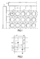
- Figure 1 shows a known pixel circuit for an active matrix addressed electroluminescent display device.
- the display device comprises a panel having a row and column matrix array of regularly-spaced pixels, denoted by the blocks 1 and comprising electroluminescent display elements 2 together with associated switching means, located at the intersections between crossing sets of row (selection) and column (data) address conductors 4 and 6. Only a few pixels are shown in the Figure for simplicity. In practice there may be several hundred rows and columns of pixels.
- the pixels 1 are addressed via the sets of row and column address conductors by a peripheral drive circuit comprising a row, scanning, driver circuit 8 and a column, data, driver circuit 9 connected to the ends of the respective sets of conductors.
- the electroluminescent display element 2 comprises an organic light emitting diode, represented here as a diode element (LED) and comprising a pair of electrodes between which one or more active layers of organic electroluminescent material is sandwiched.
- the display elements of the array are carried together with the associated active matrix circuitry on one side of an insulating support. Either the cathodes or the anodes of the display elements are formed of transparent conductive material.
- the support is of transparent material such as glass and the electrodes of the display elements 2 closest to the substrate may consist of a transparent conductive material such as ITO so that light generated by the electroluminescent layer is transmitted through these electrodes and the support so as to be visible to a viewer at the other side of the support.
- the thickness of the organic electroluminescent material layer is between 100 nm and 200nm.
- suitable organic electroluminescent materials which can be used for the elements 2 are known and described in EP-A-0 717446. Conjugated polymer materials as described in WO96/36959 can also be used.
- FIG. 2 shows in simplified schematic form a known pixel and drive circuitry arrangement.
- Each pixel 1 comprises the EL display element 2 and associated driver circuitry.
- the driver circuitry has an address transistor 16 which is turned on by a row address pulse on the row conductor 4.
- a voltage on the column conductor 6 can pass to the remainder of the pixel.
- the address transistor 16 supplies the column conductor voltage to a current source 20, which comprises a drive transistor 22 and a storage capacitor 24.
- the column voltage is provided to the gate of the drive transistor 22, and the gate is held at this voltage by the storage capacitor 24 even after the row address pulse has ended.
- the drive transistor 22 in this circuit is implemented as a PMOS TFT, so that the storage capacitor 24 holds the gate-source voltage fixed. This results in a fixed source-drain current through the transistor, which therefore provides the desired current source operation of the pixel.
- EP 1 220 191 discloses an electroluminescent display device in which each pixel has a drive transistor and a second transistor for compensating for a deviation in the threshold voltage of the drive transistor. A gate-source drive voltage for the drive transistor is held on a storage capacitor.
- an active matrix electroluminescent display device comprising an array of display pixels, each pixel comprising: an electroluminescent display element; an amorphous silicon or microcrystalline silicon first drive NMOS transistor connected between the anode of the display element and a power supply line; and a storage capacitor between the anode of the display element and the gate of the drive transistor, wherein each pixel further comprises an amorphous silicon or microcrystalline silicon second drive NMOS transistor for supplying a holding voltage to the anode of the display element.
- This arrangement enables the voltage across the display element to be held while the transistor gate drive voltage is stored on the storage capacitor.
- the drive transistor is an NMOS device
- the source is connected to the anode of the display element, so that this arrangement has the effect of holding the transistor source voltage to a known level while the drive voltage is stored on the storage capacitor. This enables an accurate current source pixel circuit to be implemented using NMOS transistors.
- the second drive transistor is preferably connected between the power supply line and the anode of the display element. In this way, the power supply line can supply both the holding voltage and the drive voltage for driving the display element.
- the second drive transistor can be connected between a second power supply line and the anode of the display element.
- This second power supply line can be shared between pixels in a row of the array.
- the gate of the first drive transistor may be coupled to a data signal line, for example a column conductor, through an address transistor driven by a row conductor.
- a pixel drive signal is thus coupled to the pixel in known manner.
- the first and second drive transistors are preferably microcrystalline silicon TFTs comprising silicon crystallites of size 40nm - 140nm in an amorphous silicon matrix. These transistors have improved carrier mobility and yet can still be deposited using a PECVD process. If the crystallites are large enough, then extended state conduction is enhanced and the mobility increased, approximately by a factor of 10 compared to amorphous silicon layers.
- the invention also provides a method of driving the pixels of an active matrix electroluminescent display device comprising an array of display pixels each having an electroluminescent display element, -the method comprising:
- a holding voltage is applied to the so that the source of the drive transistor is held at a fixed potential, so that a desired gate-source voltage can be accurately stored on a storage capacitor.
- the desired source-drain current is then driven through the second transistor by applying a first power supply voltage to the second transistor.
- amorphous or microcrystalline silicon transistors are used within the pixel structure. This requires the TFTs to be NMOS devices, as explained above.
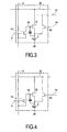
- Figure 3 shows a first example of pixel layout of the invention.
- the same reference numerals are used to denote the same components as in Figure 2, and the pixel circuit is for use in a display such as shown in Figure 1.
- the drive transistor 22 is implemented as an amorphous silicon or microcrystalline silicon NMOS TFT.
- the pixel circuitry is provided on a substrate on the anode side of the EL display element 2, and the source of the NMOS drive transistor is thus in electrical contact with anode of the EL display element.
- the storage capacitor 24 is provided between the anode of the display element 2 and the gate of the drive transistor 22 and is thereby charged to the gate-source voltage of the drive transistor 22 when it is addressed.
- the potential of the source may vary so that a given voltage from the column conductor 6 will not necessarily result in the same gate-source voltage stored on the storage capacitor 24.
- the pixel circuit of the invention includes a second drive NMOS transistor 30 for supplying a holding voltage to the anode of the display element 2. This holding voltage is supplied when the gate-source voltage is being transferred to the storage capacitor 24.
- the second drive transistor 30 is connected between a second power supply line 32 and the anode of the display element 2.
- the second power supply line 32 is shared between pixels in a row of the array, and the second drive transistor is controlled by a gate line 34 which is also shared between pixels in a row. This arrangement thus requires two additional row conductors, in addition to the row conductor 4.
- the second drive transistor 30 is turned on to hold the anode of the EL display element to the voltage on the second power supply line (less any source-drain voltage drop).
- the signal data voltage on the column conductor 6 then charges the storage capacitor 24 to a known gate-source voltage which corresponds to the desired source-drain current of the first drive transistor 22, which in turn corresponds to the desired level of illumination of the EL display element 2.
- the row conductor 4 is brought low to turn off the address transistor 16, and subsequently the gate line 34 is brought low, thereby allowing potential on the EL display element anode to vary. As this potential varies, the gate voltage varies as the gate-source voltage is preserved by the storage capacitor 24.
- This circuit requires the transistor 30 to be large so that all current from the drive transistor 22 can be directed to the second power supply line 32 without any voltage drop.
- a large additional transistor can use pixel aperture, and Figure 4 shows an alternative pixel configuration to avoid the need for the second drive transistor 30 to pass large currents.
- the second drive transistor 30 is connected between the (only) power supply line 26 and the anode of the display element 2. This reduces the current requirements of the second drive transistor 30.
- the power supply line 26 is held at a low potential so that the first drive transistor 22 does not conduct.
- the second drive transistor 30 is required only to discharge any residual charge on the EL display element 2 and to provide a charging path for the storage capacitor 24.
- the power supply line 26 is held low while all pixels are addressed. When addressing is finished, all address lines (row conductor 4 and gate lines 34) are brought low and the power supply line 26 is then brought high so that the LEDs light up.
- the flashing of the power supply line 26 will have the advantage of reduced sample and hold for motion blur reduction.
- the row conductors 4 and the gate lines 34 may be connected together so that no increase in the number of row conductors is required.
- the power supply line 26 can be modulated on a row-by-row basis or on an image-by-image basis.
- all transistors are NMOS transistors, which may be formed from amorphous silicon.
- NMOS transistors which may be formed from amorphous silicon.
- a preferred technology is microcrystalline silicon TFTs. These comprise silicon crystallites of size 40nm - 140nm in an amorphous silicon matrix.
- the EL display element may be any known organic EL display element, including polymer EL display elements.
- pixel layouts are addressed using a method by which a voltage across the display element is held during an addressing phase, which in turn holds the source voltage of the drive transistor. While this source voltage is held, a desired gate-source voltage is stored on the storage capacitor corresponding to a desired source-drain current for driving the display element. The holding voltage is then removed from the display element and the desired source-drain current is driven through the electroluminescent display element.
Landscapes
- Engineering & Computer Science (AREA)
- Physics & Mathematics (AREA)
- Computer Hardware Design (AREA)
- General Physics & Mathematics (AREA)
- Theoretical Computer Science (AREA)
- Control Of Indicators Other Than Cathode Ray Tubes (AREA)
- Control Of El Displays (AREA)
- Electroluminescent Light Sources (AREA)
- Illuminated Signs And Luminous Advertising (AREA)
- Thin Film Transistor (AREA)
Claims (13)
- Aktivmatrix-Elektrolumineszenzanzeigeeinrichtung mit einer Matrix von Anzeigepixeln (1), wobei jedes Pixel aufweist:- ein Elektrolumineszenzanzeigeelement (2) mit einer Anode,- einen ersten NMOS-Treibertransistor (22) aus amorphem Silicium oder mikrokristallinem Silicium, welcher mit einer Elektrode des Anzeigeelements (2) verbunden ist,- einen Speicherkondensator (24), welcher mit dem Gate des ersten NMOS-Treibertransistors (22) verbunden ist, sowie- einen zweiten NMOS-Treibertransistor (30) aus amorphem Silicium oder mikrokristallinem Silicium,dadurch gekennzeichnet, dass- der erste NMOS-Treibertransistor zwischen der Anode des Anzeigeelements (2) und einer Energieversorgungsleitung (26) geschaltet ist,- der Speicherkondensator (24) zwischen der Anode des Anzeigeelements (2) und dem Gate des Treibertransistors (22) geschaltet ist, und- der zweite NMOS-Treibertransistor (30) vorgesehen ist, um der Anode des Anzeigeelements (2) eine Haltespannung zuzuführen.
- Einrichtung nach Anspruch 1, wobei der zweite Treibertransistor (30) zwischen der Energieversorgungsleitung (26) und der Anode des Anzeigeelements (2) geschaltet ist.
- Einrichtung nach Anspruch 1, wobei der zweite Treibertransistor (30) zwischen einer zweiten Energieversorgungsleitung (32) und der Anode des Anzeigeelements (2) geschaltet ist.
- Einrichtung nach Anspruch 3, wobei die Matrix von Anzeigepixeln gegenüber der normalen Betrachtungsorientierung der Anzeige Zeilen und Spalten von Pixeln aufweist und die zweite Energieversorgungsleitung (32) zwischen Pixeln in einer Zeile der Matrix aufgeteilt ist.
- Einrichtung nach einem der vorangegangenen Ansprüche, wobei das Gate des ersten Treibertransistors (22) durch einen Adresstransistor (16) mit einer Datensignalleitung (6) verbunden ist.
- Einrichtung nach Anspruch 5, wobei die Matrix von Anzeigepixeln gegenüber der normalen Betrachtungsorientierung der Anzeige Zeilen und Spalten von Pixeln aufweist und die Datensignalleitung (6) einen Spaltenleiter aufweist, welcher zwischen Pixeln in einer Spalte der Matrix aufgeteilt ist.
- Einrichtung nach Anspruch 5 oder 6, wobei die Matrix von Anzeigepixeln gegenüber der normalen Betrachtungsorientierung der Anzeige Zeilen und Spalten von Pixeln aufweist und das Gate des Adresstransistors (16) mit einem Zeilenleiter (4) verbunden ist, welcher zwischen Pixeln in einer Zeile der Matrix aufgeteilt ist.
- Einrichtung nach einem der vorangegangenen Ansprüche, wobei der erste und der zweite Treibertransistor (22, 30) TFTs aus mikrokristallinem Silicium mit Siliciumkristalliten in der Größe zwischen 40 nm und 140 nm in einer Matrix aus amorphem Silicium aufweisen.
- Verfahren zur Steuerung der Pixel einer Aktivmatrix-Elektrolumineszenzanzeigeeinrichtung mit einer Matrix von Anzeigepixeln (1), welche jeweils- ein Elektrolumineszenzanzeigeelement (2) mit einer Anode,- einen ersten NMOS-Treibertransistor (22) aus amorphem Silicium oder mikrokristallinem Silicium,- einen zweiten NMOS-Treibertransistor (30) aus amorphem Silicium oder mikrokristallinem Silicium, welcher mit einer Elektrode des Anzeigeelements (2) verbunden ist, sowie- einen Speicherkondensator (24), welcher mit dem Gate des ersten NMOS-Treibertransistors (22) verbunden ist, aufweisen, dadurch gekennzeichnet, dass nach dem Verfahren:- die Spannung an dem Anzeigeelement (2) gehalten wird, indem durch den ersten NMOS-Transistor (22) aus amorphem Silicium oder mikrokristallinem Silicium eine Haltespannung angelegt wird, wobei die Haltespannung die Sourcespannung des zwischen der Anode des Anzeigeelements (2) und einer Energieversorgungsleitung (26) geschalteten, zweiten NMOS-Transistors (30) aus amorphem Silicium oder mikrokristallinem Silicium hält,- während des Haltens der Spannung an dem Anzeigeelement (2) eine gewünschte Gate-Source-Spannung auf dem zwischen dem Gate und der Source des zweiten Transistors (30) geschalteten Speicherkondensator (24) gespeichert wird, wobei die Gate-Source-Spannung einem gewünschten Source-Drain-Strom zur Steuerung des Anzeigeelements (2) entspricht,- die Haltespannung von dem Anzeigeelement (2) weggenommen wird und- der gewünschte Source-Drain-Strom durch das Elektrolumineszenzanzeigeelement (2) gesteuert wird.
- Verfahren nach Anspruch 9, wobei der gewünschte Source-Drain-Strom durch den zweiten Transistor (30) durch Anlegen einer ersten Versorgungsspannung (26) an den zweiten Transistor (30) gesteuert wird.
- Verfahren nach Anspruch 10, wobei die erste Versorgungsspannung nicht an den zweiten Transistor angelegt wird, während die Spannung an dem Anzeigeelement gehalten wird.
- Verfahren nach Anspruch 11, wobei die erste Versorgungsspannung und die Haltespannung durch eine gemeinsame Energieversorgungsleitung (26) abgegeben werden.
- Verfahren nach einem der Ansprüche 9 bis 12, wonach die Speicherung einer gewünschten Gate-Source-Spannung auf einem Speicherkondensator (24) die Kopplung von Daten von einer Datensignalleitung (6) mit dem Speicherkondensator (24) durch einen Adresstransistor (16) umfasst.
Applications Claiming Priority (3)
| Application Number | Priority Date | Filing Date | Title |
|---|---|---|---|
| GB0218170 | 2002-08-06 | ||
| GBGB0218170.9A GB0218170D0 (en) | 2002-08-06 | 2002-08-06 | Electroluminescent display devices |
| PCT/IB2003/003202 WO2004015667A1 (en) | 2002-08-06 | 2003-07-22 | Electroluminescent display device having pixels with nmos transistors |
Publications (2)
| Publication Number | Publication Date |
|---|---|
| EP1529276A1 EP1529276A1 (de) | 2005-05-11 |
| EP1529276B1 true EP1529276B1 (de) | 2006-07-05 |
Family
ID=9941770
Family Applications (1)
| Application Number | Title | Priority Date | Filing Date |
|---|---|---|---|
| EP03784336A Expired - Lifetime EP1529276B1 (de) | 2002-08-06 | 2003-07-22 | Elektrolumineszenzanzeigebauelement mit pixeln mit nmos-transistoren |
Country Status (11)
| Country | Link |
|---|---|
| US (1) | US8624803B2 (de) |
| EP (1) | EP1529276B1 (de) |
| JP (1) | JP2005534990A (de) |
| KR (1) | KR20050035253A (de) |
| CN (1) | CN100378786C (de) |
| AT (1) | ATE332557T1 (de) |
| AU (1) | AU2003247058A1 (de) |
| DE (1) | DE60306656T2 (de) |
| GB (1) | GB0218170D0 (de) |
| TW (1) | TW200405255A (de) |
| WO (1) | WO2004015667A1 (de) |
Cited By (1)
| Publication number | Priority date | Publication date | Assignee | Title |
|---|---|---|---|---|
| US9805649B2 (en) | 2013-08-05 | 2017-10-31 | Samsung Display Co., Ltd. | Display device and driving method thereof |
Families Citing this family (16)
| Publication number | Priority date | Publication date | Assignee | Title |
|---|---|---|---|---|
| US8937580B2 (en) * | 2003-08-08 | 2015-01-20 | Semiconductor Energy Laboratory Co., Ltd. | Driving method of light emitting device and light emitting device |
| JP4687943B2 (ja) * | 2004-03-18 | 2011-05-25 | 奇美電子股▲ふん▼有限公司 | 画像表示装置 |
| US7317433B2 (en) | 2004-07-16 | 2008-01-08 | E.I. Du Pont De Nemours And Company | Circuit for driving an electronic component and method of operating an electronic device having the circuit |
| US7317434B2 (en) * | 2004-12-03 | 2008-01-08 | Dupont Displays, Inc. | Circuits including switches for electronic devices and methods of using the electronic devices |
| CA2490858A1 (en) * | 2004-12-07 | 2006-06-07 | Ignis Innovation Inc. | Driving method for compensated voltage-programming of amoled displays |
| KR100623813B1 (ko) * | 2004-12-10 | 2006-09-19 | 엘지.필립스 엘시디 주식회사 | 유기전계발광 소자 및 그 구동방법 |
| EP1873746A1 (de) * | 2006-06-30 | 2008-01-02 | Deutsche Thomson-Brandt Gmbh | Verfahren und Vorrichtung zur Ansteuerung eines AMOLED mit variabler Steuerspannung |
| EP1887549A3 (de) * | 2006-06-30 | 2009-03-18 | Thomson Licensing | Verfahren und Vorrichtung zur Ansteuerung eines AMOLED mit variabler Steuerspannung |
| JP5503255B2 (ja) | 2009-11-10 | 2014-05-28 | グローバル・オーエルイーディー・テクノロジー・リミテッド・ライアビリティ・カンパニー | 画素回路、表示装置および検査方法 |
| WO2013094422A1 (ja) * | 2011-12-21 | 2013-06-27 | シャープ株式会社 | 画素回路及び表示装置 |
| US9443469B2 (en) | 2013-11-22 | 2016-09-13 | Global Oled Technology Llc | Pixel circuit, driving method, display device, and inspection method |
| JPWO2020148958A1 (ja) * | 2019-01-16 | 2021-12-02 | ソニーセミコンダクタソリューションズ株式会社 | 電気光学装置及び電子機器 |
| CN110491334B (zh) * | 2019-08-30 | 2021-07-23 | 上海中航光电子有限公司 | 像素电路、像素电路的驱动方法、显示面板和显示装置 |
| CN110473494B (zh) * | 2019-08-30 | 2021-07-09 | 上海中航光电子有限公司 | 一种像素电路、显示面板和像素电路的驱动方法 |
| CN114783375B (zh) * | 2022-03-31 | 2023-09-26 | 深圳市华星光电半导体显示技术有限公司 | 像素驱动电路、像素驱动方法和显示面板 |
| CN115966176B (zh) * | 2022-12-28 | 2024-02-09 | 惠科股份有限公司 | 阵列基板和显示面板 |
Family Cites Families (29)
| Publication number | Priority date | Publication date | Assignee | Title |
|---|---|---|---|---|
| JPH113048A (ja) * | 1997-06-10 | 1999-01-06 | Canon Inc | エレクトロ・ルミネセンス素子及び装置、並びにその製造法 |
| GB9812742D0 (en) * | 1998-06-12 | 1998-08-12 | Philips Electronics Nv | Active matrix electroluminescent display devices |
| JP4493741B2 (ja) * | 1998-09-04 | 2010-06-30 | 株式会社半導体エネルギー研究所 | 半導体装置の作製方法 |
| JP2000284749A (ja) * | 1999-03-30 | 2000-10-13 | Dainippon Printing Co Ltd | 画像表示装置 |
| JP4092857B2 (ja) * | 1999-06-17 | 2008-05-28 | ソニー株式会社 | 画像表示装置 |
| EP1130565A4 (de) * | 1999-07-14 | 2006-10-04 | Sony Corp | Stromsteuerschaltung und anzeigevorrichtung damit, bildpunktschaltung und ansteuerverfahren |
| TW587239B (en) * | 1999-11-30 | 2004-05-11 | Semiconductor Energy Lab | Electric device |
| TW493152B (en) * | 1999-12-24 | 2002-07-01 | Semiconductor Energy Lab | Electronic device |
| KR100327374B1 (ko) * | 2000-03-06 | 2002-03-06 | 구자홍 | 액티브 구동 회로 |
| US20010030511A1 (en) * | 2000-04-18 | 2001-10-18 | Shunpei Yamazaki | Display device |
| TWI292143B (en) * | 2000-07-07 | 2008-01-01 | Seiko Epson Corp | Circuit, driver circuit, organic electroluminescent display device electro-optical device, electronic apparatus, method of controlling the current supply to an organic electroluminescent pixel, and method for driving a circuit |
| KR100370286B1 (ko) * | 2000-12-29 | 2003-01-29 | 삼성에스디아이 주식회사 | 전압구동 유기발광소자의 픽셀회로 |
| US7061451B2 (en) * | 2001-02-21 | 2006-06-13 | Semiconductor Energy Laboratory Co., Ltd, | Light emitting device and electronic device |
| JP4869497B2 (ja) * | 2001-05-30 | 2012-02-08 | 株式会社半導体エネルギー研究所 | 表示装置 |
| US6734636B2 (en) * | 2001-06-22 | 2004-05-11 | International Business Machines Corporation | OLED current drive pixel circuit |
| JP3800050B2 (ja) * | 2001-08-09 | 2006-07-19 | 日本電気株式会社 | 表示装置の駆動回路 |
| US6876350B2 (en) * | 2001-08-10 | 2005-04-05 | Semiconductor Energy Laboratory Co., Ltd. | Display device and electronic equipment using the same |
| JP4052865B2 (ja) * | 2001-09-28 | 2008-02-27 | 三洋電機株式会社 | 半導体装置及び表示装置 |
| JP2003208127A (ja) * | 2001-11-09 | 2003-07-25 | Sanyo Electric Co Ltd | 表示装置 |
| JP4485119B2 (ja) * | 2001-11-13 | 2010-06-16 | 株式会社半導体エネルギー研究所 | 表示装置 |
| US7071932B2 (en) * | 2001-11-20 | 2006-07-04 | Toppoly Optoelectronics Corporation | Data voltage current drive amoled pixel circuit |
| GB0130176D0 (en) * | 2001-12-18 | 2002-02-06 | Koninkl Philips Electronics Nv | Electroluminescent display device |
| JP2003186437A (ja) * | 2001-12-18 | 2003-07-04 | Sanyo Electric Co Ltd | 表示装置 |
| TW540025B (en) * | 2002-02-04 | 2003-07-01 | Au Optronics Corp | Driving circuit of display |
| JP3613253B2 (ja) * | 2002-03-14 | 2005-01-26 | 日本電気株式会社 | 電流制御素子の駆動回路及び画像表示装置 |
| JP3750616B2 (ja) * | 2002-03-05 | 2006-03-01 | 日本電気株式会社 | 画像表示装置及び該画像表示装置に用いられる制御方法 |
| JP2004029247A (ja) * | 2002-06-24 | 2004-01-29 | Nippon Hoso Kyokai <Nhk> | 発光素子の駆動回路及び画像表示装置 |
| DE10254511B4 (de) * | 2002-11-22 | 2008-06-05 | Universität Stuttgart | Aktiv-Matrix-Ansteuerschaltung |
| TW589754B (en) * | 2003-05-12 | 2004-06-01 | Au Optronics Corp | Active organic electroluminescent display unit |
-
2002
- 2002-08-06 GB GBGB0218170.9A patent/GB0218170D0/en not_active Ceased
-
2003
- 2003-07-22 EP EP03784336A patent/EP1529276B1/de not_active Expired - Lifetime
- 2003-07-22 CN CNB038186586A patent/CN100378786C/zh not_active Expired - Fee Related
- 2003-07-22 WO PCT/IB2003/003202 patent/WO2004015667A1/en not_active Ceased
- 2003-07-22 AU AU2003247058A patent/AU2003247058A1/en not_active Abandoned
- 2003-07-22 DE DE60306656T patent/DE60306656T2/de not_active Expired - Fee Related
- 2003-07-22 KR KR1020057001916A patent/KR20050035253A/ko not_active Ceased
- 2003-07-22 AT AT03784336T patent/ATE332557T1/de not_active IP Right Cessation
- 2003-07-22 US US10/523,379 patent/US8624803B2/en active Active
- 2003-07-22 JP JP2004527148A patent/JP2005534990A/ja active Pending
- 2003-08-01 TW TW092121157A patent/TW200405255A/zh unknown
Cited By (1)
| Publication number | Priority date | Publication date | Assignee | Title |
|---|---|---|---|---|
| US9805649B2 (en) | 2013-08-05 | 2017-10-31 | Samsung Display Co., Ltd. | Display device and driving method thereof |
Also Published As
| Publication number | Publication date |
|---|---|
| EP1529276A1 (de) | 2005-05-11 |
| US20060113919A1 (en) | 2006-06-01 |
| JP2005534990A (ja) | 2005-11-17 |
| ATE332557T1 (de) | 2006-07-15 |
| AU2003247058A1 (en) | 2004-02-25 |
| TW200405255A (en) | 2004-04-01 |
| DE60306656D1 (de) | 2006-08-17 |
| KR20050035253A (ko) | 2005-04-15 |
| CN100378786C (zh) | 2008-04-02 |
| CN1675669A (zh) | 2005-09-28 |
| WO2004015667A1 (en) | 2004-02-19 |
| US8624803B2 (en) | 2014-01-07 |
| DE60306656T2 (de) | 2007-06-21 |
| GB0218170D0 (en) | 2002-09-11 |
Similar Documents
| Publication | Publication Date | Title |
|---|---|---|
| US8624803B2 (en) | Electroluminescent display device having pixels with NMOS transistors | |
| US7719492B2 (en) | Threshold voltage compensation method for electroluminescent display devices | |
| US7800565B2 (en) | Method and system for programming and driving active matrix light emitting device pixel | |
| US7956826B2 (en) | Electroluminescent display device to display low brightness uniformly | |
| EP1704554B1 (de) | Elektrolumineszenz-display-einrichtungen mit einer aktivmatrix | |
| US7619593B2 (en) | Active matrix display device | |
| US7924247B2 (en) | Display device and driving method thereof | |
| US7872626B2 (en) | System and method for dynamically calibrating driver circuits in a display device | |
| KR20060136392A (ko) | 전계 발광 디스플레이 디바이스를 위한 임계전압 보상 방법 | |
| KR20050110961A (ko) | 표시 장치 및 그 구동 방법 | |
| JP2005538403A (ja) | エレクトロルミネセント表示装置 | |
| US7109522B2 (en) | Electroluminescent display devices | |
| WO2007049182A2 (en) | Active matrix display devices | |
| KR20090026907A (ko) | 유기전계발광표시장치 |
Legal Events
| Date | Code | Title | Description |
|---|---|---|---|
| PUAI | Public reference made under article 153(3) epc to a published international application that has entered the european phase |
Free format text: ORIGINAL CODE: 0009012 |
|
| 17P | Request for examination filed |
Effective date: 20050307 |
|
| AK | Designated contracting states |
Kind code of ref document: A1 Designated state(s): AT BE BG CH CY CZ DE DK EE ES FI FR GB GR HU IE IT LI LU MC NL PT RO SE SI SK TR |
|
| AX | Request for extension of the european patent |
Extension state: AL LT LV MK |
|
| 17Q | First examination report despatched |
Effective date: 20050525 |
|
| DAX | Request for extension of the european patent (deleted) | ||
| GRAP | Despatch of communication of intention to grant a patent |
Free format text: ORIGINAL CODE: EPIDOSNIGR1 |
|
| GRAC | Information related to communication of intention to grant a patent modified |
Free format text: ORIGINAL CODE: EPIDOSCIGR1 |
|
| GRAS | Grant fee paid |
Free format text: ORIGINAL CODE: EPIDOSNIGR3 |
|
| GRAA | (expected) grant |
Free format text: ORIGINAL CODE: 0009210 |
|
| AK | Designated contracting states |
Kind code of ref document: B1 Designated state(s): AT BE BG CH CY CZ DE DK EE ES FI FR GB GR HU IE IT LI LU MC NL PT RO SE SI SK TR |
|
| PG25 | Lapsed in a contracting state [announced via postgrant information from national office to epo] |
Ref country code: AT Free format text: LAPSE BECAUSE OF FAILURE TO SUBMIT A TRANSLATION OF THE DESCRIPTION OR TO PAY THE FEE WITHIN THE PRESCRIBED TIME-LIMIT Effective date: 20060705 Ref country code: NL Free format text: LAPSE BECAUSE OF FAILURE TO SUBMIT A TRANSLATION OF THE DESCRIPTION OR TO PAY THE FEE WITHIN THE PRESCRIBED TIME-LIMIT Effective date: 20060705 Ref country code: BE Free format text: LAPSE BECAUSE OF FAILURE TO SUBMIT A TRANSLATION OF THE DESCRIPTION OR TO PAY THE FEE WITHIN THE PRESCRIBED TIME-LIMIT Effective date: 20060705 Ref country code: IT Free format text: LAPSE BECAUSE OF FAILURE TO SUBMIT A TRANSLATION OF THE DESCRIPTION OR TO PAY THE FEE WITHIN THE PRESCRIBED TIME-LIMIT;WARNING: LAPSES OF ITALIAN PATENTS WITH EFFECTIVE DATE BEFORE 2007 MAY HAVE OCCURRED AT ANY TIME BEFORE 2007. THE CORRECT EFFECTIVE DATE MAY BE DIFFERENT FROM THE ONE RECORDED. Effective date: 20060705 Ref country code: CZ Free format text: LAPSE BECAUSE OF FAILURE TO SUBMIT A TRANSLATION OF THE DESCRIPTION OR TO PAY THE FEE WITHIN THE PRESCRIBED TIME-LIMIT Effective date: 20060705 Ref country code: SI Free format text: LAPSE BECAUSE OF FAILURE TO SUBMIT A TRANSLATION OF THE DESCRIPTION OR TO PAY THE FEE WITHIN THE PRESCRIBED TIME-LIMIT Effective date: 20060705 Ref country code: RO Free format text: LAPSE BECAUSE OF FAILURE TO SUBMIT A TRANSLATION OF THE DESCRIPTION OR TO PAY THE FEE WITHIN THE PRESCRIBED TIME-LIMIT Effective date: 20060705 Ref country code: CH Free format text: LAPSE BECAUSE OF FAILURE TO SUBMIT A TRANSLATION OF THE DESCRIPTION OR TO PAY THE FEE WITHIN THE PRESCRIBED TIME-LIMIT Effective date: 20060705 Ref country code: FI Free format text: LAPSE BECAUSE OF FAILURE TO SUBMIT A TRANSLATION OF THE DESCRIPTION OR TO PAY THE FEE WITHIN THE PRESCRIBED TIME-LIMIT Effective date: 20060705 Ref country code: SK Free format text: LAPSE BECAUSE OF FAILURE TO SUBMIT A TRANSLATION OF THE DESCRIPTION OR TO PAY THE FEE WITHIN THE PRESCRIBED TIME-LIMIT Effective date: 20060705 Ref country code: LI Free format text: LAPSE BECAUSE OF FAILURE TO SUBMIT A TRANSLATION OF THE DESCRIPTION OR TO PAY THE FEE WITHIN THE PRESCRIBED TIME-LIMIT Effective date: 20060705 |
|
| REG | Reference to a national code |
Ref country code: GB Ref legal event code: FG4D |
|
| REG | Reference to a national code |
Ref country code: CH Ref legal event code: EP |
|
| PG25 | Lapsed in a contracting state [announced via postgrant information from national office to epo] |
Ref country code: IE Free format text: LAPSE BECAUSE OF NON-PAYMENT OF DUE FEES Effective date: 20060724 |
|
| PG25 | Lapsed in a contracting state [announced via postgrant information from national office to epo] |
Ref country code: MC Free format text: LAPSE BECAUSE OF NON-PAYMENT OF DUE FEES Effective date: 20060731 |
|
| REG | Reference to a national code |
Ref country code: IE Ref legal event code: FG4D |
|
| REF | Corresponds to: |
Ref document number: 60306656 Country of ref document: DE Date of ref document: 20060817 Kind code of ref document: P |
|
| PG25 | Lapsed in a contracting state [announced via postgrant information from national office to epo] |
Ref country code: DK Free format text: LAPSE BECAUSE OF FAILURE TO SUBMIT A TRANSLATION OF THE DESCRIPTION OR TO PAY THE FEE WITHIN THE PRESCRIBED TIME-LIMIT Effective date: 20061005 Ref country code: SE Free format text: LAPSE BECAUSE OF FAILURE TO SUBMIT A TRANSLATION OF THE DESCRIPTION OR TO PAY THE FEE WITHIN THE PRESCRIBED TIME-LIMIT Effective date: 20061005 Ref country code: BG Free format text: LAPSE BECAUSE OF FAILURE TO SUBMIT A TRANSLATION OF THE DESCRIPTION OR TO PAY THE FEE WITHIN THE PRESCRIBED TIME-LIMIT Effective date: 20061005 |
|
| PG25 | Lapsed in a contracting state [announced via postgrant information from national office to epo] |
Ref country code: ES Free format text: LAPSE BECAUSE OF FAILURE TO SUBMIT A TRANSLATION OF THE DESCRIPTION OR TO PAY THE FEE WITHIN THE PRESCRIBED TIME-LIMIT Effective date: 20061016 |
|
| NLV1 | Nl: lapsed or annulled due to failure to fulfill the requirements of art. 29p and 29m of the patents act | ||
| PG25 | Lapsed in a contracting state [announced via postgrant information from national office to epo] |
Ref country code: PT Free format text: LAPSE BECAUSE OF FAILURE TO SUBMIT A TRANSLATION OF THE DESCRIPTION OR TO PAY THE FEE WITHIN THE PRESCRIBED TIME-LIMIT Effective date: 20061205 |
|
| ET | Fr: translation filed | ||
| PLBE | No opposition filed within time limit |
Free format text: ORIGINAL CODE: 0009261 |
|
| STAA | Information on the status of an ep patent application or granted ep patent |
Free format text: STATUS: NO OPPOSITION FILED WITHIN TIME LIMIT |
|
| 26N | No opposition filed |
Effective date: 20070410 |
|
| PG25 | Lapsed in a contracting state [announced via postgrant information from national office to epo] |
Ref country code: GR Free format text: LAPSE BECAUSE OF FAILURE TO SUBMIT A TRANSLATION OF THE DESCRIPTION OR TO PAY THE FEE WITHIN THE PRESCRIBED TIME-LIMIT Effective date: 20061006 |
|
| PG25 | Lapsed in a contracting state [announced via postgrant information from national office to epo] |
Ref country code: EE Free format text: LAPSE BECAUSE OF FAILURE TO SUBMIT A TRANSLATION OF THE DESCRIPTION OR TO PAY THE FEE WITHIN THE PRESCRIBED TIME-LIMIT Effective date: 20060705 |
|
| PG25 | Lapsed in a contracting state [announced via postgrant information from national office to epo] |
Ref country code: TR Free format text: LAPSE BECAUSE OF FAILURE TO SUBMIT A TRANSLATION OF THE DESCRIPTION OR TO PAY THE FEE WITHIN THE PRESCRIBED TIME-LIMIT Effective date: 20060705 Ref country code: LU Free format text: LAPSE BECAUSE OF NON-PAYMENT OF DUE FEES Effective date: 20060722 Ref country code: HU Free format text: LAPSE BECAUSE OF FAILURE TO SUBMIT A TRANSLATION OF THE DESCRIPTION OR TO PAY THE FEE WITHIN THE PRESCRIBED TIME-LIMIT Effective date: 20070106 |
|
| PGFP | Annual fee paid to national office [announced via postgrant information from national office to epo] |
Ref country code: DE Payment date: 20080904 Year of fee payment: 6 |
|
| PG25 | Lapsed in a contracting state [announced via postgrant information from national office to epo] |
Ref country code: CY Free format text: LAPSE BECAUSE OF FAILURE TO SUBMIT A TRANSLATION OF THE DESCRIPTION OR TO PAY THE FEE WITHIN THE PRESCRIBED TIME-LIMIT Effective date: 20060705 |
|
| PGFP | Annual fee paid to national office [announced via postgrant information from national office to epo] |
Ref country code: GB Payment date: 20080828 Year of fee payment: 6 |
|
| PGFP | Annual fee paid to national office [announced via postgrant information from national office to epo] |
Ref country code: FR Payment date: 20090730 Year of fee payment: 7 |
|
| GBPC | Gb: european patent ceased through non-payment of renewal fee |
Effective date: 20090722 |
|
| PG25 | Lapsed in a contracting state [announced via postgrant information from national office to epo] |
Ref country code: GB Free format text: LAPSE BECAUSE OF NON-PAYMENT OF DUE FEES Effective date: 20090722 |
|
| PG25 | Lapsed in a contracting state [announced via postgrant information from national office to epo] |
Ref country code: DE Free format text: LAPSE BECAUSE OF NON-PAYMENT OF DUE FEES Effective date: 20100202 |
|
| REG | Reference to a national code |
Ref country code: FR Ref legal event code: ST Effective date: 20110331 |
|
| PG25 | Lapsed in a contracting state [announced via postgrant information from national office to epo] |
Ref country code: FR Free format text: LAPSE BECAUSE OF NON-PAYMENT OF DUE FEES Effective date: 20100802 |