EP1528596A1 - Dispositif de retenue pour au moins un empilement de semiconducteurs ainsi qu' un système électrique pourvu d'un tel dispositif - Google Patents
Dispositif de retenue pour au moins un empilement de semiconducteurs ainsi qu' un système électrique pourvu d'un tel dispositif Download PDFInfo
- Publication number
- EP1528596A1 EP1528596A1 EP03405766A EP03405766A EP1528596A1 EP 1528596 A1 EP1528596 A1 EP 1528596A1 EP 03405766 A EP03405766 A EP 03405766A EP 03405766 A EP03405766 A EP 03405766A EP 1528596 A1 EP1528596 A1 EP 1528596A1
- Authority
- EP
- European Patent Office
- Prior art keywords
- semiconductor
- side part
- holding device
- holding devices
- semiconductor stacking
- Prior art date
- Legal status (The legal status is an assumption and is not a legal conclusion. Google has not performed a legal analysis and makes no representation as to the accuracy of the status listed.)
- Withdrawn
Links
Images



Classifications
-
- H—ELECTRICITY
- H10—SEMICONDUCTOR DEVICES; ELECTRIC SOLID-STATE DEVICES NOT OTHERWISE PROVIDED FOR
- H10W—GENERIC PACKAGES, INTERCONNECTIONS, CONNECTORS OR OTHER CONSTRUCTIONAL DETAILS OF DEVICES COVERED BY CLASS H10
- H10W90/00—Package configurations
-
- H—ELECTRICITY
- H10—SEMICONDUCTOR DEVICES; ELECTRIC SOLID-STATE DEVICES NOT OTHERWISE PROVIDED FOR
- H10W—GENERIC PACKAGES, INTERCONNECTIONS, CONNECTORS OR OTHER CONSTRUCTIONAL DETAILS OF DEVICES COVERED BY CLASS H10
- H10W40/00—Arrangements for thermal protection or thermal control
- H10W40/60—Securing means for detachable heating or cooling arrangements, e.g. clamps
- H10W40/611—Bolts or screws
- H10W40/613—Bolts or screws for stacked arrangements of a plurality of semiconductor devices
Definitions
- the present invention relates to the field of electronic fastening technology and power electronic components. It relates to a holding device for at least a stacked semiconductor stack and an electrical system having at least two Such holding devices according to the preamble of the independent claims.
- Such a holding device for at least one semiconductor stack is for example in DE 199 37 671 A1 disclosed. This is the holding device of a ceiling part, a bottom part and a first side part and a second side part constructed, wherein the ceiling part over the first and second side part is formed connectable to the bottom part and the or each Semiconductor stack is clamped between the top part and the bottom part. Furthermore are metallic guide elements on the semiconductor stack, in particular provided the heat sinks of the individual power semiconductors of the semiconductor stacking association, with which the semiconductor stacking band is guided on the two side parts.
- the object of the invention is therefore, a holding device for at least one semiconductor stack indicate at the partial discharges on the semiconductor stacking and / or can be largely avoided on the holding device.
- an electric Specify system which at least two inventive holding devices includes and has a space-saving design and virtually no partial discharges or only in very small numbers on the Halbleiterstapelverbitzen and / or on the Holding devices at the same time high switching currents or high switching voltages having.
- the inventive holding device for at least one semiconductor stack is from a ceiling part, a bottom part and a first side part and a second side part constructed, wherein the ceiling part via the first and second side part with the bottom part connectable formed and the or each semiconductor stacked between the ceiling part and the bottom part is clamped.
- the first side part and the second side part each non-contact of the or each semiconductor stacking spaced.
- each of the or each semiconductor stacked association is advantageously achieved that partial discharges on the first side part and / or on the second side part and / or on the corresponding one Semiconductor stacking, in particular during operation of the respective semiconductor stacking association
- partial discharges on the first side part and / or on the second side part and / or on the corresponding one Semiconductor stacking in particular during operation of the respective semiconductor stacking association
- no as known from the prior art touch one of the side parts or both sides is present with the Halbleiterstapel
- the electrical system according to the invention has at least two holding devices according to the invention, wherein the holding devices arranged side by side or one above the other are.
- inventive electrical system with an arrangement of the holding devices side by side can be advantageously achieved that very high switching currents, in particular in the case of parallel connection of all semiconductor stacking units, at the same time almost no or only a very small occurrence of partial discharges at the semiconductor stackings and / or can be achieved on the holding devices.
- the inventive electrical system with an arrangement of the holding devices one above the other advantageously be achieved that very high switching voltages, in particular with series connection of all semiconductor stackings, at the same time with almost no or only a very small occurrence of partial discharges at the semiconductor stackings and / or can be achieved on the holding devices.
- by the arrangement of the holding devices side by side or one above the other a very space-saving construction of the inventive reached electrical system.
- FIG. 1 shows a three-dimensional representation of a first embodiment of a holding device according to the invention for at least one semiconductor stacking device.
- the holding device according to the invention is constructed from a cover part 2, a bottom part 3 and a first side part 4 and a second side part 5.
- the ceiling part 2 is connected via the first and second side part 4, 5 connected to the bottom part 3 connectable.
- the or each semiconductor stack 1 is clamped between the top part 2 and the bottom part 3.
- the first side part 4 and the second side part 5 are each spaced from the semiconductor stack 1, in the case of a single stacked semiconductor stack 1, or from each stacked semiconductor stack 1, in the case of several semiconductor stackings 1.
- the two side parts 4, 5 or the power semiconductor switch of the associated semiconductor stacking device 1 are also advantageously protected against damage or destruction. Furthermore, by the above-mentioned spacing, a virtually unlimited switching voltage U s can be applied to the respective semiconductor stack 1 or a virtually unlimited switching current can be conducted.
- the first and second side part 4, 5 according to FIG. 1 and FIG. 2 are each plate-shaped designed so that a very space-saving design of the holding device achieved can be.
- the two side parts 4, 5 by their plate-like design be made very simple and inexpensive.
- a drive unit 7 and a circuit 8 for provided the corresponding semiconductor stack 1, preferably at the Insulating material containing first side plate 4 or on the insulating material containing second side plate 5 is arranged, whereby the drive unit 7 and the wiring 8 in a very simple manner with respect to the associated semiconductor stack 1 can be isolated.
- the first side plate 4 and / or the second side plate 5 as a fastening unit for fixing the drive unit 7 and / or the circuit 8, whereby the first and second side plate 4, 5 very can be easily prefabricated with the drive unit 7 and / or the circuit and to facilitate later maintenance on the entire holding device.
- the distance a of the first side part 4 to the semiconductor stack 1 and / or the distance a of the second side part 5 is selected to the semiconductor stack 1 each such that a As homogeneous as possible electric field between the semiconductor stack 1 and the first and second side part 4, 5 sets.
- the distance a of the first side part 4 to the first side part 4 nearest semiconductor stack 1 and / or the distance a of the second side part 5 to the second side part 5 nearest semiconductor stack 1 selected such that a possible homogeneous electric field between the respective semiconductor stacking 1 and the first and second side part 4, 5 sets.
- the clamping of the respective semiconductor stacking assembly 1 a clamping device 6 between the ceiling part 2 and the respective Semiconductor stacking 1 arranged, which the respective semiconductor stacking Association. 1 clamped between the top part 2 and the bottom part 3 and thus the semiconductors and Heatsink of the semiconductor stacking Association 1 thermally and electrically contacted. Furthermore is the respective semiconductor stack 1 in the installed state by the above described clamping device 6 protected against displacement and falling out.
- the clamping device 6 is designed as a spring.
- inventive holding device Due to the simple and space-saving design of the inventive holding device This can, for example, without cabinet and / or freestanding and / or suspended be used, so that a variety of additional uses the inventive holding device results in a variety of applications.
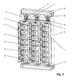
- FIG. 3 is a perspective view of a first embodiment of an inventive electrical system shown.
- This shows the inventive electrical system at least two examples described above with reference to FIG. 1 and FIG Inventive holding devices, wherein the holding devices arranged side by side are in Fig. 3 explicitly two inventive holding devices, each with a Semiconductor stacking Association 1 are shown.
- inventive electrical system with an arrangement of the holding devices side by side can be advantageously effected be that very high switching currents, especially in parallel all semiconductor stackings 1, with almost no or very little occurrence of Partial discharges on the Halbleiterstapelverbitzen 1 and / or on the holding devices are reachable.
- each one of the side parts 4, 5 saved be so that each two adjacent holding devices only a common Side part, as shown in Fig. 3, have.
Landscapes
- Power Conversion In General (AREA)
Priority Applications (1)
| Application Number | Priority Date | Filing Date | Title |
|---|---|---|---|
| EP03405766A EP1528596A1 (fr) | 2003-10-27 | 2003-10-27 | Dispositif de retenue pour au moins un empilement de semiconducteurs ainsi qu' un système électrique pourvu d'un tel dispositif |
Applications Claiming Priority (1)
| Application Number | Priority Date | Filing Date | Title |
|---|---|---|---|
| EP03405766A EP1528596A1 (fr) | 2003-10-27 | 2003-10-27 | Dispositif de retenue pour au moins un empilement de semiconducteurs ainsi qu' un système électrique pourvu d'un tel dispositif |
Publications (1)
| Publication Number | Publication Date |
|---|---|
| EP1528596A1 true EP1528596A1 (fr) | 2005-05-04 |
Family
ID=34400619
Family Applications (1)
| Application Number | Title | Priority Date | Filing Date |
|---|---|---|---|
| EP03405766A Withdrawn EP1528596A1 (fr) | 2003-10-27 | 2003-10-27 | Dispositif de retenue pour au moins un empilement de semiconducteurs ainsi qu' un système électrique pourvu d'un tel dispositif |
Country Status (1)
| Country | Link |
|---|---|
| EP (1) | EP1528596A1 (fr) |
Cited By (1)
| Publication number | Priority date | Publication date | Assignee | Title |
|---|---|---|---|---|
| WO2010145870A1 (fr) * | 2009-06-16 | 2010-12-23 | Abb Schweiz Ag | Unité électronique de puissance et système équipé desdites unités |
Citations (5)
| Publication number | Priority date | Publication date | Assignee | Title |
|---|---|---|---|---|
| DE19937671A1 (de) * | 1999-08-10 | 2001-02-22 | Siemens Ag | Luftgekühlte Stromrichter-Brückenschaltung |
| JP2001196535A (ja) * | 2000-01-11 | 2001-07-19 | Toshiba Corp | 平型半導体素子用スタック |
| EP1207553A1 (fr) * | 2000-11-16 | 2002-05-22 | ABB Schweiz AG | Dispositif de fixation pour une dispositif semi-conducteur à haut prestation avec des contacts par pression |
| JP2003168778A (ja) * | 2001-12-03 | 2003-06-13 | Toshiba Corp | 平型半導体素子用スタック |
| DE10164522A1 (de) * | 2001-12-17 | 2003-07-03 | Siemens Ag | Spannvorrichtung |
-
2003
- 2003-10-27 EP EP03405766A patent/EP1528596A1/fr not_active Withdrawn
Patent Citations (5)
| Publication number | Priority date | Publication date | Assignee | Title |
|---|---|---|---|---|
| DE19937671A1 (de) * | 1999-08-10 | 2001-02-22 | Siemens Ag | Luftgekühlte Stromrichter-Brückenschaltung |
| JP2001196535A (ja) * | 2000-01-11 | 2001-07-19 | Toshiba Corp | 平型半導体素子用スタック |
| EP1207553A1 (fr) * | 2000-11-16 | 2002-05-22 | ABB Schweiz AG | Dispositif de fixation pour une dispositif semi-conducteur à haut prestation avec des contacts par pression |
| JP2003168778A (ja) * | 2001-12-03 | 2003-06-13 | Toshiba Corp | 平型半導体素子用スタック |
| DE10164522A1 (de) * | 2001-12-17 | 2003-07-03 | Siemens Ag | Spannvorrichtung |
Non-Patent Citations (2)
| Title |
|---|
| PATENT ABSTRACTS OF JAPAN vol. 2000, no. 24 11 May 2001 (2001-05-11) * |
| PATENT ABSTRACTS OF JAPAN vol. 2003, no. 10 8 October 2003 (2003-10-08) * |
Cited By (1)
| Publication number | Priority date | Publication date | Assignee | Title |
|---|---|---|---|---|
| WO2010145870A1 (fr) * | 2009-06-16 | 2010-12-23 | Abb Schweiz Ag | Unité électronique de puissance et système équipé desdites unités |
Similar Documents
| Publication | Publication Date | Title |
|---|---|---|
| DE102018110361B4 (de) | Montagebaugruppe mit bedrahteten elektronischen Leistungsbauteilen und deren Zusammenbau mit einem Motorgehäuse | |
| DE7512573U (de) | Halbleitergleichrichteranordnung | |
| EP1083599B1 (fr) | Dispositif semiconducteur de puissance | |
| DE3805158A1 (de) | Reihenklemme zur zweileiter-stromversorgung von elektrischen oder elektronischen bauelementen, insbesondere initiatoren | |
| DE2354663B2 (de) | Stromrichter | |
| DE102020204358A1 (de) | Halbbrückenmodul für einen Inverter eines elektrischen Antriebs eines Elektrofahrzeugs oder eines Hybridfahrzeugs und Inverter für einen elektrischen Antrieb eines Elektrofahrzeugs oder eines Hybridfahrzeugs | |
| EP0738008B1 (fr) | Module à semi-conducteur de puissance | |
| EP1733600B1 (fr) | Appareil de commande de moteur | |
| WO2003032390A2 (fr) | Dispositif a composants a semi-conducteur de puissance utilise pour la regulation de puissance de courants eleves, et utilisation dudit dispositif | |
| DE2251020B2 (de) | Anschlussvorrichtung | |
| DE4400484A1 (de) | Niederspannungsschaltgerät | |
| EP0428859B1 (fr) | Unité fonctionnelle électrique pour traitement de données | |
| EP1528596A1 (fr) | Dispositif de retenue pour au moins un empilement de semiconducteurs ainsi qu' un système électrique pourvu d'un tel dispositif | |
| EP3876358A1 (fr) | Agencement de contact indiscret entre un agencement de rail d'alimentation d'une alimentation électrique et une prise d'un consommateur | |
| EP1393375B1 (fr) | Systeme de contact | |
| DE19615112A1 (de) | Leistungshalbleiterbauelement | |
| DE19943781B4 (de) | Elektrische Maschine | |
| EP0568795B1 (fr) | Construction d'électrification à basse tension pour armoires en aménagement intérieur | |
| DE102022002793A1 (de) | Lüftereinrichtung | |
| DE102025134037A1 (de) | Gerät, das anschlüsse zur verbindung mit einer anzahl von sensoren zur nachrüstung von messtechnik in einer einrichtung zur verteilung elektrischer energie aufweist | |
| EP1024571B1 (fr) | Dispositif pour conduire des courants élevés sous faible inductance, en particulier pour redresseur ou similaires | |
| EP4486080A1 (fr) | Ensemble électronique de puissance à structure améliorée | |
| WO2017174126A1 (fr) | Dispositif électrique doté d'un circuit à semiconducteurs | |
| DE2226438A1 (de) | Baugruppe zur aufnahme elektronischer bauteile | |
| DE1075692B (de) | In Gerate der Fernmelde-, insbesondere Fernsprechtechnik einschiebbare Baueinheiten mit gedruckten Schaltungen |
Legal Events
| Date | Code | Title | Description |
|---|---|---|---|
| PUAI | Public reference made under article 153(3) epc to a published international application that has entered the european phase |
Free format text: ORIGINAL CODE: 0009012 |
|
| AK | Designated contracting states |
Kind code of ref document: A1 Designated state(s): AT BE BG CH CY CZ DE DK EE ES FI FR GB GR HU IE IT LI LU MC NL PT RO SE SI SK TR |
|
| AX | Request for extension of the european patent |
Extension state: AL LT LV MK |
|
| AKX | Designation fees paid | ||
| REG | Reference to a national code |
Ref country code: DE Ref legal event code: 8566 |
|
| STAA | Information on the status of an ep patent application or granted ep patent |
Free format text: STATUS: THE APPLICATION IS DEEMED TO BE WITHDRAWN |
|
| 18D | Application deemed to be withdrawn |
Effective date: 20051105 |