EP1528589A2 - Halter zur Platzierung eines Zielobjektes - Google Patents
Halter zur Platzierung eines Zielobjektes Download PDFInfo
- Publication number
- EP1528589A2 EP1528589A2 EP04024144A EP04024144A EP1528589A2 EP 1528589 A2 EP1528589 A2 EP 1528589A2 EP 04024144 A EP04024144 A EP 04024144A EP 04024144 A EP04024144 A EP 04024144A EP 1528589 A2 EP1528589 A2 EP 1528589A2
- Authority
- EP
- European Patent Office
- Prior art keywords
- main body
- stage
- protection cover
- cover layer
- surface protection
- Prior art date
- Legal status (The legal status is an assumption and is not a legal conclusion. Google has not performed a legal analysis and makes no representation as to the accuracy of the status listed.)
- Withdrawn
Links
Images


Classifications
-
- H—ELECTRICITY
- H10—SEMICONDUCTOR DEVICES; ELECTRIC SOLID-STATE DEVICES NOT OTHERWISE PROVIDED FOR
- H10P—GENERIC PROCESSES OR APPARATUS FOR THE MANUFACTURE OR TREATMENT OF DEVICES COVERED BY CLASS H10
- H10P72/00—Handling or holding of wafers, substrates or devices during manufacture or treatment thereof
- H10P72/50—Handling or holding of wafers, substrates or devices during manufacture or treatment thereof for positioning, orientation or alignment
-
- H—ELECTRICITY
- H10—SEMICONDUCTOR DEVICES; ELECTRIC SOLID-STATE DEVICES NOT OTHERWISE PROVIDED FOR
- H10P—GENERIC PROCESSES OR APPARATUS FOR THE MANUFACTURE OR TREATMENT OF DEVICES COVERED BY CLASS H10
- H10P72/00—Handling or holding of wafers, substrates or devices during manufacture or treatment thereof
- H10P72/70—Handling or holding of wafers, substrates or devices during manufacture or treatment thereof for supporting or gripping
- H10P72/76—Handling or holding of wafers, substrates or devices during manufacture or treatment thereof for supporting or gripping using mechanical means, e.g. clamps or pinches
- H10P72/7604—Handling or holding of wafers, substrates or devices during manufacture or treatment thereof for supporting or gripping using mechanical means, e.g. clamps or pinches the wafers being placed on a susceptor, stage or support
- H10P72/7616—Handling or holding of wafers, substrates or devices during manufacture or treatment thereof for supporting or gripping using mechanical means, e.g. clamps or pinches the wafers being placed on a susceptor, stage or support characterised by a coating, a hardness or a material
Definitions
- the present invention relates to a stage for placing a target object thereon when processing the target object. More specifically, the present invention relates to a stage having a side surface protection cover layer on the side surface of the stage. Still more specifically, the present invention relates to a stage having a side surface protection cover layer to set the potential of the stage to a guard potential.
- FIGS. 6A and 6B show an example of a testing apparatus for practicing this testing process.
- a testing apparatus e.g., a prober 29 can include a loader chamber 21 and prober chamber 22.
- a cassette C storing a plurality of wafers W is arranged in the loader chamber 21. The wafers W are transported from the cassette C into the prober chamber 22 one by one. In the prober chamber 22, the electrical characteristics of the wafer W are tested.
- the loader chamber 21 can include a wafer transporting mechanism 23 and coarse positioning mechanism (to be referred to as "subchuck” hereinafter) 24.
- the wafer transporting mechanism 23 transports the wafers W one by one.
- the subchuck 24 aligns the direction of a wafer W to be transported by the wafer transporting mechanism 23.
- the prober chamber 22 can include a stage 25, probe card 26, and positioning mechanism (to be referred to as "alignment mechanism” hereinafter) 27.
- the stage 25 moves in three-axis directions (X, Y, and Z directions) with the wafer W placed thereon, and rotates clockwise and counterclockwise in the ⁇ directions.
- the probe card 26 is arranged above the stage 25.
- the alignment mechanism 27 aligns probes 26A of the probe card 26 and the wafer W on the stage 25 to each other.
- the probe card 26 is fixed to the lower portion of a head plate 28 of the prober chamber 22.
- a test head T is arranged on the head plate 28. The test head T electrically connects the probe card 26 to a tester.
- the wafer transporting mechanism 23 extracts the wafer W from the cassette C, and places it on the stage 25 in the prober chamber 22. While the wafer transporting mechanism 23 transports the wafer W, the wafer W is aligned with a predetermined direction on the subchuck 24. In the prober chamber 22, the stage 25 is moved in the X, Y, and ⁇ directions under alignment information from the alignment mechanism 27. Hence, the wafer W and probes 26A are aligned. The stage 25 moves in the X and Y directions to position the first device immediately under the probes 26A. After that, the stage 25 moves upward in a Z direction to bring the probes 26A into electrical contact with the electrodes of the device.
- the stage 25 is further overdriven, and the electrical characteristics of the device are tested.
- the stage 25 moves downward, and moves in the X and Y directions.
- the wafer W is fed by index driving, and a device as the next testing target is arranged immediately below the probes.
- the stage 25 moves upward and is overdriven.
- the next device is tested in this state. The above steps are repeated so that the electrical characteristics of a plurality of devices formed on the wafer W can be tested.
- the wafer transporting mechanism 23 After the test for the devices is ended, the wafer transporting mechanism 23 returns the wafer W to the initial position in the cassette C. The above operation is repeated to test the electrical characteristics of the devices formed on the next wafer W.
- the main body and tester may be connected through a triaxial cable or the like.
- a lower surface electrode or the like may be arranged on the lower portion of the stage, so that the potential of the lower portion becomes a guard potential.
- a current can be prevented from flowing from the frame ground (FG) or other potentials into the stage, or flowing out from the stage.
- Patent reference 1 discloses a probe station for performing low-current, low-voltage measurement of a wafer or other electronic test devices with a high accuracy.
- the probe station includes an environmental control surrounding body and peripheral conductive member.
- the environmental control surrounding body electromagnetically shields a chuck assembly.
- the peripheral conductive member is arranged around the chuck assembly element at a predetermined gap.
- Patent reference 1 does not specifically explain the role of the peripheral conductive member.
- the peripheral conducive member may be designed to serve as an electromagnetic shield, in the same manner as the environmental control surrounding body.
- the peripheral conductive member is arranged around the chuck assembly element at a predetermined gap from it. Therefore, although the peripheral conductive member can serve as the electromagnetic shield, it cannot block dust or dirt entering the gap from attaching to the side surface of the chuck assembly.
- a stage for placing a target object thereon comprising:
- a stage for placing a target object thereon comprising:
- the stage provided according to the second aspect preferably further comprises at least any one of the following items (a) to (k), or a combination of some of the following items (a) to (k).
- the present invention will be described in relation to, as a typical example, a stage for placing a semiconductor wafer thereon when the electrical characteristics of a semiconductor device formed on the semiconductor wafer are to be tested. Note that the present invention is not limited to the stage for placing a semiconductor wafer thereon.
- the present invention can be employed in a stage for placing thereon any target object from which the influence of an unnecessary small current must be removed.
- the process for the target object is not limited to testing of electrical characteristics, but includes the manufacture of electric devices and electrical components, fine adjustment operation, and the like.
- a stage that can be employed in a prober to test the electrical characteristics of a semiconductor device formed on a semiconductor wafer will be described.
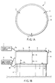
- a stage main body 2 can be a cylindrical body to match the shape of the semiconductor wafer.
- the stage main body 2 is not limited to a cylindrical body, but can employ any structure on which a target object can be placed appropriately.
- An upper electrode 3 is preferably arranged on an upper surface 2c of the stage main body 2.
- a semiconductor wafer W is arranged on the upper electrode 3.
- the upper electrode 3 preferably includes a fixing mechanism to fix the placed semiconductor wafer.
- the fixing mechanism can fix the semiconductor wafer by using a vacuum force.
- a potential control mechanism 7 can serve to apply a potential necessary for processing or testing the semiconductor wafer W to the upper electrode 3 through a cable 7a, or to remove an unnecessary potential.
- the upper electrode 3 can apply a potential to the semiconductor wafer W when, e.g., measuring a capacitance C of the semiconductor wafer W.
- the upper electrode 3 can have a plate structure made of a conductive metal, e.g., nickel or copper.
- the upper electrode 3 can also be formed by plating the upper surface of the stage main body 2 with the conductive metal.
- a lower electrode 4 can be arranged on a lower surface 2d of the stage main body 2.
- the lower electrode 4 can serve to set the potential of the lower portion of the stage main body 2 to be equal (guard potential) to that of a component in contact with or close to the stage main body 2.
- the lower electrode 4 can have a plate structure made of a conductive metal, e.g., nickel or copper.
- the lower electrode 4 can also be formed by plating the upper surface of the stage main body 2 with the conductive metal.
- the lower electrode 4 is preferably electrically connected to a guard potential setting mechanism 8 through a cable 8b.
- the lower electrode 4 sets the stage main body 2 at the guard potential. Then, the potential gradient between the stage main body 2 and the component disappears. Accordingly, the current can be prevented from flowing from the stage main body 2 to the component or vice versa.
- the stage main body 2 can be arranged on a base 6. Furthermore, a temperature control mechanism 5 can be arranged under the stage main body 2. The temperature control mechanism 5 heats or cools the stage main body 2.
- a side surface protection cover layer 10 is formed on the side surface of the stage main body 2.
- the side surface protection cover layer 10 isolates at least part of the side surface of the stage main body 2 from the ambient atmosphere of the main body 2. Consequently, an ionic material such as dust or soil is prevented from attaching to the side surface of the stage main body 2.
- the surface of the side surface protection cover layer 10 is preferably conductive.
- the conductive side surface protection cover layer 10 is connected to the guard potential setting mechanism 8 through a cable 8a.
- the side surface protection cover layer 10 can be maintained at the guard potential. Consequently, no unnecessary current flows out from the stage main body 2. No unnecessary current flows into the stage main body 2 from a peripheral component.
- the conductive side surface protection cover layer 10 and upper electrode 3 are preferably avoided from being electrically connected to each other.
- the position of the upper portion of the side surface protection cover layer 10 can be set below the upper surface of the stage main body 2 by a gap 10a.
- the constant gap 10a can be formed between the position of the upper portion of the side surface protection cover layer 10 and the upper surface of the stage main body 2.
- the length of the gap 10a can be set to at least 1 mm to 2 mm.
- the outer edge of the upper electrode 3 can be located inside the perimeter of a stage main body 2. More specifically, a gap 3a can be formed between the outer edge of the upper electrode 3 and the perimeter of the stage main body 2. The length of the gap 3a can be set to at least 1 mm to 2 mm.
- a conductive side surface protection cover layer 10 is to be set equal to that of the perimeter of a stage main body 2.
- an insulating layer 12 may be interposed between the side surface protection cover layer 10 and a side surface 2b of the stage main body 2. Then, electrical contact of the side surface protection cover layer 10 and side surface 2b can be prevented.
- the thickness of the insulating layer 12 is preferably at least 1 mm to 2 mm.
- the height of the insulating layer 12 may be larger, equal to, or smaller than that of the side surface protection cover layer 10. From the viewpoint of preventing electrical contact of the side surface protection cover layer 10 and side surface 2b, the height of the insulating layer 12 is preferably larger than that of the side surface protection cover layer 10.
- the conductive side surface protection cover layer 10 can have a plate-like conductive metal plate structure.
- the plate-structure side surface protection cover layer 10 can be fixed to the stage main body 2 with fixing means (e.g., screws) 11, as shown in FIG. 1B.
- fixing means e.g., screws
- the plate-structure side surface protection cover layer 10 can be fixed to the stage main body 2 with the screws at a plurality of portions (e.g., three portions).
- FIG. 1B shows hooks 2a and cutout catching portions 10b as an example of the dropping prevention mechanism.
- Each hook 2a projects from the side surface 2b of the stage main body 2.
- the cutout catching portions 10b are formed in the plate-like side surface protection cover layer 10.
- the cutout catching portions 10b of the plate-structure side surface protection cover layer 10 are engaged with the corresponding hooks 2a of the stage main body 2. With this engagement, the plate-structure side surface protection cover layer 10 can be attached to the side surface 2b of the stage main body 2 while it is prevented from dropping.
- the plate-structure side surface protection cover layer 10 can be made of a metal material (e.g., nickel or gold).
- the plate-structure side surface protection cover layer 10 can be made of a conductive plastic material.
- the outer surface of the plate-structure side surface protection cover layer 10 has a sufficiently large conductivity.
- the plate-like side surface protection cover layer 10 can have such an attaching structure that it can be detached from the stage main body 2 by using means such as screws. When the detachable attaching structure is employed, the maintenance operation of the plate-structure side surface protection cover layer 10 can be facilitated.
- a conductive side surface protection cover layer 10 can be formed by plating a side surface 2b of a stage main body 2.
- a gap 10a is preferably formed between an upper electrode 3 and the side surface protection cover layer 10 which is formed by plating.
- the gap 3a may be formed by decreasing the diameter of the upper electrode 3. Either gap can be set to 1 mm to 2 mm.
- the side surface protection cover layer can have a structure with a U-shaped section.
- the side surface protection cover layer is arranged on the side surface of the stage main body.
- an ionic material such as dust or dirt is prevented from attaching to the side surface of the stage main body.
- At least the surface of the side surface protection cover layer is rendered conductive, and the conductive surface is connected to the guard potential setting mechanism.
- a detachable attaching structure may be employed, which facilitates the maintenance operation for the plate-structure side surface protection cover layer.
- the side surface protection cover layer is formed by a plating process, or is made of a conductive plastic material, thus facilitating the manufacture.
- the conductive side surface protection cover layer and upper electrode are separate from each other, or an insulating layer is arranged between them. Then, flow of the current between the side surface protection cover layer and upper electrode can be prevented.
- a mechanism that prevents the side surface protection cover layer from dropping is employed.
- the side surface protection cover layer can be attached to the side surface of the stage main body stably.
Landscapes
- Container, Conveyance, Adherence, Positioning, Of Wafer (AREA)
- Testing Or Measuring Of Semiconductors Or The Like (AREA)
- Electron Beam Exposure (AREA)
- Exposure Of Semiconductors, Excluding Electron Or Ion Beam Exposure (AREA)
Applications Claiming Priority (2)
| Application Number | Priority Date | Filing Date | Title |
|---|---|---|---|
| JP2003373525A JP4142553B2 (ja) | 2003-10-31 | 2003-10-31 | 被処理体を載置するための載置台 |
| JP2003373525 | 2003-10-31 |
Publications (2)
| Publication Number | Publication Date |
|---|---|
| EP1528589A2 true EP1528589A2 (de) | 2005-05-04 |
| EP1528589A3 EP1528589A3 (de) | 2006-08-30 |
Family
ID=34420251
Family Applications (1)
| Application Number | Title | Priority Date | Filing Date |
|---|---|---|---|
| EP04024144A Withdrawn EP1528589A3 (de) | 2003-10-31 | 2004-10-09 | Halter zur Platzierung eines Zielobjektes |
Country Status (4)
| Country | Link |
|---|---|
| US (1) | US7183782B2 (de) |
| EP (1) | EP1528589A3 (de) |
| JP (1) | JP4142553B2 (de) |
| KR (1) | KR100709796B1 (de) |
Cited By (1)
| Publication number | Priority date | Publication date | Assignee | Title |
|---|---|---|---|---|
| US7183782B2 (en) * | 2003-10-31 | 2007-02-27 | Tokyo Electron Limited | Stage for placing target object |
Family Cites Families (10)
| Publication number | Priority date | Publication date | Assignee | Title |
|---|---|---|---|---|
| US5266889A (en) * | 1992-05-29 | 1993-11-30 | Cascade Microtech, Inc. | Wafer probe station with integrated environment control enclosure |
| US5345170A (en) * | 1992-06-11 | 1994-09-06 | Cascade Microtech, Inc. | Wafer probe station having integrated guarding, Kelvin connection and shielding systems |
| US6123864A (en) * | 1993-06-02 | 2000-09-26 | Applied Materials, Inc. | Etch chamber |
| JP3298810B2 (ja) * | 1997-07-09 | 2002-07-08 | 株式会社新川 | ダイボンディング装置 |
| JPH11233572A (ja) | 1998-02-16 | 1999-08-27 | Mitsubishi Electric Corp | 半導体試験装置 |
| JP2001176938A (ja) | 1999-12-20 | 2001-06-29 | Ibiden Co Ltd | ウエハプローバ |
| JP2001203257A (ja) | 2000-01-20 | 2001-07-27 | Sumitomo Electric Ind Ltd | 半導体製造装置用ウェハ保持体 |
| US6494955B1 (en) | 2000-02-15 | 2002-12-17 | Applied Materials, Inc. | Ceramic substrate support |
| KR20020095324A (ko) * | 2001-06-14 | 2002-12-26 | 삼성전자 주식회사 | 고주파 파워를 이용하는 반도체장치 제조설비 |
| JP4142553B2 (ja) * | 2003-10-31 | 2008-09-03 | 東京エレクトロン株式会社 | 被処理体を載置するための載置台 |
-
2003
- 2003-10-31 JP JP2003373525A patent/JP4142553B2/ja not_active Expired - Fee Related
-
2004
- 2004-10-01 US US10/954,546 patent/US7183782B2/en not_active Expired - Lifetime
- 2004-10-09 EP EP04024144A patent/EP1528589A3/de not_active Withdrawn
- 2004-10-28 KR KR1020040086710A patent/KR100709796B1/ko not_active Expired - Fee Related
Cited By (1)
| Publication number | Priority date | Publication date | Assignee | Title |
|---|---|---|---|---|
| US7183782B2 (en) * | 2003-10-31 | 2007-02-27 | Tokyo Electron Limited | Stage for placing target object |
Also Published As
| Publication number | Publication date |
|---|---|
| US20050093534A1 (en) | 2005-05-05 |
| EP1528589A3 (de) | 2006-08-30 |
| KR100709796B1 (ko) | 2007-04-23 |
| JP4142553B2 (ja) | 2008-09-03 |
| US7183782B2 (en) | 2007-02-27 |
| KR20050041925A (ko) | 2005-05-04 |
| JP2005136353A (ja) | 2005-05-26 |
Similar Documents
| Publication | Publication Date | Title |
|---|---|---|
| CN101175362B (zh) | 除电装置和除电方法 | |
| US6424141B1 (en) | Wafer probe station | |
| KR100889708B1 (ko) | 플라즈마 충전 전압의 실시간 측정 방법 | |
| KR101019878B1 (ko) | 프로브 장치, 프로브 방법 및 기억 매체 | |
| US11709199B2 (en) | Evaluation apparatus for semiconductor device | |
| JP2002040107A (ja) | プローブ駆動方法及びプローブ装置 | |
| JP5873741B2 (ja) | 半導体検査装置および半導体検査方法 | |
| JP2014521932A (ja) | 電子ビーム誘導プラズマプローブを用いた電子装置の電気検査 | |
| US12032012B1 (en) | Detection unit, semiconductor film layer inspection apparatus including the same, and semiconductor film layer inspection method using the same | |
| US7336471B2 (en) | Charge eliminating mechanism for stage and testing apparatus | |
| JP5280041B2 (ja) | プローブ支持台とプローブ支持台の使用の下で検査物質を検査する方法 | |
| EP0860704A2 (de) | Verfahren und Gerät zur Prüfung von integrierten Halbleiterschaltungen, und im Gerät eingebautes Prüfkontaktfeld | |
| US11391756B2 (en) | Probe module and probe | |
| US6781205B1 (en) | Electrostatic charge measurement on semiconductor wafers | |
| US4855673A (en) | Electron beam apparatus | |
| US7183782B2 (en) | Stage for placing target object | |
| US6563321B2 (en) | Method and apparatus for detecting line-shorts by potential and temperature distribution | |
| US20030139043A1 (en) | Apparatus and method for monitoring a plasma etch process | |
| EP4689675A1 (de) | Verfahren und messsondenvorrichtung zur messung eines parameters eines quantenchips | |
| JP2913344B2 (ja) | 半導体素子の検査装置及び検査方法。 | |
| US11977099B2 (en) | Method for manufacturing semiconductor device | |
| US10895587B2 (en) | Wafer probe station | |
| JP3783074B2 (ja) | ウエハ検査装置 | |
| JP2965174B2 (ja) | 半導体素子検査装置 | |
| US12000866B2 (en) | Detection unit, semiconductor film layer inspection apparatus including the same, and semiconductor film layer inspection method using the same |
Legal Events
| Date | Code | Title | Description |
|---|---|---|---|
| PUAI | Public reference made under article 153(3) epc to a published international application that has entered the european phase |
Free format text: ORIGINAL CODE: 0009012 |
|
| AK | Designated contracting states |
Kind code of ref document: A2 Designated state(s): AT BE BG CH CY CZ DE DK EE ES FI FR GB GR HU IE IT LI LU MC NL PL PT RO SE SI SK TR |
|
| AX | Request for extension of the european patent |
Extension state: AL HR LT LV MK |
|
| PUAL | Search report despatched |
Free format text: ORIGINAL CODE: 0009013 |
|
| AK | Designated contracting states |
Kind code of ref document: A3 Designated state(s): AT BE BG CH CY CZ DE DK EE ES FI FR GB GR HU IE IT LI LU MC NL PL PT RO SE SI SK TR |
|
| AX | Request for extension of the european patent |
Extension state: AL HR LT LV MK |
|
| 17P | Request for examination filed |
Effective date: 20070228 |
|
| AKX | Designation fees paid |
Designated state(s): DE FR GB IT NL |
|
| 17Q | First examination report despatched |
Effective date: 20070529 |
|
| GRAP | Despatch of communication of intention to grant a patent |
Free format text: ORIGINAL CODE: EPIDOSNIGR1 |
|
| STAA | Information on the status of an ep patent application or granted ep patent |
Free format text: STATUS: THE APPLICATION IS DEEMED TO BE WITHDRAWN |
|
| 18D | Application deemed to be withdrawn |
Effective date: 20100108 |