EP1526589A2 - Elektrolumineszente Anzeigevorrichtung - Google Patents
Elektrolumineszente Anzeigevorrichtung Download PDFInfo
- Publication number
- EP1526589A2 EP1526589A2 EP04024957A EP04024957A EP1526589A2 EP 1526589 A2 EP1526589 A2 EP 1526589A2 EP 04024957 A EP04024957 A EP 04024957A EP 04024957 A EP04024957 A EP 04024957A EP 1526589 A2 EP1526589 A2 EP 1526589A2
- Authority
- EP
- European Patent Office
- Prior art keywords
- emitting layer
- light
- packaging plate
- transparent substrate
- organic light
- Prior art date
- Legal status (The legal status is an assumption and is not a legal conclusion. Google has not performed a legal analysis and makes no representation as to the accuracy of the status listed.)
- Withdrawn
Links
Images




Classifications
-
- H—ELECTRICITY
- H05—ELECTRIC TECHNIQUES NOT OTHERWISE PROVIDED FOR
- H05B—ELECTRIC HEATING; ELECTRIC LIGHT SOURCES NOT OTHERWISE PROVIDED FOR; CIRCUIT ARRANGEMENTS FOR ELECTRIC LIGHT SOURCES, IN GENERAL
- H05B33/00—Electroluminescent light sources
- H05B33/02—Details
- H05B33/04—Sealing arrangements, e.g. against humidity
-
- H—ELECTRICITY
- H10—SEMICONDUCTOR DEVICES; ELECTRIC SOLID-STATE DEVICES NOT OTHERWISE PROVIDED FOR
- H10K—ORGANIC ELECTRIC SOLID-STATE DEVICES
- H10K59/00—Integrated devices, or assemblies of multiple devices, comprising at least one organic light-emitting element covered by group H10K50/00
- H10K59/80—Constructional details
- H10K59/87—Passivation; Containers; Encapsulations
- H10K59/871—Self-supporting sealing arrangements
- H10K59/8722—Peripheral sealing arrangements, e.g. adhesives, sealants
-
- H—ELECTRICITY
- H10—SEMICONDUCTOR DEVICES; ELECTRIC SOLID-STATE DEVICES NOT OTHERWISE PROVIDED FOR
- H10K—ORGANIC ELECTRIC SOLID-STATE DEVICES
- H10K50/00—Organic light-emitting devices
- H10K50/80—Constructional details
- H10K50/84—Passivation; Containers; Encapsulations
-
- H—ELECTRICITY
- H10—SEMICONDUCTOR DEVICES; ELECTRIC SOLID-STATE DEVICES NOT OTHERWISE PROVIDED FOR
- H10K—ORGANIC ELECTRIC SOLID-STATE DEVICES
- H10K50/00—Organic light-emitting devices
- H10K50/80—Constructional details
- H10K50/84—Passivation; Containers; Encapsulations
- H10K50/842—Containers
- H10K50/8426—Peripheral sealing arrangements, e.g. adhesives, sealants
-
- H—ELECTRICITY
- H10—SEMICONDUCTOR DEVICES; ELECTRIC SOLID-STATE DEVICES NOT OTHERWISE PROVIDED FOR
- H10K—ORGANIC ELECTRIC SOLID-STATE DEVICES
- H10K59/00—Integrated devices, or assemblies of multiple devices, comprising at least one organic light-emitting element covered by group H10K50/00
- H10K59/80—Constructional details
- H10K59/87—Passivation; Containers; Encapsulations
- H10K59/874—Passivation; Containers; Encapsulations including getter material or desiccant
Definitions
- the present invention relates to an electro luminescence display device, and more particularly to an electro luminescence display device that is adaptive for preventing the deterioration of an organic light-emitting layer by ultraviolet ray in a sealing process.
- Such flat panel display devices include a liquid crystal display (LCD), a field emission display (FED), a plasma display panel (PDP) and an electro-luminescence (EL) display, etc.
- LCD liquid crystal display
- FED field emission display
- PDP plasma display panel
- EL electro-luminescence
- the EL display in such display devices is a self-luminous device that makes a phosphorous material to emit light by a re-combination of electrons and holes.
- the EL display device is generally classified into an inorganic EL device using an inorganic compound as the phosphorous material and an organic EL using an organic compound as the phosphorus material.
- Such an EL display device has many advantages of a low voltage driving, a self-luminescence, a thin-thickness, a wide viewing angle, a fast response speed, a high contrast and so on such that it has been highlighted as a post-generation display device.
- the organic EL device is comprised of an electron injection layer, an electron transport layer, a light-emitting layer, a hole transport layer and a hole injection layer.
- an organic EL device when a predetermined voltage is applied between an anode and a cathode, electrons generated from the cathode move to the light-emitting layer through the electron injection layer and the electron transport layer, while holes generated from the anode move to the light-emitting layer through the hole injection layer and the hole transport layer. Accordingly, the electrons and the holes fed from the electron transport layer and the hole transport layer are re-combined to emit light.
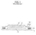
- an EL display device of prior art includes a transparent substrate 2, an organic light-emitting layer 18 formed on the transparent substrate 2, a packaging plate 24 to seal off the organic light-emitting layer 18 on the transparent substrate 2, and a sealant 22 to bond the packaging plate 24 with the transparent substrate 2.
- the organic light-emitting layer 18 includes an electron injection layer, an electron transport layer, a light-emitting layer, a hole transport layer and a hole injection layer that are deposited between an anode and a cathode (not shown).
- the organic light-emitting layer 18 if voltage is applied between a transparent electrode as the anode and a metal electrode as the cathode, the electrons generated from the cathode move to the light-emitting layer through the electron injection layer and the electron transport layer, and the holes generated from the anode move to the light emitting layer through the hole injection layer and the hole transport layer.
- the electrons and the holes supplied from the electron transport layer and the hole transport layer collide with each other to be recombined, thereby generating light.
- the light is emitted to the outside through the anode, the transparent electrode, to display a picture.
- the packaging plate 24 absorbs moisture and oxygen in the air, so a hygroscopic film 27 is stuck to the packaging plate 24 in order to protect the organic light-emitting layer 18 from the moisture and oxygen in the air.
- the packaging plate 24 includes a stepped part 30 having an incline plane 26 and a horizontal plane.
- the stepped part 30 provides an inner space, where the hygroscopic film 27 is stuck, in the central part of the packaging plate 24.
- the sealant 22 is spread between the transparent substrate 2 and the most outer stepped plane 28 of the packaging plate 24, and then it is hardened by ultraviolet ray to be illuminated, thereby bonding the packaging plate 24 with the transparent substrate 2. Due to this, the packaging plate 24 seals up the organic light-emitting layer 18 by being bonded with the transparent substrate 2 by the sealant 22 in a vacuum state.
- the electro luminescence display device of prior art bonds the transparent substrate 2 with the packaging plate 24 by a bonding device.
- the bonding device includes a large transparent substrate 2 where a plurality of organic light-emitting layers 18 are formed and which is fixed by a fixing means (not shown) ; a plurality of absorbers 50 to which a plurality of packaging plates 24 are absorbed, wherein the packaging plates 24 are bonded with the organic light-emitting layer 18; a sealant 22 spread at the edge of the transparent substrate 2 or the packaging plate 24; an UV illuminating device 60 to illuminate an ultraviolet ray 62 to the sealant 24; and a mask 64 to mask other area than the sealant 24 in order that the ultraviolet ray 62 is not illuminated onto each organic light-emitting layer 18.
- the absorbers 50 absorbs the packaging plate 24 supplied from the outside, using a pad 52.
- the absorber 50 has the packaging plate 24 absorbed on the pad 52 thereof and has the transparent substrate fixed thereto by a fixing means to align the organic light-emitting layer 18 formed on the transparent substrate 2 and the packaging plate 24.
- the ultraviolet ray 62 from the UV illuminating device 60 is illuminated onto the sealant 22 spread between the transparent substrate 2 and the packaging plate 24 for a designated time.
- the mask 64 allow the ultraviolet ray 62 illuminated from the UV illuminating device 60 to be illuminated only on the sealant 22 spread between the transparent substrate 2 and the packaging plate 24, and the ultraviolet ray 62 is intercepted at the remaining area.
- the sealant 22 is hardened by the ultraviolet ray 62 illuminated through the mask 64 to bond the transparent substrate 2 with the packaging plate 24.
- the ultraviolet ray 64 illuminated onto the sealant 22 through the mask 64 is dispersed by the incline plane 26 of the stepped plane 30 formed at the packaging plate 24 to generate a borrowed light 70. That is, the ultraviolet ray 64 is illuminated onto the sealant 22 to harden the sealant 22, and at the same time, is dispersed by the incline plane 26 of the stepped part 30 formed at the packaging plate 24 to generate the borrowed light 70.
- the borrowed light 70 repeats to be reflected over and over between the transparent substrate 2 and the incline plane 26 and the stepped plane 26 of the stepped part 30 formed at the packaging plate 24 to be illuminated onto the surrounding area of the organic light-emitting layer 18 and the EL display device. Accordingly, the borrowed light 70 is illuminated on to the organic light-emitting layer 18 to deteriorate the organic light-emitting layer 18, and in addition, is illuminated onto the surrounding area of the EL display device to change the characteristic of the driving devices inclusive of the transistor of the surrounding circuit of the EL display device.
- the EL display device of prior art has the edge of the organic light-emitting layer 18 deteriorated by the borrowed light 70 which are caused by the dispersion of ultraviolet ray 64 illuminated onto the sealant 22 upon the bonding process of the transparent substrate 2 and the packaging plate 24, and in addition, it has the characteristic of the driving devices of the surrounding circuit changed, thereby causing a brightness difference between the central part 80 of the EL display device and the other area 82, as shown in FIG. 4.
- an object of the present invention to provide an electro luminescence display device that is adaptive for preventing the deterioration of an organic light-emitting layer by ultraviolet ray in a sealing process.
- an electro luminescence display device includes a transparent substrate; an organic light-emitting layer formed on the transparent substrate; a packaging plate bonded with the transparent substrate by a sealant to cover the organic light-emitting layer; and a light-intercepting member to shut off that the ultraviolet ray illuminated onto the sealant upon bonding the transparent substrate with the packaging plate is reflected by the packaging plate to be illuminated onto the organic light-emitting layer.
- the light-intercepting member is a light-intercepting projected part which is projected toward the transparent substrate from the packaging plate.
- Thelight-intercepting projected partislocated between the sealant and the organic light-emitting layer is the light-intercepting projected partislocated between the sealant and the organic light-emitting layer.
- the light-intercepting projected part is projected from the packaging plate to be close to the organic light-emitting layer to the utmost.
- the electro luminescence display device wherein the light-intercepting projected part is formed to have a section of any one shape between a quadrangle and a triangle.
- the light-intercepting member is a plurality of light-intercepting projected parts that are projected toward the packaging plate from the transparent substrate.
- the light-intercepting projected parts are formed between the organic light-emitting layer and the end of the transparent substrate.
- Each of the light-intercepting projected parts is formed to have a section of any one shape between a quadrangle and a triangle.
- the light-intercepting member is an ultraviolet absorbing layer that is formed on the packaging plate to be opposite the transparent substrate and absorbs the ultraviolet ray.
- the ultraviolet absorbing layer is formed at the edge of the packaging plate so as to be opposite between the end of the transparent substrate and the edge of the organic light-emitting layer, and in addition, to overlap the edge of the organic light-emitting layer.
- FIG. 1 is a sectional diagram representing a general electro luminescence display device
- FIG. 2 is a sectional diagram representing a bonding process to bond a transparent substrate with a packaging plate, wherein the transparent substrate and the packaging plate are shown in FIG. 1;
- FIG. 3 is a sectional diagram of enlarged part A shown in FIG. 2;
- FIG. 4 is a view representing a brightness difference due to the deterioration of an organic light-emitting layer caused by an ultraviolet ray reflected by a packaging plate;
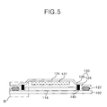
- FIG. 5 is a sectional diagram representing an electro luminescence display device according to a first embodiment of the present invention.
- FIG. 6 is a sectional diagram of enlarged part B shown in FIG. 5;
- FIG. 7 is a sectional diagram representing an electro luminescence display device according to a second embodiment of the present invention.
- FIG. 8 is a sectional diagram of enlarged part C shown in FIG. 7;
- FIG. 9 is a sectional diagram representing an electro luminescence display device according to a third embodiment of the present invention.
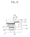
- FIG. 10 is a sectional diagram of enlarged part D shown in FIG. 9.
- an electro luminescence display device includes a transparent substrate 102; an organic light-emitting layer 118 formed on the transparent substrate 102; a packaging plate 124 to seal off the organic light-emitting layer 118 on the transparent substrate 102; a sealant 122 to bond the packaging plate 124 with the transparent substrate 102; and at least one light-intercepting projected part formed at the packaging plate 124 to prevent an ultraviolet ray illuminated onto the sealant 122 upon bonding the packaging plate 124 with the transparent substrate 102, from being illuminated onto the light-emitting layer 118.
- the organic light-emitting layer 118 includes an electron inj ection layer, an electron transport layer, a light-emitting layer, a hole transport layer and a hole injection layer that are deposited between an anode and a cathode (not shown).
- the organic light-emitting layer 118 if voltage is applied between a transparent electrode as the anode and a metal electrode as the cathode, the electrons generated from the cathode move to the light-emitting layer through the electron inj ection layer and the electron transport layer, and the holes generated from the anode move to the light emitting layer through the hole inj ection layer and the hole transport layer.
- the electrons and the holes supplied from the electron transport layer and the hole transport layer collide with each other to be recombined, thereby generating light.
- the light is emitted to the outside through the anode, the transparent electrode, to display a picture.
- the packaging plate 124 is bonded with the transparent substrate 102 by the sealant 122 to cover the organic light-emitting layer 118.
- the packaging plate 124 absorbs moisture and oxygen in the air, so a hygroscopic film 127 is stuck to the packaging plate 124 in order to protect the organic light-emitting layer 118 from the moisture and oxygen in the air.
- the packaging plate 124 includes a stepped part 130 having an incline plane 126 and a horizontal plane 128.
- the stepped part 130 provides an inner space, where the hygroscopic film 127 is stuck, in the central part of the packaging plate 124.
- the sealant 122 is spread between the transparent substrate 102 and the most outer stepped plane 128 of the packaging plate 124, and then it is hardened by ultraviolet ray to be illuminated, thereby bonding the packaging plate 124 with the transparent substrate 102. Due to this, the packaging plate 124 seals up the organic light-emitting layer 118 by being bonded with the transparent substrate 102 by the sealant 122 in a vacuum state.
- the at least one light-intercepting projected part 140 is projected toward the transparent substrate 102 to have a section of any one shape of a quadrangle and a triangle on the packaging plate 124 corresponding to and between the sealant 122 and the organic light-emitting layer 118. At this moment, the light-intercepting projected part 140 is projected to be close to the organic light-emitting layer 118 to the utmost, and in addition, to have a designated gap with the transparent substrate 102.
- the light-intercepting projected part 140 shut off that the ultraviolet ray illuminated onto the sealant 122 upon the bonding process of the transparent substrate 102 and the packaging plate 124 is dispersed by the incline plane 126 of the packaging plate 124 to deteriorate the organic light-emitting layer 118 and is illuminated onto the driving devices of the surrounding area of the EL display device.
- the electro luminescence display device illuminates the ultraviolet ray onto the sealant 122 spread at the edge of any one of the packaging plate 124, which protects the organic light-emitting layer 118 from the oxygen and moisture in the air, and the transparent substrate 102, where the organic light-emitting layer 118 is formed, to harden the sealant 122, thereby bonding the transparent 102 with the packaging plate 124.
- the light-intercepting projected part 140 as shown in FIG.
- the electro luminescence display device can prevent the deterioration of the organic light-emitting layer 118 and the characteristic change of the driving devices of the surrounding part of the EL display device caused by the borrowed light 170 that is generated by the packaging plate 124 upon the hardening of the sealant 122.
- an electro luminescence display device includes a transparent substrate 202; an organic light-emitting layer 218 formed on the transparent substrate 202; a packaging plate 224 to seal off the organic light-emitting layer 218 on the transparent substrate 202; a sealant 222 to bond the packaging plate 224 with the transparent substrate 202; and a plurality of light-intercepting projected part 240 projected toward the packaging plate 224 from the transparent substrate 202 to prevent a borrowed light caused by the dispersion of an ultraviolet ray illuminated onto the sealant 222 upon bonding the packaging plate 224 with the transparent substrate 202, from being illuminated onto the light-emitting layer 218.
- the organic light-emitting layer 218 includes an electron injectionlayer, an electron transport layer, a light-emitting layer, a hole transport layer and a hole injection layer that are deposited between an anode and a cathode (not shown).
- the electrons and the holes supplied from the electron transport layer and the hole transport layer collide with each other to be recombined, thereby generating light.
- the light is emitted to the outside through the anode, the transparent electrode, to display a picture.
- the packaging plate 224 is bonded with the transparent substrate 202 by the sealant 222 to cover the organic light-emitting layer 218.
- the packaging plate 224 absorbs moisture and oxygen in the air, so a hygroscopic film 227 is stuck to the packaging plate 224 in order to protect the organic light-emitting layer 218 from the moisture and oxygen in the air.
- the packaging plate 224 includes a stepped part 230 having an incline plane 226 and a horizontal plane 228.
- the stepped part 230 provides an inner space, where the hygroscopic film 227 is stuck, in the central part of the packaging plate 224.
- the sealant 222 is spread between the transparent substrate 202 and the most outer stepped plane 228 of the packaging plate 224, and then it is hardened by ultraviolet ray to be illuminated, thereby bonding the packaging plate 224 with the transparent substrate 202.
- the packaging plate 224 seals up the organic light-emitting layer 218 by being bonded with the transparent substrate 202 by the sealant 222 in a vacuum state.
- the light-intercepting projected parts 240 are projected toward a transparent substrate 202 to have a section of any one shape of a quadrangle and a triangle at the edge of the transparent substrate 202.
- the light-intercepting projected part 240 is formed between the organic light-emitting layer 218 and the end of the transparent substrate 202, and the sealant 222 is spread on part of the light-intercepting projected part 240.
- the light-intercepting projected parts 240 shut off that the ultraviolet ray illuminated onto the sealant 222 upon the bonding process of the transparent substrate 202 and the packaging plate 224 is dispersed by the incline plane 226 of the packaging plate 224 to deteriorate the organic light-emitting layer 218 and is illuminated onto the driving devices of the surrounding area of the EL display device.
- the electro luminescence display device illuminates the ultraviolet ray onto the sealant 222 spread at the edge of any one of the packaging plate 224, which protects the organic light-emitting layer 218 from the oxygen and moisture in the air, and the transparent substrate 202, where the organic light-emitting layer 218 is formed, to harden the sealant 222, thereby bonding the transparent 202 with the packaging plate 224.
- the light-intercepting projected parts 240 as shown in FIG.
- the light-intercepting projected part 240 is projected on the transparent substrate 202 to be close to the packaging plate to the utmost in order to shut off that the borrowed light 270 progresses to the organic light-emitting layer 218 by the packaging plate 224.
- the electro luminescence display device can prevent the deterioration of the organic light-emitting layer 218 and the characteristic change of the driving devices of the surrounding part of the EL display device caused by the borrowed light 270 that is generated by the packaging plate 224 upon the hardening of the sealant 222.
- an electro luminescence display device includes a transparent substrate 302; an organic light-emitting layer 318 formed on the transparent substrate 302; a packaging plate 324 to seal off the organic light-emitting layer 318 on the transparent substrate 302; a sealant 322 to bond the packaging plate 324 with the transparent substrate 302; and an ultraviolet ray absorbing layer 340 formed at the packaging plate 324 to prevent an ultraviolet ray illuminated onto the sealant 322 upon bonding the packaging plate 324 with the transparent substrate 302, from being illuminated onto the light-emitting layer 318.
- the organic light-emitting layer 318 includes an electron injection layer, an electron transport layer, a light-emitting layer, a hole transport layer and a hole injection layer that are deposited between an anode and a cathode (not shown).
- the organic light-emitting layer 318 if voltage is applied between a transparent electrode as the anode and a metal electrode as the cathode, the electrons generated from the cathode move to the light-emitting layer through the electron inj ection layer and the electron transport layer, and the holes generated from the anode move to the light emitting layer through the hole injection layer and the hole transport layer.
- the electrons and the holes supplied from the electron transport layer and the hole transport layer collide with each other to be recombined, thereby generating light.
- the light is emitted to the outside through the anode, the transparent electrode, to display a picture.
- the packaging plate 324 is bonded with the transparent substrate 302 by the sealant 322 to cover the organic light-emitting layer 318.
- the packaging plate 324 absorbs moisture and oxygen in the air, so a hygroscopic film 327 is stuck to the packaging plate 324 in order to protect the organic light-emitting layer 318 from the moisture and oxygen in the air.
- the packaging plate 324 includes a stepped part 330 having an incline plane 326 and a horizontal plane 328.
- the stepped part 330 provides an inner space, where the hygroscopic film 327 is stuck, in the central part of the packaging plate 324.
- the sealant 322 is spread between the transparent substrate 302 and the most outer stepped plane 328 of the packaging plate 324, and then it is hardened by ultraviolet ray to be illuminated, thereby bonding the packaging plate 324 with the transparent substrate 302.
- the packaging plate 324 seals up the organic light-emitting layer 318 by being bonded with the transparent substrate 302 by the sealant 322 in a vacuum state.
- the ultraviolet absorbing layer 340 is formed at the horizontal plane 328 ad the incline plane 326 of the edge of the packaging plate 324 that are corresponding to the edge of the transparent substrate 302.
- the ultraviolet absorbing layer 340 is formed at the rear surface of the packaging plate 324 to be opposite between the end of the transparent substrate 302 and the end of the organic light-emitting layer 318. At this moment, the ultraviolet absorbing layer 340 is formed to overlap the edge area of the organic light-emitting layer 318.
- the ultraviolet absorbing layer 340 shut off that the ultraviolet ray illuminated onto the sealant 322 upon the bonding process of the transparent substrate 302 and the packaging plate 324 is dispersed by the incline plane 326 of the packaging plate 324 to deteriorate the organic light-emitting layer 318 and is illuminated onto the driving devices of the surrounding area of the EL display device.
- the electro luminescence display device illuminates the ultraviolet ray onto the sealant 322 spread at the edge of any one of the packaging plate 324, which protects the organic light-emitting layer 318 from the oxygen and moisture in the air, and the transparent substrate 302, where the organic light-emitting layer 318 is formed, to harden the sealant 322, thereby bonding the transparent 302 with the packaging plate 324.
- the ultraviolet absorbing layer 340 as shown in FIG. 10, when the ultraviolet ray 362 is illuminated onto the sealant 322, absorbs the ultraviolet ray 362 that is reflected toward the organic light-emitting layer 318 by the incline plane 326 and the horizontal plane 328 of the packaging plate 324.
- the ultraviolet absorbing layer 340 reduces the reflection efficiency of the illuminated ultraviolet ray 362 to shut off that the borrowed light 370 generated by being dispersed by the incline plane 326 and the horizontal plane 328 of the packaging plate 324 is reflected toward the organic light-emitting layer 318. Accordingly, the electro luminescence display device according to the third embodiment of the present invention can prevent the deterioration of the organic light-emitting layer 318 and the characteristic change of the driving devices of the surrounding part of the EL display device caused by the borrowed light 370 that is generated by the packaging plate 324 upon the hardening of the sealant 322.
- the electro luminescence display device includes the light-intercepting projected part which is projected toward the transparent substrate from the edge of the packaging plate. Accordingly, the present invention intercepts the ultraviolet ray which is illustrated onto the sealant upon bonding the transparent substrate with the packaging plate and reflected by the packaging plate to be illustrated onto the organic light-emitting layer, thereby preventing the deterioration of the organic light-emitting layer and the characteristic change of the driving devices of the surrounding part of the EL display device.
- the electro luminescence display device includes a plurality of light-intercepting projected parts which are proj ected toward the packaging plate from the edge of the transparent substrate. Accordingly, the present invention shuts off the ultraviolet ray, which is illuminated onto the sealant upon bonding the transparent substrate with the packaging plate and reflected by the packaging plate to be illuminated onto the organic light-emitting layer, by use of the plurality of light-intercepting proj ected parts, thereby preventing the deterioration of the organic light-emitting layer and the characteristic change of the driving devices of the surrounding area of the EL display device.
- the electro luminescence display device includes the ultraviolet absorbing layer that is formed at the edge of the packaging plate. Accordingly, the present invention absorbs the ultraviolet ray, which is illuminated onto the sealant upon bonding the transparent substrate with the packaging plate and reflected by the packaging plate to be illuminated onto the organic light-emitting layer, by use of the ultraviolet absorbing layer, thereby preventing the deterioration of the organic light-emitting layer and the characteristic change of the driving devices of the surrounding area of the EL display device.
Landscapes
- Physics & Mathematics (AREA)
- Optics & Photonics (AREA)
- Electroluminescent Light Sources (AREA)
Applications Claiming Priority (2)
| Application Number | Priority Date | Filing Date | Title |
|---|---|---|---|
| KR1020030073310A KR100551121B1 (ko) | 2003-10-21 | 2003-10-21 | 일렉트로 루미네센스 표시장치 |
| KR2003073310 | 2003-10-21 |
Publications (2)
| Publication Number | Publication Date |
|---|---|
| EP1526589A2 true EP1526589A2 (de) | 2005-04-27 |
| EP1526589A3 EP1526589A3 (de) | 2006-07-26 |
Family
ID=34386784
Family Applications (1)
| Application Number | Title | Priority Date | Filing Date |
|---|---|---|---|
| EP04024957A Withdrawn EP1526589A3 (de) | 2003-10-21 | 2004-10-20 | Elektrolumineszente Anzeigevorrichtung |
Country Status (3)
| Country | Link |
|---|---|
| US (1) | US7189990B2 (de) |
| EP (1) | EP1526589A3 (de) |
| KR (1) | KR100551121B1 (de) |
Families Citing this family (12)
| Publication number | Priority date | Publication date | Assignee | Title |
|---|---|---|---|---|
| US8405193B2 (en) * | 2004-04-02 | 2013-03-26 | General Electric Company | Organic electronic packages having hermetically sealed edges and methods of manufacturing such packages |
| KR100892413B1 (ko) * | 2007-10-12 | 2009-04-10 | 전자부품연구원 | 유기 발광 다이오드 조명 장치 및 그의 제조 방법 |
| KR101023129B1 (ko) * | 2008-07-25 | 2011-03-18 | 삼성모바일디스플레이주식회사 | 유기 발광 표시 장치 및 그 제조 방법 |
| KR101146985B1 (ko) * | 2010-03-11 | 2012-05-23 | 삼성모바일디스플레이주식회사 | 표시 장치 및 이의 제조 방법 |
| TWI574442B (zh) * | 2014-04-10 | 2017-03-11 | 友達光電股份有限公司 | 顯示面板 |
| KR102404720B1 (ko) * | 2015-03-03 | 2022-06-02 | 삼성디스플레이 주식회사 | 표시 장치 |
| CN105470410B (zh) * | 2016-02-24 | 2018-05-29 | 上海天马有机发光显示技术有限公司 | 一种显示面板及其封装方法 |
| CN106935731B (zh) | 2017-05-15 | 2020-03-06 | 京东方科技集团股份有限公司 | 有机电致发光显示器件和显示装置 |
| KR102430794B1 (ko) * | 2017-11-30 | 2022-08-08 | 엘지디스플레이 주식회사 | 디스플레이 장치 |
| CN109950414A (zh) * | 2019-01-31 | 2019-06-28 | 昆山国显光电有限公司 | 一种显示面板及显示设备 |
| CN110571347B (zh) * | 2019-08-09 | 2021-04-02 | 武汉华星光电半导体显示技术有限公司 | 一种显示面板及其制备方法 |
| CN114709348B (zh) * | 2022-03-31 | 2026-02-10 | 武汉天马微电子有限公司 | 显示模组和显示装置 |
Citations (6)
| Publication number | Priority date | Publication date | Assignee | Title |
|---|---|---|---|---|
| EP0884930A1 (de) | 1996-02-26 | 1998-12-16 | Idemitsu Kosan Company Limited | Organisches elektrolumineszentes element und verfahren zur herstellung desselben |
| JP2000150145A (ja) | 1998-11-02 | 2000-05-30 | Toyota Motor Corp | El素子の密封方法 |
| JP2001126868A (ja) | 1999-10-28 | 2001-05-11 | Idemitsu Kosan Co Ltd | 有機エレクトロルミネッセンス素子の製造方法 |
| US20020018911A1 (en) | 1999-05-11 | 2002-02-14 | Mark T. Bernius | Electroluminescent or photocell device having protective packaging |
| US20030042852A1 (en) | 2001-09-05 | 2003-03-06 | Hwa-Fu Chen | Encapsulation structure, method, and apparatus for organic light-emitting diodes |
| US20030062518A1 (en) | 1999-12-17 | 2003-04-03 | Mark Auch | Method for encapsulation of electronic devices |
Family Cites Families (8)
| Publication number | Priority date | Publication date | Assignee | Title |
|---|---|---|---|---|
| US3997892A (en) | 1973-07-27 | 1976-12-14 | Trw Inc. | Digital to analog converter with improved companding |
| US5482896A (en) * | 1993-11-18 | 1996-01-09 | Eastman Kodak Company | Light emitting device comprising an organic LED array on an ultra thin substrate and process for forming same |
| US6268071B1 (en) * | 1997-08-29 | 2001-07-31 | Tdk Corporation | Organic electroluminescent device |
| US6225931B1 (en) | 1999-08-30 | 2001-05-01 | Industrial Technology Research Institute | D/A converter with a gamma correction circuit |
| JP2002156938A (ja) | 2000-11-21 | 2002-05-31 | Canon Inc | 画像表示装置およびその駆動方法 |
| US6537688B2 (en) * | 2000-12-01 | 2003-03-25 | Universal Display Corporation | Adhesive sealed organic optoelectronic structures |
| JP3884351B2 (ja) | 2002-08-26 | 2007-02-21 | 株式会社 日立ディスプレイズ | 画像表示装置およびその製造方法 |
| US6982470B2 (en) * | 2002-11-27 | 2006-01-03 | Seiko Epson Corporation | Semiconductor device, method of manufacturing the same, cover for semiconductor device, and electronic equipment |
-
2003
- 2003-10-21 KR KR1020030073310A patent/KR100551121B1/ko not_active Expired - Fee Related
-
2004
- 2004-10-20 EP EP04024957A patent/EP1526589A3/de not_active Withdrawn
- 2004-10-20 US US10/968,186 patent/US7189990B2/en not_active Expired - Lifetime
Patent Citations (6)
| Publication number | Priority date | Publication date | Assignee | Title |
|---|---|---|---|---|
| EP0884930A1 (de) | 1996-02-26 | 1998-12-16 | Idemitsu Kosan Company Limited | Organisches elektrolumineszentes element und verfahren zur herstellung desselben |
| JP2000150145A (ja) | 1998-11-02 | 2000-05-30 | Toyota Motor Corp | El素子の密封方法 |
| US20020018911A1 (en) | 1999-05-11 | 2002-02-14 | Mark T. Bernius | Electroluminescent or photocell device having protective packaging |
| JP2001126868A (ja) | 1999-10-28 | 2001-05-11 | Idemitsu Kosan Co Ltd | 有機エレクトロルミネッセンス素子の製造方法 |
| US20030062518A1 (en) | 1999-12-17 | 2003-04-03 | Mark Auch | Method for encapsulation of electronic devices |
| US20030042852A1 (en) | 2001-09-05 | 2003-03-06 | Hwa-Fu Chen | Encapsulation structure, method, and apparatus for organic light-emitting diodes |
Also Published As
| Publication number | Publication date |
|---|---|
| US7189990B2 (en) | 2007-03-13 |
| US20050116221A1 (en) | 2005-06-02 |
| EP1526589A3 (de) | 2006-07-26 |
| KR20050038101A (ko) | 2005-04-27 |
| KR100551121B1 (ko) | 2006-02-13 |
Similar Documents
| Publication | Publication Date | Title |
|---|---|---|
| US6861801B2 (en) | Organic electroluminescence display device having sealing structure and method of fabricating the same | |
| US7189990B2 (en) | Electro luminescence display device | |
| US6784612B2 (en) | Organic EL display device and method of encapsulating the same | |
| US20080203909A1 (en) | Organic electroluminescence display device | |
| KR100667358B1 (ko) | 일렉트로-루미네센스 표시장치 | |
| CN104253239B (zh) | 有机发光二极管显示装置 | |
| US20070194308A1 (en) | Organic light emitting display capable of showing images on double sides thereof | |
| US7486007B2 (en) | Flat panel display device | |
| KR20030044659A (ko) | 유기 el 소자 | |
| KR102891662B1 (ko) | Oled 모듈 및 그를 구비한 디스플레이 장치 | |
| KR20150015139A (ko) | 유기 발광 디스플레이 장치 및 그의 제조방법 | |
| US10100985B2 (en) | Organic light-emitting device for lighting | |
| JP2004087496A (ja) | 有機電界発光表示装置 | |
| KR101307547B1 (ko) | 유기 발광 다이오드 표시장치 | |
| KR100592392B1 (ko) | 유기 전계발광표시소자 및 그 제조방법 | |
| KR20060129899A (ko) | 평판 표시소자용 마스크 | |
| US20060289857A1 (en) | Organic light emitting display capable of showing images on double sides thereof | |
| KR20060077466A (ko) | 유기발광소자의 봉지 구조 및 봉지 방법 | |
| KR100712122B1 (ko) | 평판표시장치 | |
| KR101001994B1 (ko) | 유기 전계발광소자 및 그 제조방법 | |
| KR100705340B1 (ko) | 일렉트로 루미네센스 표시장치 | |
| KR101193177B1 (ko) | 평판 표시 장치 | |
| KR20050007902A (ko) | 유기 전계 발광표시장치 | |
| KR100621862B1 (ko) | 일렉트로 루미네센스 표시패널의 패키징 케이스 | |
| KR100413434B1 (ko) | 유기 이엘(el) 소자의 밀봉구조 |
Legal Events
| Date | Code | Title | Description |
|---|---|---|---|
| PUAI | Public reference made under article 153(3) epc to a published international application that has entered the european phase |
Free format text: ORIGINAL CODE: 0009012 |
|
| 17P | Request for examination filed |
Effective date: 20041021 |
|
| AK | Designated contracting states |
Kind code of ref document: A2 Designated state(s): AT BE BG CH CY CZ DE DK EE ES FI FR GB GR HU IE IT LI LU MC NL PL PT RO SE SI SK TR |
|
| AX | Request for extension of the european patent |
Extension state: AL HR LT LV MK |
|
| PUAL | Search report despatched |
Free format text: ORIGINAL CODE: 0009013 |
|
| AK | Designated contracting states |
Kind code of ref document: A3 Designated state(s): AT BE BG CH CY CZ DE DK EE ES FI FR GB GR HU IE IT LI LU MC NL PL PT RO SE SI SK TR |
|
| AX | Request for extension of the european patent |
Extension state: AL HR LT LV MK |
|
| 17Q | First examination report despatched |
Effective date: 20060907 |
|
| AKX | Designation fees paid |
Designated state(s): AT BE BG CH CY CZ DE DK EE ES FI FR GB GR HU IE IT LI LU MC NL PL PT RO SE SI SK TR |
|
| GRAP | Despatch of communication of intention to grant a patent |
Free format text: ORIGINAL CODE: EPIDOSNIGR1 |
|
| RIC1 | Information provided on ipc code assigned before grant |
Ipc: H01L 51/52 20060101AFI20140331BHEP |
|
| INTG | Intention to grant announced |
Effective date: 20140416 |
|
| STAA | Information on the status of an ep patent application or granted ep patent |
Free format text: STATUS: THE APPLICATION IS DEEMED TO BE WITHDRAWN |
|
| 18D | Application deemed to be withdrawn |
Effective date: 20140827 |
|
| REG | Reference to a national code |
Ref country code: DE Ref legal event code: R079 Free format text: PREVIOUS MAIN CLASS: H01L0051200000 Ipc: H01L0051050000 |
|
| REG | Reference to a national code |
Ref country code: DE Ref legal event code: R079 Free format text: PREVIOUS MAIN CLASS: H01L0051200000 Ipc: H01L0051050000 Effective date: 20150225 |