EP1526546A1 - Relationaler inhaltsadressierbarer Speicher - Google Patents
Relationaler inhaltsadressierbarer Speicher Download PDFInfo
- Publication number
- EP1526546A1 EP1526546A1 EP04256444A EP04256444A EP1526546A1 EP 1526546 A1 EP1526546 A1 EP 1526546A1 EP 04256444 A EP04256444 A EP 04256444A EP 04256444 A EP04256444 A EP 04256444A EP 1526546 A1 EP1526546 A1 EP 1526546A1
- Authority
- EP
- European Patent Office
- Prior art keywords
- mcam
- magnitude
- signal
- cell
- comparison
- Prior art date
- Legal status (The legal status is an assumption and is not a legal conclusion. Google has not performed a legal analysis and makes no representation as to the accuracy of the status listed.)
- Granted
Links
Images



Classifications
-
- G—PHYSICS
- G06—COMPUTING OR CALCULATING; COUNTING
- G06F—ELECTRIC DIGITAL DATA PROCESSING
- G06F7/00—Methods or arrangements for processing data by operating upon the order or content of the data handled
- G06F7/02—Comparing digital values
- G06F7/026—Magnitude comparison, i.e. determining the relative order of operands based on their numerical value, e.g. window comparator
-
- G—PHYSICS
- G11—INFORMATION STORAGE
- G11C—STATIC STORES
- G11C15/00—Digital stores in which information comprising one or more characteristic parts is written into the store and in which information is read-out by searching for one or more of these characteristic parts, i.e. associative or content-addressed stores
Definitions
- This invention relates generally to the field of computer memory. More particularly, this invention relates to a content addressable memory (CAM) for determining if a comparison value is greater than or less than a stored value.
- CAM content addressable memory
- RAM arrays have a number of memory cells arranged in rows and columns and include addressing circuitry that addresses a selected row of memory cells.
- the address of a memory cell corresponds to a physical location of the cell in the memory array.
- each memory location In order to determine if a particular data value is stored on memory, each memory location must be searched. In the course of the search, an address is supplied to the memory and the memory returns the data value stored at that address.
- a content addressable memory In contrast, in a content addressable memory (CAM), data values are addressed by their content rather than by a physical memory location. In order to determine if a particular data value is stored in the memory, the data value (the comparison value) is supplied to the memory and the rows of the CAM assert or de-assert an associated match signal depending on whether or not the comparison value matches one or more data values stored in the CAM cell row. Optionally, additional data associated with the matched value can be output.
- a CAM may be preloaded with a pre-defined data set including data to be compared (keys) and, optionally, data to be output when a match is found.
- the address where the match is found can be used as an index to a secondary memory or other device.
- CAM devices are used for address look-up functions in Internet data routing. The Internet address is used as the comparison value or key, and is associated with routing information.
- image data may be stored using pixel color as the key, thereby allowing pixel data stored in memory to be searched for pixels of a particular color.
- Each memory cell of a binary CAM device stores the values 0 and 1, while ternary devices store the values 1, 0 and 'don't care'.
- the 'don't care' value will match with either a one or a zero. In either case, the output match value is a binary 0 or 1.
- Ternary CAM devices provide the ability to match variable length words to stored values. A bit in the word can be masked globally or individually.
- New requirements in the field of networking are not satisfied by a simple match of a stored word and comparison word. For example, it may be necessary to compare ranges of values. Using present memory devices, multiple comparisons must be made to determine matches within a range.
- the present invention relates generally to content addressable memory devices. Objects and features of the invention will become apparent to those of ordinary skill in the art upon consideration of the following detailed description of the invention.
- a magnitude content addressable memory (Magnitude CAM or MCAM) is provided that determines whether a comparison word is 'greater than' or 'less than' a stored value. As a by-product, a perfect match may also be determined. The width of the stored and comparison words is limited only by physical area and the speed requirements of the comparison.
- FIG. 1 is a diagrammatic representation of a magnitude content addressable memory (Magnitude CAM or MCAM) in accordance with the present invention.
- the cell determines whether a comparison word is 'greater than' or 'less than' a stored value. As a by-product, a perfect match may also be determined.
- the width of the stored and comparison words is limited only by physical area and the speed requirements of the comparison.
- the cell may require more transistors than a standard ternary CAM (TCAM) cell and consequently may by larger. However, the increase in cell area is compensated by the increased capability of the magnitude CAM.
- FIG. 1 shows the basic circuitry for a single MCAM cell.
- the first stage contains two memory cells, 102 and 104.
- FIG. 1 shows a ternary version of the cell having two memory cells 102 and 104. However, if individual bit masking is not required the second memory cell, 104, may be omitted, thereby reducing the number of transistors required.
- the inputs for these cells are typical for SRAM cells, having a word line running horizontally across each row and bit lines running vertically from row to row of the MCAM.
- the data memory cell 102 is used to store a data value and is controlled by word line VWL.
- Data to be written to the cell is carried in bit lines BLT and BLC, which denote the true bit value (T) and its complement (C).
- the mask memory cell 104 is used to store a mask value and is controlled by word line MWL. Data to be written to the cell is carried in the same bit lines BLT and BLC, which denote the true bit value (T) and complement (C) of the mask.
- An SRAM cell has two internal nodes, corresponding to the true and complementary values of the stored datum.
- the internal nodes values of the data memory cell 102 are output on lines DATAT and DATAC, which denote the true and complementary values, respectively.
- the internal node values of the mask memory cell 104 are output on lines MASKT and MASKC, denoting the true and complementary values, respectively.
- the DATAT, DATAC and MASKT lines are used by the next stage of the cell.
- Other types of memory cells may provide only the true values as outputs, in which case the DATAC signal may be generated by passing the DATAT signal through an inverter.
- the DATAT, DATAC and MASKT lines are passed to a controlled magnitude comparator 106.
- the magnitude comparator also receives signals denoting the true and complementary values of the comparison bit (COMPT and COMPC respectively). If the MASKT signal is not asserted (i.e. it is a logical 0) the magnitude comparator compares the DATAT and COMPT values to determine which is larger.
- the operation of the controlled magnitude comparator is discussed in more detail below with reference to FIG. 2 . If the mask memory cell is omitted, the magnitude comparator is not controlled by the mask signal and the magnitude comparator compares the COMPT and DATAT signals to determine which is larger.
- FIG. 2 shows an exemplary controlled magnitude comparator 106.
- the first stage 202 of the comparator is a controlled XOR gate. The function of this gate is to determine if the two sets of inputs are the same.
- the circuit shown is a CMOS gate, but could be any gate that performs the XOR function.
- the inputs are the compare lines COMPT and COMPC, which run vertically from row to row of the MCAM cells and the internal nodes (DATAT and DATAC) of the data memory cell.
- the comparison value COMPT and the stored data value DATAT are passed to AND gate 206, while the complementary signals COMPC and the stored data value DATAC are passed to AND gate 208.
- the outputs from AND gate 206 and AND gate 208 are passed to NOR gate 212.
- the output of the gate is forced into a low state, which is effectively a bypass state for the carry signals.
- the function of the first stage 202 is to produce a match signal and its complement.
- the stage could be implemented using other combinations of logic elements. For example, and XNOR gate followed by a NOR gate could be used.
- the next stage, 204 in FIG. 2 is a series of CMOS transmission gates and an inverter 212 that form a magnitude comparator.
- the gates 214 and 218 perform the 'greater than' function while the gates 216 and 220 perform the 'less than' function.
- the output from the NOR gate 210 is supplied to one side of each gate while its complement, the output from the inverter 212 is supplied to the other side of the gate.
- Other types of signal gates could be used, however the use of transmission gates that employ both P-channel and N-channel transistors avoids signal degradation. This is beneficial since the MCAM cells may be cascaded in series in a row of the MCAM device. This form of magnitude comparator is known in the art.
- Previous carry signals CRYGP and CRYLP are passed to the magnitude comparator from the preceding MCAM cell in the row.
- the carry signals also called magnitude signals, denote whether the comparison value is greater than the data value and whether the comparison value is less than the data value. Together, the magnitude signals also indicate if the comparison and data values are equal.
- the inputs to the first cell of a row may be grounded to represent a logical zero.
- the previous carry signals denote the results of comparing data bits having a lower significance. Depending upon the result of the XNOR gate, either the previous carry signals or the new data are passed on as the new carry or magnitude signals CRYG and CRYL.
- the previous carry signals CRYGP and CRYLP are passed because the comparison has not changed and still determined by the lower bits.
- FIG. 3 is a diagrammatic representation of a row of four ternary MCAM cells 100 in accordance with certain aspects of the present invention.
- any number of MCAM cells may be configured a row, allowing comparison of words of various lengths.
- the left most cell stores the least significant bit of the data word.
- the carry outputs CRYG and CRYL of each MCAM cell are connected to the previous carry inputs (CRYGP and CRYLP) of the subsequent MCAM cell.
- the CRYGP and CRYLP inputs of the leftmost cell are grounded at ground connection 326.
- Word input lines 310 and 312 are connected to each MCAM cell.
- the signal MWL is asserted on line 310 to enable data to be written to the mask memory of each cell, while the signal VWL is asserted on line 312 to enable data to be written to the data memory of each cell.
- the data itself is supplied on bit line inputs 314 that may be arrayed in typical SRAM fashion.
- the signal BLT ⁇ 0:3> specifies the four bits to be written, with one bit being written to each MCAM cell. The least significant bit is written to the leftmost cell.
- An optional additional bit line 316 carries complementary data BLC ⁇ 0:3> to be written to the memory cells. This line is required for example when SRAM cells are used since they have two internal nodes.
- the comparison inputs 306 and 308 are also arrayed.
- the signal COMPT ⁇ 0:3> comprises four bits, each of which is supplied to one of the four MCAM cells.
- complementary comparison values COMPC ⁇ 0:3> are also supplied to the MCAM cells.
- the magnitude or carry outputs 322 (CRYG) and 324 (CRYL) from the right most MCAM cell (which compares the most significant bits of the data value and the comparison value) are passed to a second stage comparator 302, along with outputs 318 (CRYGP) and 320 (CRYLP) from previous stages.
- the outputs from the second stage comparator 302, denoted as CRYGN and CRYLN are passed to the next stage. The operation of the second stage comparator 302 will be discussed below in reference to FIG. 4 .
- the input CRYP is taken to denote CRYGP when considering CRYG (since CRYG does not depend upon CRYLP) and taken to denote CRYLP when considering CRYL.
- CRYGP when considering CRYG
- CRYLP when considering CRYL.
- CRYGP and CRYLP are initialized at cell 1 to zero.
- the computation proceeds as follows:
- a simple NOR gate having CRYG and CRYL as inputs would produce a match or equality signal.
- the MCAM device of the present invention may be implemented using positive or negative logic.
- the number of MCAM cells may be chosen to produce any word length. When long word lengths are required, it may be necessary to use inverter buffers or other devices to boost the CRYG and CRYL signals. In a test configuration of four MCAM cells the signal degradation was not severe enough to require buffering to boost the signals. If more cells are added then using inverter buffers or other booster buffers between CRYG and CRYGP will improve performance. The same is true for CRYL and CRYLP.
- the buffers may be used between every cell, every other cell or wherever needed to achieve a required performance.
- the subsequent cell When an inverter buffer is used between cells, the subsequent cell should use negative logic inputs relative to the preceding cell to control the transfer gates (204 in FIG. 2 ). For example, if the transfer gates 204 of the cell prior to the inverter used the signals COMPT and DATAT the subsequent gate should use the signals COMPC and DATAC.
- FIG. 3 A second stage comparator 302 coupled to a group of MCAM cells is shown in FIG. 3 .
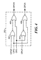
- An exemplary embodiment of a second stage comparator 302 is shown in FIG. 4 .
- the second stage comparator 302 comprises a group of NOR gates which tie together the outputs of MCAM groups.
- the output CRYG from the current MCAM group is passed to NOR gate 402 together with the carry signal CRYGP from the previous MCAM group.
- the output CRYL from the current MCAM group is passed to NOR gate 404 together with the carry signal CRYLP from the previous MCAM group.
- the output from NOR gate 402 is passed to NOR gate 406 together with the carry signal CRYL from the current MCAM group. This produces the 'greater than' signal CRYGN for the next MCAM group.
- the output from NOR gate 404 is passed to NOR gate 408 together with the carry signal CRYG from the current MCAM group. This produces the 'less than' signal CRYLN for the next MCAM group.
- the second stage comparator may of course be implemented using equivalent logic circuits. For example, negative logic may be used, substituting NAND gates for the NOR gates.
- the second stage comparator 302 is employed as shown in FIG. 3 .
- the addition of this circuit allows the four cell MCAM group to be used with other MCAM groups to allow comparison of words of arbitrary length. For very long words, additional stages using the same second stage comparator would allow more parallelism. Any size group may be used and any number of groups and stages may be used.
- the final output of the arrangement will provide the magnitude result.
- CRYGN is zero if the current CRYL is set, since the current bit has a higher significance, otherwise CRYGN is one if either CRYG or CRYGP is set and CRYGN is zero if both CRYG and CRYGP are zero.
- Each MCAM cell group 502 is made up of four MCAM cells.
- Each row of the array is made up of four MCAM groups, coupled together using second stage comparators 302.
- Each comparator has the outputs 322 and 324 of the MCAM group as inputs, together with the signals from the previous second stage comparator. The inputs 318 and 320 to the first comparator are grounded.
- comparators 504 and 506 are combined at second stage comparator 508 to provide the final output signals, CRYG and CRYL.
- the data value is loaded by rows, starting with the least significant bit in the bottom left hand comer of the array.
- the 16 least significant bits of the data value is loaded in the cells in the bottom row of the array, with the least significant bit being loaded in bottom left hand comer.
- the next 16 least significant bits are loaded into the second row from the bottom of the array, the next 16 into the third row and the most significant 16 bits are loaded into the top row.
- the most significant bit is stored in the top right cell.
Landscapes
- Physics & Mathematics (AREA)
- General Physics & Mathematics (AREA)
- Engineering & Computer Science (AREA)
- Theoretical Computer Science (AREA)
- Computational Mathematics (AREA)
- Mathematical Analysis (AREA)
- Mathematical Optimization (AREA)
- Pure & Applied Mathematics (AREA)
- General Engineering & Computer Science (AREA)
- Dram (AREA)
- Static Random-Access Memory (AREA)
Applications Claiming Priority (2)
| Application Number | Priority Date | Filing Date | Title |
|---|---|---|---|
| US10/690,368 US7230839B2 (en) | 2003-10-21 | 2003-10-21 | Magnitude content addressable memory |
| US690368 | 2003-10-21 |
Publications (2)
| Publication Number | Publication Date |
|---|---|
| EP1526546A1 true EP1526546A1 (de) | 2005-04-27 |
| EP1526546B1 EP1526546B1 (de) | 2012-05-09 |
Family
ID=34394531
Family Applications (1)
| Application Number | Title | Priority Date | Filing Date |
|---|---|---|---|
| EP04256444A Expired - Lifetime EP1526546B1 (de) | 2003-10-21 | 2004-10-20 | Relationaler inhaltsadressierbarer Speicher |
Country Status (3)
| Country | Link |
|---|---|
| US (1) | US7230839B2 (de) |
| EP (1) | EP1526546B1 (de) |
| JP (1) | JP4850403B2 (de) |
Families Citing this family (6)
| Publication number | Priority date | Publication date | Assignee | Title |
|---|---|---|---|---|
| JP5140849B2 (ja) | 2008-02-13 | 2013-02-13 | ルネサスエレクトロニクス株式会社 | 内容参照メモリ |
| JP5590825B2 (ja) * | 2008-06-30 | 2014-09-17 | キヤノン株式会社 | 通信装置及びラウンドトリップ時間を求める方法 |
| JP2010211388A (ja) * | 2009-03-09 | 2010-09-24 | Canon Inc | 検索装置及び検索方法 |
| TWI541806B (zh) * | 2013-11-15 | 2016-07-11 | 瑞昱半導體股份有限公司 | 內容可定址記憶體 |
| US10216720B2 (en) * | 2016-10-28 | 2019-02-26 | Hewlett Packard Enterprise Development Lp | Comparator associated with dictionary entry |
| TWI800966B (zh) | 2021-10-29 | 2023-05-01 | 瑞昱半導體股份有限公司 | 內容可定址記憶體單元 |
Citations (4)
| Publication number | Priority date | Publication date | Assignee | Title |
|---|---|---|---|---|
| US4257110A (en) * | 1977-04-19 | 1981-03-17 | Semionics Associates, Inc. | Recognition memory with multiwrite and masking |
| US5630160A (en) * | 1995-03-08 | 1997-05-13 | Texas Instruments Incorporated | Floating point exponent compare using repeated two bit compare cell |
| US6373739B1 (en) * | 2000-12-06 | 2002-04-16 | Integrated Device Technology, Inc. | Quad CAM cell with minimum cell size |
| WO2002049038A1 (en) * | 2000-12-13 | 2002-06-20 | Koninklijke Philips Electronics N.V. | Relational content addressable memory |
Family Cites Families (11)
| Publication number | Priority date | Publication date | Assignee | Title |
|---|---|---|---|---|
| JPH01220293A (ja) * | 1988-02-29 | 1989-09-01 | Nec Corp | 連想記憶回路 |
| US4935719A (en) | 1989-03-31 | 1990-06-19 | Sgs-Thomson Microelectronics, Inc. | Comparator circuitry |
| JP2741810B2 (ja) * | 1991-11-26 | 1998-04-22 | 川崎製鉄株式会社 | 内容アドレス式メモリ |
| US5400007A (en) * | 1992-04-30 | 1995-03-21 | Sgs-Thomson Microelectronics, Inc. | Multiple level parallel magnitude comparator |
| US5422838A (en) * | 1993-10-25 | 1995-06-06 | At&T Corp. | Content-addressable memory with programmable field masking |
| US5828593A (en) * | 1996-07-11 | 1998-10-27 | Northern Telecom Limited | Large-capacity content addressable memory |
| JPH1040074A (ja) * | 1996-07-26 | 1998-02-13 | Nec Corp | 高速コンパレータ回路方式 |
| US6665202B2 (en) * | 2001-09-25 | 2003-12-16 | Integrated Device Technology, Inc. | Content addressable memory (CAM) devices that can identify highest priority matches in non-sectored CAM arrays and methods of operating same |
| JP2004295967A (ja) * | 2003-03-26 | 2004-10-21 | Kawasaki Microelectronics Kk | 連想メモリ |
| US6987683B2 (en) * | 2003-05-19 | 2006-01-17 | Micron Technology, Inc. | Magnitude comparator based content addressable memory for search and sorting |
| EP1671217B1 (de) * | 2003-10-11 | 2007-12-26 | Spans Logic Inc. | Speicher und stromeffizienter mechanismus für schnelles tabellennachschlagen |
-
2003
- 2003-10-21 US US10/690,368 patent/US7230839B2/en not_active Expired - Lifetime
-
2004
- 2004-10-20 EP EP04256444A patent/EP1526546B1/de not_active Expired - Lifetime
- 2004-10-21 JP JP2004307123A patent/JP4850403B2/ja not_active Expired - Fee Related
Patent Citations (4)
| Publication number | Priority date | Publication date | Assignee | Title |
|---|---|---|---|---|
| US4257110A (en) * | 1977-04-19 | 1981-03-17 | Semionics Associates, Inc. | Recognition memory with multiwrite and masking |
| US5630160A (en) * | 1995-03-08 | 1997-05-13 | Texas Instruments Incorporated | Floating point exponent compare using repeated two bit compare cell |
| US6373739B1 (en) * | 2000-12-06 | 2002-04-16 | Integrated Device Technology, Inc. | Quad CAM cell with minimum cell size |
| WO2002049038A1 (en) * | 2000-12-13 | 2002-06-20 | Koninklijke Philips Electronics N.V. | Relational content addressable memory |
Non-Patent Citations (1)
| Title |
|---|
| JALALEDDINE S M S ET AL: "ASSOCIATIVE IC MEMORIES WITH RELATIONAL SEARCH AND NEAREST-MATCH CAPABILITIES", IEEE JOURNAL OF SOLID-STATE CIRCUITS, IEEE INC. NEW YORK, US, vol. 27, no. 6, 1 June 1992 (1992-06-01), pages 892 - 900, XP000306390, ISSN: 0018-9200 * |
Also Published As
| Publication number | Publication date |
|---|---|
| JP4850403B2 (ja) | 2012-01-11 |
| EP1526546B1 (de) | 2012-05-09 |
| JP2005129218A (ja) | 2005-05-19 |
| US20050083718A1 (en) | 2005-04-21 |
| US7230839B2 (en) | 2007-06-12 |
Similar Documents
| Publication | Publication Date | Title |
|---|---|---|
| US6266262B1 (en) | Enhanced binary content addressable memory for longest prefix address matching | |
| US6175513B1 (en) | Method and apparatus for detecting multiple matches in a content addressable memory | |
| US6154384A (en) | Ternary content addressable memory cell | |
| US6499081B1 (en) | Method and apparatus for determining a longest prefix match in a segmented content addressable memory device | |
| US6243281B1 (en) | Method and apparatus for accessing a segment of CAM cells in an intra-row configurable CAM system | |
| US6081440A (en) | Ternary content addressable memory (CAM) having fast insertion and deletion of data values | |
| US20030123270A1 (en) | Content addressable memory with configurable class-based storage partition | |
| US10068645B2 (en) | Multiple cycle search content addressable memory | |
| US6704216B1 (en) | Dual match-line, twin-cell, binary-ternary CAM | |
| US7852653B2 (en) | Content addressable memory | |
| US6483732B2 (en) | Relational content addressable memory | |
| US10297291B2 (en) | Semiconductor device | |
| US7206212B1 (en) | Content addressable memory (CAM) device with entries having ternary match and range compare functions | |
| US7230839B2 (en) | Magnitude content addressable memory | |
| JP2004295967A (ja) | 連想メモリ | |
| US7272684B1 (en) | Range compare circuit for search engine | |
| US6799243B1 (en) | Method and apparatus for detecting a match in an intra-row configurable cam system | |
| US6801981B1 (en) | Intra-row configurability of content addressable memory | |
| US6813680B1 (en) | Method and apparatus for loading comparand data into a content addressable memory system | |
| JPH0421997A (ja) | 連想記憶回路 | |
| US6795892B1 (en) | Method and apparatus for determining a match address in an intra-row configurable cam device | |
| CN1329923C (zh) | 边界可寻址存储器 | |
| US7336517B2 (en) | Physical priority encoder | |
| US6580628B2 (en) | Associative memory | |
| US7277308B2 (en) | High performance and low area write precharge technique for CAMs |
Legal Events
| Date | Code | Title | Description |
|---|---|---|---|
| PUAI | Public reference made under article 153(3) epc to a published international application that has entered the european phase |
Free format text: ORIGINAL CODE: 0009012 |
|
| AK | Designated contracting states |
Kind code of ref document: A1 Designated state(s): AT BE BG CH CY CZ DE DK EE ES FI FR GB GR HU IE IT LI LU MC NL PL PT RO SE SI SK TR |
|
| AX | Request for extension of the european patent |
Extension state: AL HR LT LV MK |
|
| 17P | Request for examination filed |
Effective date: 20051017 |
|
| AKX | Designation fees paid |
Designated state(s): DE FR GB IT |
|
| 17Q | First examination report despatched |
Effective date: 20061026 |
|
| GRAP | Despatch of communication of intention to grant a patent |
Free format text: ORIGINAL CODE: EPIDOSNIGR1 |
|
| GRAS | Grant fee paid |
Free format text: ORIGINAL CODE: EPIDOSNIGR3 |
|
| GRAA | (expected) grant |
Free format text: ORIGINAL CODE: 0009210 |
|
| AK | Designated contracting states |
Kind code of ref document: B1 Designated state(s): DE FR GB IT |
|
| REG | Reference to a national code |
Ref country code: GB Ref legal event code: FG4D |
|
| REG | Reference to a national code |
Ref country code: DE Ref legal event code: R096 Ref document number: 602004037725 Country of ref document: DE Effective date: 20120705 |
|
| PG25 | Lapsed in a contracting state [announced via postgrant information from national office to epo] |
Ref country code: IT Free format text: LAPSE BECAUSE OF FAILURE TO SUBMIT A TRANSLATION OF THE DESCRIPTION OR TO PAY THE FEE WITHIN THE PRESCRIBED TIME-LIMIT Effective date: 20120509 |
|
| PLBE | No opposition filed within time limit |
Free format text: ORIGINAL CODE: 0009261 |
|
| STAA | Information on the status of an ep patent application or granted ep patent |
Free format text: STATUS: NO OPPOSITION FILED WITHIN TIME LIMIT |
|
| 26N | No opposition filed |
Effective date: 20130212 |
|
| REG | Reference to a national code |
Ref country code: DE Ref legal event code: R097 Ref document number: 602004037725 Country of ref document: DE Effective date: 20130212 |
|
| REG | Reference to a national code |
Ref country code: DE Ref legal event code: R082 Ref document number: 602004037725 Country of ref document: DE Representative=s name: PAGE WHITE & FARRER, GB |
|
| GBPC | Gb: european patent ceased through non-payment of renewal fee |
Effective date: 20121020 |
|
| REG | Reference to a national code |
Ref country code: FR Ref legal event code: ST Effective date: 20130628 |
|
| PG25 | Lapsed in a contracting state [announced via postgrant information from national office to epo] |
Ref country code: GB Free format text: LAPSE BECAUSE OF NON-PAYMENT OF DUE FEES Effective date: 20121020 |
|
| REG | Reference to a national code |
Ref country code: DE Ref legal event code: R081 Ref document number: 602004037725 Country of ref document: DE Owner name: MICRON TECHNOLOGY, INC., US Free format text: FORMER OWNER: STMICROELECTRONICS, INC., CARROLLTON, US Effective date: 20120515 Ref country code: DE Ref legal event code: R082 Ref document number: 602004037725 Country of ref document: DE Representative=s name: PAGE WHITE & FARRER, GB Effective date: 20130625 Ref country code: DE Ref legal event code: R081 Ref document number: 602004037725 Country of ref document: DE Owner name: MICRON TECHNOLOGY, INC., US Free format text: FORMER OWNER: STMICROELECTRONICS, INC., CARROLLTON, US Effective date: 20130625 Ref country code: DE Ref legal event code: R081 Ref document number: 602004037725 Country of ref document: DE Owner name: MICRON TECHNOLOGY, INC., BOISE, US Free format text: FORMER OWNER: STMICROELECTRONICS, INC., CARROLLTON, TEX., US Effective date: 20120515 Ref country code: DE Ref legal event code: R081 Ref document number: 602004037725 Country of ref document: DE Owner name: MICRON TECHNOLOGY, INC., BOISE, US Free format text: FORMER OWNER: STMICROELECTRONICS, INC., CARROLLTON, TEX., US Effective date: 20130625 |
|
| PG25 | Lapsed in a contracting state [announced via postgrant information from national office to epo] |
Ref country code: FR Free format text: LAPSE BECAUSE OF NON-PAYMENT OF DUE FEES Effective date: 20121031 |
|
| REG | Reference to a national code |
Ref country code: DE Ref legal event code: R082 Ref document number: 602004037725 Country of ref document: DE Representative=s name: PAGE, WHITE & FARRER GERMANY LLP, DE |
|
| PGFP | Annual fee paid to national office [announced via postgrant information from national office to epo] |
Ref country code: DE Payment date: 20231027 Year of fee payment: 20 |
|
| REG | Reference to a national code |
Ref country code: DE Ref legal event code: R071 Ref document number: 602004037725 Country of ref document: DE |