EP1523044A2 - Imaging apparatus - Google Patents
Imaging apparatus Download PDFInfo
- Publication number
- EP1523044A2 EP1523044A2 EP04023807A EP04023807A EP1523044A2 EP 1523044 A2 EP1523044 A2 EP 1523044A2 EP 04023807 A EP04023807 A EP 04023807A EP 04023807 A EP04023807 A EP 04023807A EP 1523044 A2 EP1523044 A2 EP 1523044A2
- Authority
- EP
- European Patent Office
- Prior art keywords
- imaging device
- peltier element
- heat
- solid
- exterior
- Prior art date
- Legal status (The legal status is an assumption and is not a legal conclusion. Google has not performed a legal analysis and makes no representation as to the accuracy of the status listed.)
- Granted
Links
Images

Classifications
-
- H—ELECTRICITY
- H10—SEMICONDUCTOR DEVICES; ELECTRIC SOLID-STATE DEVICES NOT OTHERWISE PROVIDED FOR
- H10F—INORGANIC SEMICONDUCTOR DEVICES SENSITIVE TO INFRARED RADIATION, LIGHT, ELECTROMAGNETIC RADIATION OF SHORTER WAVELENGTH OR CORPUSCULAR RADIATION
- H10F39/00—Integrated devices, or assemblies of multiple devices, comprising at least one element covered by group H10F30/00, e.g. radiation detectors comprising photodiode arrays
- H10F39/80—Constructional details of image sensors
- H10F39/804—Containers or encapsulations
-
- H—ELECTRICITY
- H04—ELECTRIC COMMUNICATION TECHNIQUE
- H04N—PICTORIAL COMMUNICATION, e.g. TELEVISION
- H04N23/00—Cameras or camera modules comprising electronic image sensors; Control thereof
- H04N23/50—Constructional details
- H04N23/51—Housings
-
- H—ELECTRICITY
- H04—ELECTRIC COMMUNICATION TECHNIQUE
- H04N—PICTORIAL COMMUNICATION, e.g. TELEVISION
- H04N25/00—Circuitry of solid-state image sensors [SSIS]; Control thereof
-
- H—ELECTRICITY
- H10—SEMICONDUCTOR DEVICES; ELECTRIC SOLID-STATE DEVICES NOT OTHERWISE PROVIDED FOR
- H10W—GENERIC PACKAGES, INTERCONNECTIONS, CONNECTORS OR OTHER CONSTRUCTIONAL DETAILS OF DEVICES COVERED BY CLASS H10
- H10W40/00—Arrangements for thermal protection or thermal control
- H10W40/20—Arrangements for cooling
- H10W40/28—Arrangements for cooling comprising Peltier coolers
Definitions
- the present invention relates to an imaging apparatus including a cooling function and a dew condensation prevention function of an imaging device.
- an imaging apparatus for imaging by using a solid-state imaging device it has been known that an image is deteriorated as a temperature of the solid-state imaging device becomes higher.
- an imaging device is entirely cooled in order to prevent the temperature of the solid-state imaging device from being increased.
- cooling means for this purpose for example, a Peltier element has been known.
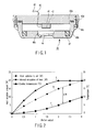
- FIG. 1 shows a conventional imaging apparatus including a cooling structure using a Peltier element.
- a solid-state imaging device 41 for imaging an image has a Peltier element 42.
- the Peltier element 42 serves as an element for cooling the solid-state imaging device 41, and its COOL surface is closely attached to the solid-state imaging device 41 and its HOT surface is closely attached to a surface of a base 43a of an exterior unit 43, respectively.
- the exterior unit 43 has the base 43a and an exterior cover 43b.
- the exterior cover 43b is provided so as to cover the periphery of the solid-state imaging device 41.
- the exterior cover 43b has a window unit 43e with opposed to the imaging surface of the solid-state imaging device 41.
- the exterior cover 43b is attached on the base 43a in airtight by a screw 43c with a packing 43d interposed therebetween.
- a cover glass 44 is disposed at the window unit 43e of the exterior cover 43b.
- the cover glass 44 adheres to the window unit 43e in airtight by means of an adhesive agent or the like.
- the lead wires 45 and 46 are connected to the solid-state imaging device 41 and the Peltier element 42, respectively.
- the lead wires 45 and 46 are guided to the outside penetrating through the base 43a of the exterior unit 43, and are connected to a power source (not shown) or the like.
- the base 43a through which the lead wires 45 and 46 penetrate are sealed by injecting a silicon resin or the like therein so as to prevent air from moving in and out.
- a silica gel 47 dries a space that is sealed by the exterior cover 43b including the solid-state imaging device 41.
- the solid-state imaging device 41 of which temperature rises upon imaging, is cooled by the Peltier element 42.
- the Peltier element 42 radiates heat that is absorbed from the solid-state imaging device 41 to the exterior unit 43, and further, the exterior unit 43 radiates the heat to air.
- the exterior unit 43 radiates the heat to air and simultaneously, also radiates the heat to an inner space of the exterior cover 43b including the solid-state imaging device 41. Therefore, the inside of the exterior cover 43b also rises in temperature, and as a result, an internal circulation of heat is generated to increase a temperature of the solid-state imaging device 41.
- Cooling of the solid-state imaging device 41 is simply represented by the following expression.
- Amount of cooling of solid-state imaging device (W) amount of heat radiation to air - amount of internal circulation of heat
- Peltier output by the Peltier element 42 is increased, and as shown in FIG. 2A, a cooling temperature of the solid-state imaging device 41 is increased.
- the temperature of the exterior unit 43 is increased, and as shown in FIG. 2B, an amount of heat radiation to air is increased.
- FIG. 2C an amount of internal circulation of heat within the exterior cover 43b is also increased, so that a cooling efficiency is deteriorated. If the Peltier output is further increased from this state, a difference ⁇ W between the amount of heat radiation to air and the amount of internal circulation of heat is saturated, and the cooling temperature of the solid-state imaging device 41 is also saturated.
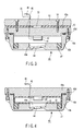
- FIG. 3 is a diagram showing a schematic configuration of an imaging apparatus disclosed in Jpn. Pat. Appln. KOKAI Publication No. 7-211823.
- FIG. 3 the same parts as FIG. 1 are given the same reference numerals.
- a COOL surface of a second Peltier element 51 is closely attached to the outside surface of the base 43a of the exterior unit 43.
- a cooling wheel 52 is closely attached on a HOT surface of the second Peltier element 51.
- a heat insulator 53 is arranged so as to surround the second Peltier element 51.
- the base 43a, the heat insulator 53, and the cooling wheel 52 are fixed in one portion by a fixing screw 54.
- a lead wire 55 is connected to the second Peltier element 51.
- Movement of heat in this case can be represented by the following expression.
- Amount of cooling of solid-state imaging device (W) amount of heat radiation to outside by cooling wheel + amount of heat radiation to outside by exterior unit - internal circulation of heat
- the solid-state imaging device 41 is intensively cooled (output to the Peltier element 42 is increased), increasing amount of heat radiation to the cooling wheel 52 by the second Peltier element 51 and making the heat radiation by the exterior unit 43 even, the internal circulation of the heat is decreased. Thereby, a cooling efficiency of the solid-state imaging device 41 is improved so as to increase a cooling temperature.
- FIG. 4 is a block schematic view of an imaging apparatus disclosed in Jpn. UM Appln. KOKOKU Publication No. 5-46381.
- FIG. 4 the same parts as FIG. 1 are given the same reference numerals.
- a heat insulator 61 is disposed on the inside surface of the base 43a of the exterior unit 43 and the inside surface of the exterior cover 43b of the exterior unit 43.
- the present invention provides an imaging apparatus capable of improving a cooling efficiency of an imaging device and further, capable of preventing dew condensation to the imaging device.
- An imaging device is characterized by comprising: an imaging device which images an image; an exterior member which contains the imaging device; an interior member which is arranged inside of the exterior member and contains the imaging device; a heat insulator arranged between the exterior member and the interior member, for thermally insulating between the exterior member and the interior member; and a cooling unit configured to cool the imaging device and the interior member respectively and radiating heat that is absorbed from the imaging device and the interior member to the exterior member independently.
- FIG. 5 is a diagram showing a schematic configuration of an imaging apparatus to which the present invention is applied.
- a solid-state imaging device 1 for imaging an image as an imaging device has a first Peltier element 2 as cooling means.
- the first Peltier element 2 serves to cool the solid-state imaging device 1, and its COOL surface is closely attached to the solid-state imaging device 1 and its HOT surface is closely attached to a surface of a base 3a of an exterior unit 3 as an exterior member, respectively.
- the exterior unit 3 contains the solid-state imaging device 1 and has an exterior cover 3b to cover the periphery of the solid-state imaging device 1.
- the exterior cover 3b has a window unit 3e with opposed to the imaging surface of the solid-state imaging device 1.
- the window unit 3e has a cover glass 4.
- the cover glass 4 adheres to the window unit 3e in airtight by means of an adhesive agent or the like.
- the exterior cover 3b is attached on the base 3a in airtight by a screw 3c via a packing 3d interposed therebetween.
- a material having a high heat conductivity for example, aluminum or copper is used as the base 3a and the exterior cover 3b configuring the exterior unit 3.
- a heat insulator 8 as heat insulator is disposed on the inside surfaces of the base 3a and the exterior cover 3b of the exterior unit 3.
- the heat insulator 8 thermally insulates between the exterior unit 3 and an internal cover 9 to be described later.
- a material having low heat conductivity for example, a resin or the like is used.
- the internal cover 9 As an interior member is arranged. Within the internal cover 9, the solid-state imaging device 1 is positioned. As the internal cover 9, a thin material having high heat conductivity is used. Such a material is used because an object of the present invention is not to cool the internal cover 9 itself but to absorb a heat from the parts or air within the internal cover 9.
- a second Peltier element 10 as cooling means is arranged between the internal cover 9 and the base 3a of the exterior unit 3.
- the second Peltier element 10 serves to cool the internal cover 9, and its COOL surface is closely attached to the internal cover 9 and its HOT surface is closely attached to the surface of the base 3a, respectively.
- the first and second Peltier elements 2 and 10, lead wires 5, 6 and 11 are connected to the solid-state imaging device 1, respectively.
- the lead wires 5, 6 and 11 are guided to the outside penetrating through the base 3a of the exterior unit 3, and are connected to a power source (not shown) or the like.
- the base 3a through which the lead wires 5, 6 and 11 penetrate are sealed by injecting a silicon resin or the like therein so as to prevent air from moving in and out through these penetrating portions.
- the silica gel 7 dries a space that is sealed by the exterior cover 3b including the solid-state imaging device 1.
- the exterior cover 3b including the solid-state imaging device 1 On the heat insulator 8 and the internal cover 9, through holes 8a and 9a are formed in a portion corresponding to the silica gel 7.
- the solid-state imaging device 1 of which temperature rises upon imaging, is cooled by the first Peltier element 2.
- the first Peltier element 2 radiates heat that is absorbed from the solid-state imaging device 1 to the base 3a of the exterior unit 3.
- the exterior unit 3 radiates the heat from the first Peltier element 2 to air and also radiates the heat to the heat insulator 8. Then, the heat insulator 8 may radiate heat slightly to the side of the internal cover 9.
- the first Peltier element 2 dedicates oneself only to the solid-state imaging device 1, so that it is possible to cool the solid-state imaging device 1 to a further lower temperature.
- the output of the first Peltier element 2 may be increased.
- the temperature of the exterior unit 3 is increased, the heat radiation to air is increased, and the heat radiation to the inside of the exterior unit 3 (the side of the internal cover 9) is also increased.
- the heat does not reach the solid-state imaging device 1, and as described above, the internal cover 9 absorbs heat to radiate it to the exterior unit 3.
- the output of the second Peltier element 10 may be increased.
- the heat radiation to the inside of the exterior unit 3 can be absorbed by the internal cover 9, and further, the internal cover 9 and an inner air layer can be cooled. As a result, it is possible to maintain a low air temperature around the solid-state imaging device 1.
- the first Peltier element 2 may be driven some time after the second Peltier element 10 is driven. In this case, water within the cover is condensed since the second Peltier element 10 is driven at first. Thereafter, when all extra water within the internal cover 9 has been condensed at the internal cover 9, the first Peltier element 2 is driven. Since all of the water within the cover is condensed on the internal cover 9, it is possible to prevent dew condensation of the image pickup surface of the solid-state imaging device 1. In this case, it is not needed to cool the internal cover 9 to a temperature that is lower than that of the solid-state imaging device 1.
- FIG. 6 is a diagram showing a schematic configuration of the second embodiment of the invention.
- the same parts as FIG. 5 are given the same reference numerals.
- an internal cover 22 is arranged via a spacer 21 made of a material having a high heat insulating efficiency.
- the spacer 21 is interposed between the exterior unit 3 and the internal cover 22 to form a narrow gap in an air layer 23 as heat insulating means.
- the air layer 23 is sealed with respect to an inner space of the internal cover 22.
- a second Peltier element 24 is arranged between the internal cover 22 and the base 3a of the exterior unit 3.
- the second Peltier element 24 serves to cool the internal cover 22, and its COOL surface is closely attached to the internal cover 22 and its HOT surface is closely attached to the surface of the base 3a, respectively.
- a lead wire 25 of the second Peltier element 24 is guided to the outside penetrating through the base 3a of the exterior unit 3, and is connected to a power source (not shown) or the like.
- the base 3a through which the lead wire 24 penetrates is sealed by injecting a silicon resin or the like therein so as to prevent air from moving in and out therethrough.
- the heat radiation to the inside of the exterior unit 3 can be absorbed by the internal cover 22, and further, the internal cover 22 itself and the inner air layer can be cooled.
- the same advantage as described in the first embodiment can be obtained.
- the air layer 23 is formed between the exterior unit 3 and the internal cover 22 via the spacer 21.
- the same advantage can be obtained.
- the above-described embodiments include the inventions at various phases, and various inventions can be extracted by an appropriate combination of plural constituent features that are disclosed here. For example, even if some constituent features are deleted from among all constituent features that are disclosed in the embodiments, it is possible to solve the problems described in "Problems to be Solved by the Invention", and if the advantages described in “Advantages of the Invention" can be obtained, the configuration having this constituent feature deleted can be extracted as the invention.
- the heat radiation from the exterior member to the inside can be absorbed by the interior member. Further, by cooling the interior member, the air inside the interior member is cooled and the air temperature around the imaging device can be maintained lower. As a result, it is possible to easily cool the imaging device to a desired low temperature and the cooling efficiency of the imaging device can be improved remarkably.
- the invention by cooling the cooled temperature of the interior member than that of the temperature of the imaging pickup device, it is possible to condense a dew inside the interior member on the interior member, so that it is possible to prevent the dew condensation on the imaging device.
Landscapes
- Engineering & Computer Science (AREA)
- Multimedia (AREA)
- Signal Processing (AREA)
- Studio Devices (AREA)
- Solid State Image Pick-Up Elements (AREA)
- Transforming Light Signals Into Electric Signals (AREA)
- Cooling Or The Like Of Semiconductors Or Solid State Devices (AREA)
Abstract
Description
Claims (5)
- An imaging apparatus characterized by comprising:an imaging device (1) which images an image;an exterior member (3) which contains the imaging device;an interior member (9, 22) which is arranged inside of the exterior member and contains the imaging device;a heat insulator (8, 23) arranged between the exterior member and the interior member, for thermally insulating between the exterior member and the interior member; anda cooling unit (2, 10) configured to cool the imaging device and the interior member respectively and radiating heat that is absorbed from the imaging device and the interior member to the exterior member independently.
- The imaging apparatus according to claim 1, characterized in that the cooling unit includes first and second Peltier elements, and the first Peltier element radiates the heat that is absorbed from the imaging device to the exterior member, and the second Peltier element radiates the heat that is absorbed from the interior member to the exterior member.
- The imaging apparatus according to claim 1 or 2, characterized in that the heat insulator includes one of a heat insulator (8), a vacuum layer, and a layer having gas filled therein (23).
- The imaging apparatus according to claim 2 or 3, characterized in that a cooled temperature of the interior member by the second Peltier element is set lower than a cooled temperature of the imaging device by the first Peltier element.
- The imaging apparatus according to claim 2 or 3, characterized in that the first Peltier element is driven after lapse of a predetermined time after driving the second Peltier element.
Applications Claiming Priority (2)
| Application Number | Priority Date | Filing Date | Title |
|---|---|---|---|
| JP2003347315 | 2003-10-06 | ||
| JP2003347315A JP4253557B2 (en) | 2003-10-06 | 2003-10-06 | Imaging device |
Publications (3)
| Publication Number | Publication Date |
|---|---|
| EP1523044A2 true EP1523044A2 (en) | 2005-04-13 |
| EP1523044A3 EP1523044A3 (en) | 2014-10-15 |
| EP1523044B1 EP1523044B1 (en) | 2018-07-18 |
Family
ID=34309188
Family Applications (1)
| Application Number | Title | Priority Date | Filing Date |
|---|---|---|---|
| EP04023807.3A Expired - Lifetime EP1523044B1 (en) | 2003-10-06 | 2004-10-06 | Imaging apparatus |
Country Status (3)
| Country | Link |
|---|---|
| US (1) | US7120025B2 (en) |
| EP (1) | EP1523044B1 (en) |
| JP (1) | JP4253557B2 (en) |
Cited By (1)
| Publication number | Priority date | Publication date | Assignee | Title |
|---|---|---|---|---|
| WO2009135539A1 (en) * | 2008-05-09 | 2009-11-12 | Robert Bosch Gmbh | Camera module with improved cooling design |
Families Citing this family (7)
| Publication number | Priority date | Publication date | Assignee | Title |
|---|---|---|---|---|
| JP2006332841A (en) * | 2005-05-24 | 2006-12-07 | Shimadzu Corp | Image sensor assembly |
| JP2007272055A (en) * | 2006-03-31 | 2007-10-18 | Olympus Corp | Imaging equipment |
| JP5147246B2 (en) * | 2007-01-19 | 2013-02-20 | キヤノン株式会社 | camera |
| JP2008242187A (en) * | 2007-03-28 | 2008-10-09 | Clarion Co Ltd | In-vehicle camera |
| JP5291892B2 (en) * | 2007-05-01 | 2013-09-18 | オリンパスイメージング株式会社 | Imaging device module, lens unit using imaging device module, and portable electronic device |
| FR3065348B1 (en) * | 2017-04-12 | 2022-06-24 | Safran Electronics & Defense | ELECTRONIC MODULE WITH IMPROVED PROTECTION AGAINST HUMIDITY |
| DE102023201942A1 (en) | 2023-03-03 | 2024-09-05 | Carl Zeiss Smt Gmbh | Peltier module, assembly and device for mask inspection |
Family Cites Families (14)
| Publication number | Priority date | Publication date | Assignee | Title |
|---|---|---|---|---|
| JPH0546381Y2 (en) | 1988-03-17 | 1993-12-03 | ||
| JP3310404B2 (en) * | 1993-07-23 | 2002-08-05 | 浜松ホトニクス株式会社 | Cooling type solid-state imaging device |
| JPH07211823A (en) * | 1994-01-24 | 1995-08-11 | Nippon Hoso Kyokai <Nhk> | Imaging device |
| JP3596029B2 (en) * | 1994-06-06 | 2004-12-02 | 住友電気工業株式会社 | Semiconductor laser module |
| JP3400114B2 (en) * | 1994-07-11 | 2003-04-28 | 株式会社東芝 | Cooling system |
| EP0741957B1 (en) * | 1994-11-30 | 2002-04-03 | Koninklijke Philips Electronics N.V. | Imaging device with anti-condensation provision |
| JP3966936B2 (en) * | 1997-01-30 | 2007-08-29 | 富士フイルム株式会社 | Cooled CCD camera |
| JPH10281864A (en) * | 1997-04-03 | 1998-10-23 | Nikon Corp | Thermal infrared camera |
| JPH11345956A (en) * | 1998-03-16 | 1999-12-14 | Canon Inc | Imaging device |
| JP2003166809A (en) * | 2001-12-03 | 2003-06-13 | Nikon Corp | Overlay inspection device |
| JP2003283174A (en) * | 2002-03-26 | 2003-10-03 | Fuji Photo Film Co Ltd | Substrate with hermetic cover |
| JP4137572B2 (en) * | 2002-09-27 | 2008-08-20 | オリンパス株式会社 | Imaging device |
| US20040169771A1 (en) * | 2003-01-02 | 2004-09-02 | Washington Richard G | Thermally cooled imaging apparatus |
| JP4782988B2 (en) * | 2004-01-15 | 2011-09-28 | オリンパス株式会社 | Imaging device |
-
2003
- 2003-10-06 JP JP2003347315A patent/JP4253557B2/en not_active Expired - Fee Related
-
2004
- 2004-10-04 US US10/957,860 patent/US7120025B2/en not_active Expired - Lifetime
- 2004-10-06 EP EP04023807.3A patent/EP1523044B1/en not_active Expired - Lifetime
Cited By (1)
| Publication number | Priority date | Publication date | Assignee | Title |
|---|---|---|---|---|
| WO2009135539A1 (en) * | 2008-05-09 | 2009-11-12 | Robert Bosch Gmbh | Camera module with improved cooling design |
Also Published As
| Publication number | Publication date |
|---|---|
| JP2005117258A (en) | 2005-04-28 |
| US20050073815A1 (en) | 2005-04-07 |
| US7120025B2 (en) | 2006-10-10 |
| EP1523044B1 (en) | 2018-07-18 |
| EP1523044A3 (en) | 2014-10-15 |
| JP4253557B2 (en) | 2009-04-15 |
Similar Documents
| Publication | Publication Date | Title |
|---|---|---|
| JP4161328B2 (en) | X-ray generator having a composite housing | |
| CN1214225C (en) | Cooling and heating device using thermoelectric module | |
| CN108207097B (en) | A thermal insulation device and electronic product | |
| EP1523044A2 (en) | Imaging apparatus | |
| WO2017145443A1 (en) | Portable radiography device | |
| JP2006292269A (en) | Cooling system | |
| US6495836B1 (en) | Two-dimensional image pickup apparatus | |
| JP2005183676A (en) | Electronic cooling unit | |
| JP2004022459A (en) | X-ray generation device | |
| JP3252902B2 (en) | Temperature control unit | |
| JP2003123999A (en) | X-ray tube device | |
| JPH0847113A (en) | Cooling structure of inverter for vehicle | |
| JP2005106381A (en) | Electronic cooling unit | |
| CN109195402B (en) | Heat sink and testing equipment | |
| JPH10146332A (en) | X-ray ct device | |
| JPH1187586A (en) | Multi-chip module cooling structure | |
| JP2002184918A (en) | Temperature control unit | |
| JPS60112297A (en) | Rotating anode x-ray tube apparatus | |
| JPH08236664A (en) | Semiconductor cooling system | |
| JP2007124805A (en) | Motor cooling structure and motor | |
| JP2007274569A (en) | Imaging device | |
| JPH088493A (en) | Heat dissipation structure in semiconductor laser device | |
| JPH07225030A (en) | Electronic dehumidifier | |
| JPH10257360A (en) | Monitoring television camera device | |
| SU1716409A1 (en) | Sensor for x-ray radiometric analyzer with semiconductor detector |
Legal Events
| Date | Code | Title | Description |
|---|---|---|---|
| PUAI | Public reference made under article 153(3) epc to a published international application that has entered the european phase |
Free format text: ORIGINAL CODE: 0009012 |
|
| AK | Designated contracting states |
Kind code of ref document: A2 Designated state(s): AT BE BG CH CY CZ DE DK EE ES FI FR GB GR HU IE IT LI LU MC NL PL PT RO SE SI SK TR |
|
| AX | Request for extension of the european patent |
Extension state: AL HR LT LV MK |
|
| PUAL | Search report despatched |
Free format text: ORIGINAL CODE: 0009013 |
|
| AK | Designated contracting states |
Kind code of ref document: A3 Designated state(s): AT BE BG CH CY CZ DE DK EE ES FI FR GB GR HU IE IT LI LU MC NL PL PT RO SE SI SK TR |
|
| AX | Request for extension of the european patent |
Extension state: AL HR LT LV MK |
|
| RIC1 | Information provided on ipc code assigned before grant |
Ipc: H04N 5/335 20110101ALI20140909BHEP Ipc: H04N 5/225 20060101ALI20140909BHEP Ipc: H01L 31/0203 20140101AFI20140909BHEP Ipc: H01L 23/38 20060101ALI20140909BHEP Ipc: H01L 31/024 20140101ALI20140909BHEP Ipc: H01L 27/146 20060101ALI20140909BHEP |
|
| 17P | Request for examination filed |
Effective date: 20141112 |
|
| 17Q | First examination report despatched |
Effective date: 20150126 |
|
| AKX | Designation fees paid |
Designated state(s): DE |
|
| AXX | Extension fees paid |
Extension state: LT Extension state: LV Extension state: HR Extension state: AL Extension state: MK |
|
| RAP1 | Party data changed (applicant data changed or rights of an application transferred) |
Owner name: OLYMPUS CORPORATION |
|
| RAP1 | Party data changed (applicant data changed or rights of an application transferred) |
Owner name: OLYMPUS CORPORATION |
|
| RIN1 | Information on inventor provided before grant (corrected) |
Inventor name: HIRANO, RYUICHI |
|
| REG | Reference to a national code |
Ref country code: DE Ref legal event code: R079 Ref document number: 602004052933 Country of ref document: DE Free format text: PREVIOUS MAIN CLASS: H01L0031020300 Ipc: H01L0027146000 |
|
| GRAP | Despatch of communication of intention to grant a patent |
Free format text: ORIGINAL CODE: EPIDOSNIGR1 |
|
| RIC1 | Information provided on ipc code assigned before grant |
Ipc: H04N 5/335 20110101ALI20171102BHEP Ipc: H04N 5/225 20060101ALI20171102BHEP Ipc: H01L 23/38 20060101ALN20171102BHEP Ipc: H01L 27/146 20060101AFI20171102BHEP Ipc: H01L 31/0203 20140101ALI20171102BHEP Ipc: H01L 31/024 20140101ALI20171102BHEP |
|
| INTG | Intention to grant announced |
Effective date: 20171128 |
|
| RIN1 | Information on inventor provided before grant (corrected) |
Inventor name: HIRANO, RYUICHI |
|
| GRAS | Grant fee paid |
Free format text: ORIGINAL CODE: EPIDOSNIGR3 |
|
| GRAA | (expected) grant |
Free format text: ORIGINAL CODE: 0009210 |
|
| AK | Designated contracting states |
Kind code of ref document: B1 Designated state(s): DE |
|
| REG | Reference to a national code |
Ref country code: DE Ref legal event code: R096 Ref document number: 602004052933 Country of ref document: DE |
|
| PGFP | Annual fee paid to national office [announced via postgrant information from national office to epo] |
Ref country code: DE Payment date: 20181029 Year of fee payment: 15 |
|
| REG | Reference to a national code |
Ref country code: DE Ref legal event code: R097 Ref document number: 602004052933 Country of ref document: DE |
|
| PLBE | No opposition filed within time limit |
Free format text: ORIGINAL CODE: 0009261 |
|
| STAA | Information on the status of an ep patent application or granted ep patent |
Free format text: STATUS: NO OPPOSITION FILED WITHIN TIME LIMIT |
|
| 26N | No opposition filed |
Effective date: 20190423 |
|
| REG | Reference to a national code |
Ref country code: DE Ref legal event code: R119 Ref document number: 602004052933 Country of ref document: DE |
|
| PG25 | Lapsed in a contracting state [announced via postgrant information from national office to epo] |
Ref country code: DE Free format text: LAPSE BECAUSE OF NON-PAYMENT OF DUE FEES Effective date: 20200501 |