EP1522151B1 - Systeme et procede relatifs a un processeur de conversion directe de porteuses multiples - Google Patents
Systeme et procede relatifs a un processeur de conversion directe de porteuses multiples Download PDFInfo
- Publication number
- EP1522151B1 EP1522151B1 EP03734443.9A EP03734443A EP1522151B1 EP 1522151 B1 EP1522151 B1 EP 1522151B1 EP 03734443 A EP03734443 A EP 03734443A EP 1522151 B1 EP1522151 B1 EP 1522151B1
- Authority
- EP
- European Patent Office
- Prior art keywords
- signal
- digital
- analog
- baseband
- carrier
- Prior art date
- Legal status (The legal status is an assumption and is not a legal conclusion. Google has not performed a legal analysis and makes no representation as to the accuracy of the status listed.)
- Expired - Lifetime
Links
- 238000006243 chemical reaction Methods 0.000 title claims description 20
- 238000000034 method Methods 0.000 title claims description 9
- 238000012545 processing Methods 0.000 claims description 11
- 238000004891 communication Methods 0.000 description 14
- 239000000969 carrier Substances 0.000 description 12
- 238000010586 diagram Methods 0.000 description 8
- 238000005070 sampling Methods 0.000 description 6
- 230000005540 biological transmission Effects 0.000 description 4
- 238000001914 filtration Methods 0.000 description 4
- 238000001228 spectrum Methods 0.000 description 4
- 238000010897 surface acoustic wave method Methods 0.000 description 4
- 239000002131 composite material Substances 0.000 description 3
- 238000005516 engineering process Methods 0.000 description 3
- 238000007493 shaping process Methods 0.000 description 3
- 239000004065 semiconductor Substances 0.000 description 2
- RYGMFSIKBFXOCR-UHFFFAOYSA-N Copper Chemical compound [Cu] RYGMFSIKBFXOCR-UHFFFAOYSA-N 0.000 description 1
- 229910000577 Silicon-germanium Inorganic materials 0.000 description 1
- 239000003570 air Substances 0.000 description 1
- 238000010420 art technique Methods 0.000 description 1
- 230000001413 cellular effect Effects 0.000 description 1
- 239000010949 copper Substances 0.000 description 1
- 229910052802 copper Inorganic materials 0.000 description 1
- 238000013461 design Methods 0.000 description 1
- 238000011161 development Methods 0.000 description 1
- 230000018109 developmental process Effects 0.000 description 1
- 230000000694 effects Effects 0.000 description 1
- 230000002452 interceptive effect Effects 0.000 description 1
- 238000004519 manufacturing process Methods 0.000 description 1
- 238000013507 mapping Methods 0.000 description 1
- 239000013307 optical fiber Substances 0.000 description 1
- 238000005192 partition Methods 0.000 description 1
- 230000005236 sound signal Effects 0.000 description 1
- 230000000153 supplemental effect Effects 0.000 description 1
Images

Classifications
-
- H—ELECTRICITY
- H04—ELECTRIC COMMUNICATION TECHNIQUE
- H04B—TRANSMISSION
- H04B1/00—Details of transmission systems, not covered by a single one of groups H04B3/00 - H04B13/00; Details of transmission systems not characterised by the medium used for transmission
- H04B1/69—Spread spectrum techniques
- H04B1/707—Spread spectrum techniques using direct sequence modulation
-
- H—ELECTRICITY
- H04—ELECTRIC COMMUNICATION TECHNIQUE
- H04L—TRANSMISSION OF DIGITAL INFORMATION, e.g. TELEGRAPHIC COMMUNICATION
- H04L5/00—Arrangements affording multiple use of the transmission path
- H04L5/02—Channels characterised by the type of signal
- H04L5/06—Channels characterised by the type of signal the signals being represented by different frequencies
-
- H—ELECTRICITY
- H03—ELECTRONIC CIRCUITRY
- H03G—CONTROL OF AMPLIFICATION
- H03G3/00—Gain control in amplifiers or frequency changers
- H03G3/20—Automatic control
- H03G3/30—Automatic control in amplifiers having semiconductor devices
- H03G3/3052—Automatic control in amplifiers having semiconductor devices in bandpass amplifiers (H.F. or I.F.) or in frequency-changers used in a (super)heterodyne receiver
-
- H—ELECTRICITY
- H04—ELECTRIC COMMUNICATION TECHNIQUE
- H04B—TRANSMISSION
- H04B1/00—Details of transmission systems, not covered by a single one of groups H04B3/00 - H04B13/00; Details of transmission systems not characterised by the medium used for transmission
- H04B1/06—Receivers
- H04B1/16—Circuits
- H04B1/30—Circuits for homodyne or synchrodyne receivers
-
- H—ELECTRICITY
- H04—ELECTRIC COMMUNICATION TECHNIQUE
- H04L—TRANSMISSION OF DIGITAL INFORMATION, e.g. TELEGRAPHIC COMMUNICATION
- H04L27/00—Modulated-carrier systems
- H04L27/32—Carrier systems characterised by combinations of two or more of the types covered by groups H04L27/02, H04L27/10, H04L27/18 or H04L27/26
- H04L27/34—Amplitude- and phase-modulated carrier systems, e.g. quadrature-amplitude modulated carrier systems
- H04L27/38—Demodulator circuits; Receiver circuits
- H04L27/3845—Demodulator circuits; Receiver circuits using non - coherent demodulation, i.e. not using a phase synchronous carrier
Definitions
- the present invention generally relates to communication systems. More specifically, the invention relates to communication systems using multiple access air interfaces and direct conversion/modulation for multi-carrier processing.
- a digital communication system typically transmits information or data using a continuous frequency carrier with modulation techniques that vary its amplitude, frequency or phase. After modulation, the signal is transmitted over a communication medium.
- the communication medium may be guided or unguided, comprising copper, optical fiber or air and is commonly referred to as the physical communication channel.
- the information to be transmitted is input in the form of a bitstream which is mapped onto a predetermined constellation of symbols that defines the modulation scheme.
- the mapping of each bit as symbols is referred to as modulation.
- WO 99/14863 discloses a broad band digital radio receiver for multicarrier signals, such as for instance TACS or GSM, employing a quadrature demodulator (DEMI/Q) to directly shift in base band the radiofrequency signal.
- DEMI/Q quadrature demodulator
- a local oscillator is used, having frequency fo placed at the centre of the radiofrequency BW band, in order that pairs of channels, symmetric versus fo are superimposed in the lower base half-band.
- the equivocation originated in the base band is then solved by second orthogonal demodulators (DEMx/y), of numeric type, which supply pairs of twice demodulated signals that can be grouped in four-equation systems in the four unknown values consisting of the components, in phase and in quadrature, of the two channels of each pair.
- DEMx/y second orthogonal demodulators
- RSCOR reconstruction networks
- US 6,351,500 discloses a method and system for the transmission and reception of a composite radio-frequency (RF) signal including a supplemental signal, preferably representing encoded digital information, together with an analog signal which represents monophonic analog audio in the AM-band.
- the analog monophonic component of the composite signal may be received by conventional AM-band audio receivers.
- the analog signal is a single-sideband large-carrier or vestigial-sideband large-carrier signal
- the composite RF signal includes a digital signal whose spectrum is substantially confined in one inner sideband.
- a baseband digital signal is combined with an analog monophonic audio signal and transmitted in upper inner and lower inner sidebands using nonlinear compatible quadrature amplitude modulation (NC-QAM).
- NC-QAM nonlinear compatible quadrature amplitude modulation
- Additional digital signals' spectrum occupies the lower outer and upper outer sidebands.
- part of the codeword information is replicated by modulated signals in both the upper outer and lower outer sidebands, preferably with diversity delay between the outer sideband signals.
- a prior art base station is typically required to utilize multiple carriers converging continguous frequency spectrum.
- a block diagram of prior art superheterodyne receiver 11 which may be implemented in the base station is shown in FIG. 1 .
- the direct conversion architecture has many inherent problems that result from downconverting the RF signal directly to baseband. These problems include self mixing which creates DC offsets in the baseband signal; even-order distortion which converts strong interfering signals to baseband: 1/f noise which is inherent in all semiconductor devices and which is inversely proportional to the frequency (f) and which masks the baseband signal; and spurious emissions of the LO signal which interferes with other users. Direct conversion receivers also stress the state-of-the-art capabilities of the analog baseband processing components because gain control and filtering must all be done at baseband. This requires expensive amplifiers that possess high dynamic range and a wide bandwidth.
- IF intermediate frequency
- DAC digital-to-analog converters
- SAW Surface Acoustic Wave
- the receiver 11 is used for digital multi-carrier wireless communication, for example a Code Division Multiple Access (CDMA) communication.
- CDMA Code Division Multiple Access
- a signal is received at the antenna 15, it passes a first bandpass filter 16 and a linear amplifier 17.
- a second bandpass filter 18 receives the signal from the amplifier 17 and provides the signal to a mixer 19.
- a local oscillator 20 is connected to the mixer 19 and the mixer 19 translates the signal from RF to IF and is then filtered by a bandpass filter 21.
- the bandpass filter 21 is connected to an ADC 22 which provides its digitized output to a digital downconverter 23.
- a complex numerically-controlled oscillator 24 is used to control the digital downconverter 23 to translate each channel at IF to baseband.
- the digital downconverter 23 provides quadrature baseband signals to a bank of finite impulse response (FIR) filters 25, which perform pulse shaping and interference rejection.
- FIR filters 25 are provided to respective digital automatic gain control circuits (DAGCs) 35 which provide outputs in four (4) respective channels 45.
- DAGCs digital automatic gain control circuits
- the digital data from each channel is sent to a digital processor (not shown) for further processing, such as data demodulation and decoding. Although four (4) channels are shown as an example, those of skill in the art would realize that there could be any number of channels.
- FIG. 2 is a block diagram showing prior art transmitter 51 using four (4) input channels Ch1-Ch4 65.
- the four (4) input channels 65 are provided to respective power control circuits 75 which, in turn, provide their outputs to respective FIR filters 85.
- the FIR filters 85 are typically used for pulse shaping purposes.
- the outputs from the FIR filters 85 are provided in quadrature to a digital up converter 95, which is connected to a complex numerically-controlled oscillator 96.
- the output of the digital up converter 95 is provided to a digital-to-analog (DAC) circuit 97, which supplies its analog output to a first bandpass filter 98, which in turn is provided to an IF mixer 99.
- DAC digital-to-analog
- the IF mixer 99 receives its local oscillator signal from an oscillator 100 and provides an output to a second bandpass filter 102.
- the output bandpass filter is amplified at an amplifier 103, filtered at an output bandpass filter 104 and provided for transmission via antenna 105.
- DC offsets The major problem with prior art direct conversion receivers is the generation of DC offsets at the output of the receiver.
- the major sources of DC offset are local oscillator self-mixing and second order intermodulation (IP2) of the mixer. DC offsets may be quite large, leading to saturation in the ADC and other performance problems in the receiver.
- IP2 second order intermodulation
- the present invention is a radio communication device, such as a receiver, transmitter or transceiver, that includes a direct conversion, multi-carrier processor.
- the multi-carrier processor frequency translates RF channels to and from a baseband using a quadrative modulator (transmitter) or demodulator (receiver). Because the analog signals are translated close to DC, conventional adjustable filters may be programmed via a bandwith control unit to support different numbers of channels (carriers) and channel bandwidths.
- This present invention enables block processing of multiple RF carriers in a wireless communication system using a direct conversion transmitter/receiver and baseband signal processing.
- Such a multi-carrier radio reduces cost by simultaneously processing multiple carriers within a single radio, rather than processing each carrier in separate radios.
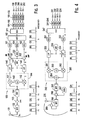
- FIG. 3 is a block diagram showing an exemplary embodiment of a communication receiver 130 constructed in accordance with the invention.
- the receiver 130 receives a plurality of communication signals Ch 1 , Ch 2 ...Ch n , each of which is sent over a carrier frequency F 1 , F 2 ...F n , respectively. These signals will be referred to collectively hereinafter as multi-carrier signal S1.
- the receiver 130 has an antenna 131, a first bandpass filter 132, a radio frequency amplifier 133 and a second bandpass filter 134. Also included are first and second mixers 141, 142, connected to a local oscillator 143, first and second low pass filters (LPFs) 145,146, a bandwidth control circuit 147 and first and second baseband amplifiers 151, 152.
- the first and second mixers 141, 142 coupled with the local oscillator 143 comprise a demodulator 144.
- a first automatic gain control (AGC) circuit 153 is connected to the baseband amplifiers 151, 152, and the outputs from the baseband amplifiers 151, 152 are provided to ADC circuits 161, 162.
- the digitized outputs from the ADCs 161, 162 are provided to a second AGC circuit 163.
- the second AGC circuit 163 provides an AGC output to a DAC 164, which in turn provides an input to the first AGC circuit 153, thereby controlling the gain of baseband amplifiers 151,152.
- the output from the second AGC circuit 163 is provided to a digital downconverter 171, which provides separate outputs to a plurality FIR filters 181-185, and in turn to a plurality DAGCs 191-195 to provide outputs to a plurality of channels Ch 1 -Ch n 198-202.
- the use of the digital-analog AGC loop 163, 164, 153 reduces the dynamic range at the output and therefore reduces the requisite dynamic range of digital AGC circuits 191-195 downstream.
- the antenna 131 captures the multi-carrier signal S1 and inputs the signal S1 to bandpass filter 132, which provides band filtering to reject out-of-band interference. After filtering, the signal is input to the low noise amplifier (LNA) 133 which sets the noise floor of the receiver 130. The output of the LNA 133 is filtered through bandpass filter (BPF) 134 to filter any intermodulation distortion produced by the LNA 133.
- LNA low noise amplifier
- BPF bandpass filter
- the output of the LNA 133 is sent to the demodulator 144, which consists of mixers 141 and 143 and the stable local oscillator (LO) 143.
- the LO 143 has two outputs, one in-phase (I) and one in quadrature (Q), relative to the carrier.
- the frequency of the LO 143 is the center frequency of the input channels Ch 1 -Ch n , (F 1 - F n )/2; where F 1 is the carrier frequency of the first channel Ch 1 and F n is the carrier frequency of the nth channel Ch n .
- the demodulator 144 translates the desired signal from RF to baseband, centering the signal around DC.
- the I and Q signals are sent to LPFs 145 and 146, which provide interference rejection in order to minimize the dynamic range of the downstream baseband processing elements 151-194. Since the analog signals are translated close to DC, conventional adjustable filters 145 and 146 may be programmed via bandwidth control 147 to support different numbers of channels and channel bandwidths.
- ADCs 161,162 are a pair of conventional low cost ADCs which digitize the I/Q signals from the demodulator 144.
- the individual channels Ch 1 -Ch n are down-converted to baseband by the DDC 171.
- Channel filtering and pulse shaping is applied to each channel Ch 1 -Ch n by the FIR filters 181-185.
- the AGC process is performed in two steps.
- the first step is performed in the first and second AGC circuits 151, 163 to adjust the gain of the baseband amplifiers 151,152 to maintain the signal within the dynamic range of the ADCs 161, 162.
- the second step of the AGC process is performed digitally in the DAGC block 191-195 and is used to reduce the bitwidth of the I/Q signals to the minimum required for each channel 198-202.
- the receiver 130 operates as a multi-carrier direct conversion receiver.
- the frequency block containing the multiple RF channels is thereby down-converted directly to baseband as a block of frequencies.
- FIG 4 is a block diagram showing an exemplary embodiment of a direct conversion communication transmitter 230 constructed in accordance with the invention.
- the individual channels (Ch 1 -Ch n ) 231-234 are first sent through FIR filters 241 -244 and are digitally upconverted by a digital upconverter DUC 247.
- This provides a digital baseband signal, which is used to drive a pair of low cost DACs 251, 252.
- the DUC 247 converts an input signal into I/Q signal components by shifting the center frequency from zero to +/- one half of the bandwidth.
- the output of the DUC 247 comprises two digital outputs which are separated in quadrature. These I/Q outputs are input to the DACs 251 and 252, which convert the digital signals to analog.
- the analog outputs from DACs 251, 252 are provided to LPFs 253, 254, the bandwidth of which are controlled by bandwidth control circuit 255.
- the LPFs 253, 254 filter the analog signals and provide their respective filtered outputs to a modulator 260, comprising two mixers 261, 262, the LO 263 and the summer 264.
- the mixers 261, 262 are controlled by the LO 263 and provide mixed outputs to the summer 264.
- the modulator 260 provides an output to the bandpass filter 265 and, in turn, to a first RF amplifier 266.
- the RF amplifier 266 is controlled by gain control circuit 267 and provides an output to bandpass filter 268 and RF power amplifier 269 which amplifies the signal for transmission, via antenna 270.
- the direct conversion multi-carrier processor in accordance with the present invention avoids the disadvantages of the superheterodyne radio by eliminating the IF stage. This reduces cost in the radio and allows the data converters to operate at baseband at a lower clock rate, which further reduces cost. Adjustable bandwidth filters are readily realizable at baseband, allowing flexible support for variable carrier spacing and the number of carriers to be processed in the radio. This also reduces the dynamic range required in the ADC because only the desired carriers are present at the ADC, again reducing cost.
- the present invention is applicable to wireless communication systems, including wireless local loop, wireless LAN applications, and cellular systems such as WCDMA (both UTRATDD and UTRAFDD), TDSCDMA, CDMA2000, 3xRT, and OFDMA systems.
- WCDMA both UTRATDD and UTRAFDD
- TDSCDMA Time Division Multiple Access
- CDMA2000 Code Division Multiple Access2000
- 3xRT Code Division Multiple Access 2000
- OFDMA OFDMA
Landscapes
- Engineering & Computer Science (AREA)
- Signal Processing (AREA)
- Computer Networks & Wireless Communication (AREA)
- Digital Transmission Methods That Use Modulated Carrier Waves (AREA)
- Transceivers (AREA)
- Transmitters (AREA)
Claims (5)
- Récepteur de conversion directe à porteuses multiples (130) pour recevoir et traiter un signal de fréquence radio, RF, à porteuses multiples, comprenant:une antenne (131) pour recevoir le signal RF à porteuses multiples;un amplificateur RF (133) configuré pour s'interfacer entre l'antenne (131) et un démodulateur (144) et amplifier le signal RF à porteuses multiples reçu;le démodulateur (144) étant couplé à l'amplificateur RF (133) et configuré pour convertir le signal RF à porteuses multiples en signaux de bande de base en phase, I, et en quadrature, Q ;un premier et un second convertisseur analogique à numérique (161, 162), le premier convertisseur (161) état configuré pour convertir le signal de bande de base I en un signal numérique I et le second convertisseur (162) étant configuré pour convertir le signal de bande de base Q en un signal numérique Q ; etun circuit de conversion directe (171) connecté aux convertisseurs analogique à numérique (161, 162) pour convertir les signaux numériques I et Q en une pluralité de signaux de canal (198 - 202) ;caractérisé par :un premier et un second étages de bande de base, chaque étage comprenant un filtre passe-bas (145, 146) et un amplificateur de gain ajustable (151, 152), le premier étage étant configuré pour traiter le signal de bande de base I et le second étage étant configuré pour traiter le signal de bande de base Q, dans lequel la bande passante de chacun des filtres passe-bas (145, 146) est ajustable ; etun circuit de commande de bande passante (147) pour commander la bande passante des filtres passe-bas.
- Récepteur (130) selon la revendication 1, comprenant en outre une pluralité de filtres à réponse impulsionnelles finie, FIR, (181- 185), chacun de la pluralité de filtres étant configuré pour filtrer un signal respectif de ladite pluralité de signaux de canal.
- Emetteur de modulation directe à porteuses multiples (230) pour traiter et transmettre une pluralité de signaux de canal (231 - 234), l'émetteur de modulation directe à porteuses multiples (230) pour traiter et transmettre une pluralité de signaux de canal (231 ur comprenant :un convertisseur numérique à la hausse (247), configuré pour recevoir ladite pluralité de signaux de canal et délivrer un signal numérique en phase, I, correspondant à ladite pluralité de signaux de canal (231, 232, 233, 234) et un signal numérique en quadrature, Q, correspondant à ladite pluralité de signaux de canal (231, 232, 233, 234);un premier et un second convertisseurs numérique à analogique (251, 253), le premier convertisseur (251) étant configuré pour convertir ledit signal numérique I en un signal analogique I à une fréquence de bande de base et le second convertisseur (252) étant configuré pour convertir ledit signal numérique Q en un signal analogique Q à une fréquence de bande de base ;un modulateur (260) configuré pour moduler lesdits signaux numériques de bande de base I et Q afin de fournir un signal de fréquence radio mixte, RF ; etune antenne (270) configurée pour transmettre ledit signal RF,caractérisé parun premier et un second filtres passe-bas (253, 254), ledit premier filtre (253) étant couplé audit premier convertisseur numérique à analogique (251) et configuré pour filtrer ledit signala analogique I e ledit second filtre (254) étant couplé audit second convertisseur numérique à analogique (252) et configuré pour filtrer ledit signal analogique Q, dans lequel la bande passante de chacun des filtres passe-bas (253, 254) est ajustable ;un circuit de commande de bande de base (255) configuré pour commander la réponse de fréquence de l'émetteur en commandant la bande passante desdits filtres passe-bas (253, 254).
- Emetteur (230) selon la revendication 3, incluant un amplificateur RF (269) configuré pour amplifier ledit signal RF.
- Emetteur (230) selon la revendication 3, incluant une pluralité de filtres à réponse impulsionnelle finie, FIR, (241 - 244), chaque filtre FIR étant configuré pour recevoir un de ladite pluralité de signaux de canal (241, 242, 243, 244) et fournir une sortie filtrée correspondante à un signal de canal respectif du convertisseur numérique à la hausse (247).
Priority Applications (1)
| Application Number | Priority Date | Filing Date | Title |
|---|---|---|---|
| EP16154053.9A EP3032755A1 (fr) | 2002-06-07 | 2003-06-05 | Système et procédé pour un processeur de conversion directe de porteuses multiples |
Applications Claiming Priority (3)
| Application Number | Priority Date | Filing Date | Title |
|---|---|---|---|
| US38720702P | 2002-06-07 | 2002-06-07 | |
| US387207P | 2002-06-07 | ||
| PCT/US2003/017851 WO2003105390A2 (fr) | 2002-06-07 | 2003-06-05 | Systeme et procede relatifs a un processeur de conversion directe de porteuses multiples |
Related Child Applications (2)
| Application Number | Title | Priority Date | Filing Date |
|---|---|---|---|
| EP16154053.9A Division-Into EP3032755A1 (fr) | 2002-06-07 | 2003-06-05 | Système et procédé pour un processeur de conversion directe de porteuses multiples |
| EP16154053.9A Division EP3032755A1 (fr) | 2002-06-07 | 2003-06-05 | Système et procédé pour un processeur de conversion directe de porteuses multiples |
Publications (3)
| Publication Number | Publication Date |
|---|---|
| EP1522151A2 EP1522151A2 (fr) | 2005-04-13 |
| EP1522151A4 EP1522151A4 (fr) | 2006-05-17 |
| EP1522151B1 true EP1522151B1 (fr) | 2016-03-23 |
Family
ID=29736279
Family Applications (2)
| Application Number | Title | Priority Date | Filing Date |
|---|---|---|---|
| EP16154053.9A Withdrawn EP3032755A1 (fr) | 2002-06-07 | 2003-06-05 | Système et procédé pour un processeur de conversion directe de porteuses multiples |
| EP03734443.9A Expired - Lifetime EP1522151B1 (fr) | 2002-06-07 | 2003-06-05 | Systeme et procede relatifs a un processeur de conversion directe de porteuses multiples |
Family Applications Before (1)
| Application Number | Title | Priority Date | Filing Date |
|---|---|---|---|
| EP16154053.9A Withdrawn EP3032755A1 (fr) | 2002-06-07 | 2003-06-05 | Système et procédé pour un processeur de conversion directe de porteuses multiples |
Country Status (12)
| Country | Link |
|---|---|
| US (2) | US7162218B2 (fr) |
| EP (2) | EP3032755A1 (fr) |
| JP (1) | JP4152944B2 (fr) |
| KR (3) | KR100671364B1 (fr) |
| CN (2) | CN101425811A (fr) |
| AR (1) | AR040160A1 (fr) |
| AU (1) | AU2003238923A1 (fr) |
| CA (1) | CA2488740A1 (fr) |
| MX (1) | MXPA04012249A (fr) |
| NO (1) | NO20045559L (fr) |
| TW (3) | TW200715777A (fr) |
| WO (1) | WO2003105390A2 (fr) |
Cited By (1)
| Publication number | Priority date | Publication date | Assignee | Title |
|---|---|---|---|---|
| CN113454939A (zh) * | 2019-04-30 | 2021-09-28 | 华为技术有限公司 | 一种探测参考信号的发送方法及相关装置 |
Families Citing this family (38)
| Publication number | Priority date | Publication date | Assignee | Title |
|---|---|---|---|---|
| DE60111056T2 (de) * | 2001-10-26 | 2006-05-04 | Stmicroelectronics N.V. | Direktmischempfänger für einem Kommunikationssystem mit nicht konstanter Hüllkurve |
| DE10253671B3 (de) * | 2002-11-18 | 2004-08-19 | Infineon Technologies Ag | Unterdrückung der Nachbarkanalinterferenz durch adaptive Kanalfilterung in Mobilfunkempfängern |
| EP1434345B1 (fr) * | 2002-12-18 | 2011-03-02 | Texas Instruments Incorporated | Récepteur de télécommunication avec commande automatique de gain |
| US7995684B2 (en) * | 2003-02-01 | 2011-08-09 | Qualcomm, Incorporated | Method and apparatus for automatic gain control of a multi-carrier signal in a communication receiver |
| US20050053127A1 (en) * | 2003-07-09 | 2005-03-10 | Muh-Tian Shiue | Equalizing device and method |
| US7869528B2 (en) * | 2003-10-31 | 2011-01-11 | Northrop Grumman Systems Corporation | Multi-carrier transceiver assembly |
| US7664520B2 (en) * | 2004-06-24 | 2010-02-16 | Nokia Corporation | Low current direct conversion transmitter architecture |
| JP4708076B2 (ja) * | 2005-04-14 | 2011-06-22 | 三星電子株式会社 | ダウンコンバータ及びアップコンバータ |
| US8000302B2 (en) | 2005-06-23 | 2011-08-16 | Qualcomm Incorporated | Adaptive multi-channel modem |
| US7477879B1 (en) * | 2005-06-30 | 2009-01-13 | Silicon Laboratories, Inc. | Transceiver system with common receiver and transmitter oscillator |
| US8693525B2 (en) | 2006-07-14 | 2014-04-08 | Qualcomm Incorporated | Multi-carrier transmitter for wireless communication |
| US8295371B2 (en) | 2006-07-14 | 2012-10-23 | Qualcomm Incorporated | Multi-carrier receiver for wireless communication |
| KR100789784B1 (ko) | 2006-10-11 | 2007-12-28 | 한국전자통신연구원 | 스케일러블 대역폭을 지원하는 수신 장치 및 그 방법 |
| WO2008044868A1 (fr) * | 2006-10-11 | 2008-04-17 | Electronics And Telecommunications Research Institute | Récepteur et procédé de réception pour largeur de bande évolutive |
| US7826815B2 (en) * | 2007-07-13 | 2010-11-02 | Fairchild Semiconductor Corporation | Dynamic selection of oscillation signal frequency for power converter |
| US7945217B2 (en) * | 2007-11-13 | 2011-05-17 | Provigent Ltd. | Multi-mode baseband-IF converter |
| FI20075958A0 (fi) | 2007-12-21 | 2007-12-21 | Nokia Corp | Lähetettävien signaalien prosessointi radiolähettimessä |
| US7991368B2 (en) * | 2007-12-27 | 2011-08-02 | Provigent Ltd | Integrated RF-IF converter |
| GB2458908B (en) * | 2008-04-01 | 2010-02-24 | Michael Frank Castle | Low power signal processor |
| WO2010013091A1 (fr) * | 2008-07-28 | 2010-02-04 | Freescale Semiconductor, Inc. | Unité de communication sans fil pour dispositif à semi-conducteur et procédé de réception d'un signal |
| US20100119008A1 (en) * | 2008-11-11 | 2010-05-13 | Flexiradio, Llc | Programmable wide band digital receiver/transmitter |
| US8514982B2 (en) * | 2008-12-12 | 2013-08-20 | CSR Technology, Inc | Systems and methods for digitizing multiple channels in a receiver |
| KR101489964B1 (ko) * | 2009-09-01 | 2015-02-06 | 한국전자통신연구원 | 수신 장치 및 수신 방법 |
| EP2290828B1 (fr) | 2009-09-01 | 2016-11-09 | Electronics and Telecommunications Research Institute | Appareil et procédé de réception |
| US20110053536A1 (en) * | 2009-09-03 | 2011-03-03 | Provigent Ltd | Receiver with re-demodulation |
| US8547207B2 (en) * | 2010-03-11 | 2013-10-01 | Checkpoint System, Inc. | RFID converter module |
| DE102010027566A1 (de) * | 2010-05-18 | 2011-11-24 | Rohde & Schwarz Gmbh & Co. Kg | Signalgenerator mit digitaler Zwischenfrequenz und digitaler Frequenzfeineinstellung |
| US8903330B2 (en) | 2010-12-13 | 2014-12-02 | Huawei Technologies Co., Ltd. | Communication signal transmission method, device and system |
| CN102104392B (zh) | 2010-12-15 | 2013-10-09 | 华为技术有限公司 | 多频段多路收发设备及方法、基站系统 |
| US8406709B2 (en) | 2011-02-27 | 2013-03-26 | Provigent Ltd. | Carrier recovery in re-modulation communication systems |
| KR101947066B1 (ko) * | 2011-09-15 | 2019-02-12 | 인텔 코포레이션 | 전치 왜곡 선형화 통신 시스템 및 송신기의 전치 왜곡 선형화 방법 |
| EP2573997A1 (fr) * | 2011-09-26 | 2013-03-27 | Thomson Licensing | Procédé de contrôle de la bande passante et dispositif correspondant |
| GB2504973B (en) * | 2012-08-15 | 2014-11-19 | Broadcom Corp | Receiver circuit |
| KR101367236B1 (ko) * | 2013-06-24 | 2014-02-26 | 주식회사 삼정솔루션 | Trs전파보호장치 |
| CN105048966A (zh) * | 2015-06-12 | 2015-11-11 | 中国电子科技集团公司第四十一研究所 | 一种千兆赫高速采样信号的多相数字下变频方法 |
| US10191454B2 (en) * | 2016-06-13 | 2019-01-29 | William Marsh Rice University | Methods and related systems of ultra-short pulse detection |
| EP3746385A4 (fr) | 2018-02-02 | 2021-10-27 | ATS Automation Tooling Systems Inc. | Système de transporteur à moteur linéaire pour environnements propres/aseptiques |
| KR102426630B1 (ko) * | 2022-04-12 | 2022-07-28 | 한화시스템(주) | 저궤도 위성의 rf 신호 처리 장치 및 그 방법 |
Family Cites Families (35)
| Publication number | Priority date | Publication date | Assignee | Title |
|---|---|---|---|---|
| US4654800A (en) * | 1984-02-20 | 1987-03-31 | Kabushikikaisha Nippon Coinco | Control and monitoring apparatus for vending machines |
| US5095536A (en) * | 1990-03-23 | 1992-03-10 | Rockwell International Corporation | Direct conversion receiver with tri-phase architecture |
| KR970007983B1 (ko) * | 1992-06-08 | 1997-05-19 | 모토로라 인코포레이티드 | 자동 이득 제어 회로 및 수신기 |
| FR2707063B1 (fr) * | 1993-06-25 | 1995-09-22 | Alcatel Mobile Comm France | |
| US5519732A (en) * | 1994-05-02 | 1996-05-21 | Harris Corporation | Digital baseband to IF conversion in cellular base stations |
| JPH0832464A (ja) * | 1994-07-15 | 1996-02-02 | Uniden Corp | 送信機におけるキャリアリーク補正方法 |
| US5715314A (en) * | 1994-10-24 | 1998-02-03 | Open Market, Inc. | Network sales system |
| US5758257A (en) * | 1994-11-29 | 1998-05-26 | Herz; Frederick | System and method for scheduling broadcast of and access to video programs and other data using customer profiles |
| US5579341A (en) * | 1994-12-29 | 1996-11-26 | Motorola, Inc. | Multi-channel digital transceiver and method |
| US7937312B1 (en) * | 1995-04-26 | 2011-05-03 | Ebay Inc. | Facilitating electronic commerce transactions through binding offers |
| US6009130A (en) * | 1995-12-28 | 1999-12-28 | Motorola, Inc. | Multiple access digital transmitter and receiver |
| FI112133B (fi) * | 1996-03-29 | 2003-10-31 | Nokia Corp | Menetelmä kahdella eri taajuuusalueella toimivan radioviestinjärjestelmän suoramuunnoslähetin/vastaanottimen taajuuksien muodostamiseksi ja kahdella taajuusalueella toimivan radioviestinjärjestelmänsuoramuunnoslähetin/vastaanotin sekä edellisten käyttö matkaviestimessä |
| KR0164419B1 (ko) * | 1996-04-19 | 1999-02-01 | 김광호 | 무선 수신기의 자동 이득 제어회로 |
| US5898912A (en) * | 1996-07-01 | 1999-04-27 | Motorola, Inc. | Direct current (DC) offset compensation method and apparatus |
| US6005894A (en) * | 1997-04-04 | 1999-12-21 | Kumar; Derek D. | AM-compatible digital broadcasting method and system |
| US6029052A (en) * | 1997-07-01 | 2000-02-22 | Telefonaktiebolaget Lm Ericsson | Multiple-mode direct conversion receiver |
| IT1294284B1 (it) * | 1997-07-29 | 1999-03-24 | Italtel Spa | Radiotrasmettitore a larga banda per un segnale costituito da una pluralita' di portanti equispaziate modulate digitalmente |
| IT1297278B1 (it) * | 1997-09-15 | 1999-08-09 | Italtel Spa | Radioricevitore digitale a larga banda per segnale multiportante |
| AUPP261898A0 (en) * | 1998-03-27 | 1998-04-23 | Victoria University Of Technology | Dc offset and im2 removal in direct conversion receivers |
| CN1120602C (zh) * | 1998-04-14 | 2003-09-03 | 弗兰霍菲尔运输应用研究公司 | 多载波解调系统中精细频率同步化的方法及装置 |
| JP3319422B2 (ja) * | 1998-05-08 | 2002-09-03 | 日本電気株式会社 | マルチキャリア伝送システム、マルチキャリア伝送方法 |
| US7106689B1 (en) * | 1999-03-02 | 2006-09-12 | Matsushita Electric Industrial Co., Ltd. | OFDM transmission/reception apparatus |
| US7149726B1 (en) * | 1999-06-01 | 2006-12-12 | Stamps.Com | Online value bearing item printing |
| JP3551841B2 (ja) * | 1999-06-09 | 2004-08-11 | 日本電気株式会社 | 受信機及びその利得制御方法 |
| US6480528B1 (en) * | 1999-06-11 | 2002-11-12 | Qualcomm Incorporated | Automatic gain control for improved decoding of multi-carrier signal |
| US6631170B1 (en) * | 1999-12-03 | 2003-10-07 | Nokia Corporation | Radio frequency receiver |
| US7213005B2 (en) * | 1999-12-09 | 2007-05-01 | International Business Machines Corporation | Digital content distribution using web broadcasting services |
| JP4652546B2 (ja) * | 2000-09-21 | 2011-03-16 | 三星電子株式会社 | 受信機 |
| US6560448B1 (en) * | 2000-10-02 | 2003-05-06 | Intersil Americas Inc. | DC compensation system for a wireless communication device configured in a zero intermediate frequency architecture |
| US7260141B2 (en) * | 2001-02-28 | 2007-08-21 | Itt Manufacturing Enterprises, Inc. | Integrated beamformer/modem architecture |
| US20020127982A1 (en) * | 2001-03-07 | 2002-09-12 | Nokia Mobile Phones Ltd | Mobile station receiver operable for both single and multi-carrier reception |
| KR100446540B1 (ko) * | 2001-04-16 | 2004-09-01 | 삼성전자주식회사 | 데이터 통신용 송신기 |
| US7243153B2 (en) * | 2001-06-26 | 2007-07-10 | Eastman Kodak Company | System and method for managing images over a communication network |
| US20030078011A1 (en) * | 2001-10-18 | 2003-04-24 | Integrated Programmable Communications, Inc. | Method for integrating a plurality of radio systems in a unified transceiver structure and the device of the same |
| US6819910B2 (en) * | 2002-03-08 | 2004-11-16 | Broadcom Corp. | Radio employing a self calibrating transmitter with reuse of receiver circuitry |
-
2003
- 2003-06-05 MX MXPA04012249A patent/MXPA04012249A/es active IP Right Grant
- 2003-06-05 KR KR1020047019912A patent/KR100671364B1/ko not_active IP Right Cessation
- 2003-06-05 TW TW095119778A patent/TW200715777A/zh unknown
- 2003-06-05 TW TW093104385A patent/TWI320637B/zh not_active IP Right Cessation
- 2003-06-05 WO PCT/US2003/017851 patent/WO2003105390A2/fr active Application Filing
- 2003-06-05 CA CA002488740A patent/CA2488740A1/fr not_active Abandoned
- 2003-06-05 CN CNA2008101660484A patent/CN101425811A/zh active Pending
- 2003-06-05 KR KR1020087013473A patent/KR20080059339A/ko not_active Application Discontinuation
- 2003-06-05 EP EP16154053.9A patent/EP3032755A1/fr not_active Withdrawn
- 2003-06-05 AU AU2003238923A patent/AU2003238923A1/en not_active Abandoned
- 2003-06-05 CN CNB038131463A patent/CN100426690C/zh not_active Expired - Fee Related
- 2003-06-05 JP JP2004512332A patent/JP4152944B2/ja not_active Expired - Fee Related
- 2003-06-05 TW TW092115312A patent/TWI237450B/zh not_active IP Right Cessation
- 2003-06-05 KR KR1020057017487A patent/KR20050096208A/ko not_active Application Discontinuation
- 2003-06-05 EP EP03734443.9A patent/EP1522151B1/fr not_active Expired - Lifetime
- 2003-06-06 US US10/456,300 patent/US7162218B2/en not_active Expired - Lifetime
- 2003-06-06 AR ARP030102016A patent/AR040160A1/es active IP Right Grant
-
2004
- 2004-12-20 NO NO20045559A patent/NO20045559L/no not_active Application Discontinuation
-
2006
- 2006-11-22 US US11/562,802 patent/US20070085718A1/en not_active Abandoned
Cited By (4)
| Publication number | Priority date | Publication date | Assignee | Title |
|---|---|---|---|---|
| CN113454939A (zh) * | 2019-04-30 | 2021-09-28 | 华为技术有限公司 | 一种探测参考信号的发送方法及相关装置 |
| EP3944540A1 (fr) * | 2019-04-30 | 2022-01-26 | Huawei Technologies Co., Ltd. | Procédé d'envoi de signal de référence de sondage, et appareil associé |
| EP3944540A4 (fr) * | 2019-04-30 | 2022-04-13 | Huawei Technologies Co., Ltd. | Procédé d'envoi de signal de référence de sondage, et appareil associé |
| CN113454939B (zh) * | 2019-04-30 | 2023-03-03 | 华为技术有限公司 | 一种探测参考信号的发送方法及相关装置 |
Also Published As
| Publication number | Publication date |
|---|---|
| TWI237450B (en) | 2005-08-01 |
| TW200400700A (en) | 2004-01-01 |
| NO20045559L (no) | 2004-12-20 |
| EP1522151A2 (fr) | 2005-04-13 |
| KR20080059339A (ko) | 2008-06-26 |
| JP4152944B2 (ja) | 2008-09-17 |
| AU2003238923A8 (en) | 2003-12-22 |
| CA2488740A1 (fr) | 2003-12-18 |
| TWI320637B (en) | 2010-02-11 |
| KR20050014850A (ko) | 2005-02-07 |
| JP2005529544A (ja) | 2005-09-29 |
| AR040160A1 (es) | 2005-03-16 |
| CN101425811A (zh) | 2009-05-06 |
| US20070085718A1 (en) | 2007-04-19 |
| US20040072547A1 (en) | 2004-04-15 |
| EP3032755A1 (fr) | 2016-06-15 |
| CN100426690C (zh) | 2008-10-15 |
| CN1706109A (zh) | 2005-12-07 |
| TW200501594A (en) | 2005-01-01 |
| WO2003105390A3 (fr) | 2004-04-01 |
| WO2003105390A2 (fr) | 2003-12-18 |
| KR20050096208A (ko) | 2005-10-05 |
| TW200715777A (en) | 2007-04-16 |
| MXPA04012249A (es) | 2005-02-25 |
| EP1522151A4 (fr) | 2006-05-17 |
| AU2003238923A1 (en) | 2003-12-22 |
| KR100671364B1 (ko) | 2007-01-22 |
| US7162218B2 (en) | 2007-01-09 |
Similar Documents
| Publication | Publication Date | Title |
|---|---|---|
| EP1522151B1 (fr) | Systeme et procede relatifs a un processeur de conversion directe de porteuses multiples | |
| JP5608939B2 (ja) | 受信機、送信機、フィードバックデバイス、送受信機および信号処理方法 | |
| US7092676B2 (en) | Shared functional block multi-mode multi-band communication transceivers | |
| US7769359B2 (en) | Adaptive wireless receiver | |
| US20020176522A1 (en) | Quadrature envelope-sampling of intermediate frequency signal in receiver | |
| US7924802B2 (en) | Wireless communication systems and methods | |
| KR100736057B1 (ko) | 듀얼 디지털 저역 if 복합 수신기 | |
| US11031962B2 (en) | Carrier aggregated signal transmission and reception | |
| JP4589331B2 (ja) | マルチモード・マルチバンド送受信機 | |
| US5703910A (en) | Digital radio receiver | |
| KR100527844B1 (ko) | 초고주파 송수신 장치 | |
| JP2002290367A (ja) | 帯域分割復調方法及びofdm受信機 | |
| Bada et al. | Design and realisation of digital radio transceiver using software radio architecture | |
| Efstathiou et al. | Enabling components for multi-standard software radio base stations | |
| JOSHI | Software Defined Radio |
Legal Events
| Date | Code | Title | Description |
|---|---|---|---|
| PUAI | Public reference made under article 153(3) epc to a published international application that has entered the european phase |
Free format text: ORIGINAL CODE: 0009012 |
|
| 17P | Request for examination filed |
Effective date: 20050107 |
|
| AK | Designated contracting states |
Kind code of ref document: A2 Designated state(s): AT BE BG CH CY CZ DE DK EE ES FI FR GB GR HU IE IT LI LU MC NL PT RO SE SI SK TR |
|
| AX | Request for extension of the european patent |
Extension state: AL LT LV MK |
|
| DAX | Request for extension of the european patent (deleted) | ||
| A4 | Supplementary search report drawn up and despatched |
Effective date: 20060404 |
|
| 17Q | First examination report despatched |
Effective date: 20061108 |
|
| RAP1 | Party data changed (applicant data changed or rights of an application transferred) |
Owner name: INTERDIGITAL TECHNOLOGY CORPORATION |
|
| GRAP | Despatch of communication of intention to grant a patent |
Free format text: ORIGINAL CODE: EPIDOSNIGR1 |
|
| INTG | Intention to grant announced |
Effective date: 20141119 |
|
| GRAP | Despatch of communication of intention to grant a patent |
Free format text: ORIGINAL CODE: EPIDOSNIGR1 |
|
| INTG | Intention to grant announced |
Effective date: 20150420 |
|
| REG | Reference to a national code |
Ref country code: DE Ref legal event code: R079 Ref document number: 60348709 Country of ref document: DE Free format text: PREVIOUS MAIN CLASS: H04B0001707000 Ipc: H04B0001300000 |
|
| GRAP | Despatch of communication of intention to grant a patent |
Free format text: ORIGINAL CODE: EPIDOSNIGR1 |
|
| RIC1 | Information provided on ipc code assigned before grant |
Ipc: H04L 27/38 20060101ALI20150907BHEP Ipc: H03G 3/30 20060101ALI20150907BHEP Ipc: H04B 1/30 20060101AFI20150907BHEP Ipc: H04L 5/06 20060101ALI20150907BHEP Ipc: H04L 27/26 20060101ALI20150907BHEP |
|
| INTG | Intention to grant announced |
Effective date: 20150930 |
|
| GRAS | Grant fee paid |
Free format text: ORIGINAL CODE: EPIDOSNIGR3 |
|
| GRAA | (expected) grant |
Free format text: ORIGINAL CODE: 0009210 |
|
| AK | Designated contracting states |
Kind code of ref document: B1 Designated state(s): AT BE BG CH CY CZ DE DK EE ES FI FR GB GR HU IE IT LI LU MC NL PT RO SE SI SK TR |
|
| REG | Reference to a national code |
Ref country code: GB Ref legal event code: FG4D |
|
| REG | Reference to a national code |
Ref country code: CH Ref legal event code: EP |
|
| REG | Reference to a national code |
Ref country code: AT Ref legal event code: REF Ref document number: 784042 Country of ref document: AT Kind code of ref document: T Effective date: 20160415 |
|
| REG | Reference to a national code |
Ref country code: IE Ref legal event code: FG4D |
|
| REG | Reference to a national code |
Ref country code: DE Ref legal event code: R096 Ref document number: 60348709 Country of ref document: DE |
|
| REG | Reference to a national code |
Ref country code: NL Ref legal event code: FP |
|
| REG | Reference to a national code |
Ref country code: FR Ref legal event code: PLFP Year of fee payment: 14 |
|
| PG25 | Lapsed in a contracting state [announced via postgrant information from national office to epo] |
Ref country code: GR Free format text: LAPSE BECAUSE OF FAILURE TO SUBMIT A TRANSLATION OF THE DESCRIPTION OR TO PAY THE FEE WITHIN THE PRESCRIBED TIME-LIMIT Effective date: 20160624 |
|
| REG | Reference to a national code |
Ref country code: AT Ref legal event code: MK05 Ref document number: 784042 Country of ref document: AT Kind code of ref document: T Effective date: 20160323 |
|
| PG25 | Lapsed in a contracting state [announced via postgrant information from national office to epo] |
Ref country code: SE Free format text: LAPSE BECAUSE OF FAILURE TO SUBMIT A TRANSLATION OF THE DESCRIPTION OR TO PAY THE FEE WITHIN THE PRESCRIBED TIME-LIMIT Effective date: 20160323 |
|
| PG25 | Lapsed in a contracting state [announced via postgrant information from national office to epo] |
Ref country code: EE Free format text: LAPSE BECAUSE OF FAILURE TO SUBMIT A TRANSLATION OF THE DESCRIPTION OR TO PAY THE FEE WITHIN THE PRESCRIBED TIME-LIMIT Effective date: 20160323 |
|
| PG25 | Lapsed in a contracting state [announced via postgrant information from national office to epo] |
Ref country code: ES Free format text: LAPSE BECAUSE OF FAILURE TO SUBMIT A TRANSLATION OF THE DESCRIPTION OR TO PAY THE FEE WITHIN THE PRESCRIBED TIME-LIMIT Effective date: 20160323 Ref country code: SK Free format text: LAPSE BECAUSE OF FAILURE TO SUBMIT A TRANSLATION OF THE DESCRIPTION OR TO PAY THE FEE WITHIN THE PRESCRIBED TIME-LIMIT Effective date: 20160323 Ref country code: AT Free format text: LAPSE BECAUSE OF FAILURE TO SUBMIT A TRANSLATION OF THE DESCRIPTION OR TO PAY THE FEE WITHIN THE PRESCRIBED TIME-LIMIT Effective date: 20160323 Ref country code: PT Free format text: LAPSE BECAUSE OF FAILURE TO SUBMIT A TRANSLATION OF THE DESCRIPTION OR TO PAY THE FEE WITHIN THE PRESCRIBED TIME-LIMIT Effective date: 20160725 Ref country code: RO Free format text: LAPSE BECAUSE OF FAILURE TO SUBMIT A TRANSLATION OF THE DESCRIPTION OR TO PAY THE FEE WITHIN THE PRESCRIBED TIME-LIMIT Effective date: 20160323 Ref country code: CZ Free format text: LAPSE BECAUSE OF FAILURE TO SUBMIT A TRANSLATION OF THE DESCRIPTION OR TO PAY THE FEE WITHIN THE PRESCRIBED TIME-LIMIT Effective date: 20160323 |
|
| PG25 | Lapsed in a contracting state [announced via postgrant information from national office to epo] |
Ref country code: IT Free format text: LAPSE BECAUSE OF FAILURE TO SUBMIT A TRANSLATION OF THE DESCRIPTION OR TO PAY THE FEE WITHIN THE PRESCRIBED TIME-LIMIT Effective date: 20160323 Ref country code: BE Free format text: LAPSE BECAUSE OF FAILURE TO SUBMIT A TRANSLATION OF THE DESCRIPTION OR TO PAY THE FEE WITHIN THE PRESCRIBED TIME-LIMIT Effective date: 20160323 |
|
| REG | Reference to a national code |
Ref country code: DE Ref legal event code: R097 Ref document number: 60348709 Country of ref document: DE |
|
| PLBE | No opposition filed within time limit |
Free format text: ORIGINAL CODE: 0009261 |
|
| STAA | Information on the status of an ep patent application or granted ep patent |
Free format text: STATUS: NO OPPOSITION FILED WITHIN TIME LIMIT |
|
| PG25 | Lapsed in a contracting state [announced via postgrant information from national office to epo] |
Ref country code: DK Free format text: LAPSE BECAUSE OF FAILURE TO SUBMIT A TRANSLATION OF THE DESCRIPTION OR TO PAY THE FEE WITHIN THE PRESCRIBED TIME-LIMIT Effective date: 20160323 Ref country code: MC Free format text: LAPSE BECAUSE OF FAILURE TO SUBMIT A TRANSLATION OF THE DESCRIPTION OR TO PAY THE FEE WITHIN THE PRESCRIBED TIME-LIMIT Effective date: 20160323 |
|
| REG | Reference to a national code |
Ref country code: CH Ref legal event code: PL |
|
| PG25 | Lapsed in a contracting state [announced via postgrant information from national office to epo] |
Ref country code: BG Free format text: LAPSE BECAUSE OF FAILURE TO SUBMIT A TRANSLATION OF THE DESCRIPTION OR TO PAY THE FEE WITHIN THE PRESCRIBED TIME-LIMIT Effective date: 20160623 |
|
| 26N | No opposition filed |
Effective date: 20170102 |
|
| PG25 | Lapsed in a contracting state [announced via postgrant information from national office to epo] |
Ref country code: LI Free format text: LAPSE BECAUSE OF NON-PAYMENT OF DUE FEES Effective date: 20160630 Ref country code: CH Free format text: LAPSE BECAUSE OF NON-PAYMENT OF DUE FEES Effective date: 20160630 |
|
| REG | Reference to a national code |
Ref country code: FR Ref legal event code: PLFP Year of fee payment: 15 |
|
| PG25 | Lapsed in a contracting state [announced via postgrant information from national office to epo] |
Ref country code: SI Free format text: LAPSE BECAUSE OF FAILURE TO SUBMIT A TRANSLATION OF THE DESCRIPTION OR TO PAY THE FEE WITHIN THE PRESCRIBED TIME-LIMIT Effective date: 20160323 |
|
| REG | Reference to a national code |
Ref country code: FR Ref legal event code: PLFP Year of fee payment: 16 |
|
| PG25 | Lapsed in a contracting state [announced via postgrant information from national office to epo] |
Ref country code: HU Free format text: LAPSE BECAUSE OF FAILURE TO SUBMIT A TRANSLATION OF THE DESCRIPTION OR TO PAY THE FEE WITHIN THE PRESCRIBED TIME-LIMIT; INVALID AB INITIO Effective date: 20030605 Ref country code: CY Free format text: LAPSE BECAUSE OF FAILURE TO SUBMIT A TRANSLATION OF THE DESCRIPTION OR TO PAY THE FEE WITHIN THE PRESCRIBED TIME-LIMIT Effective date: 20160323 |
|
| PG25 | Lapsed in a contracting state [announced via postgrant information from national office to epo] |
Ref country code: TR Free format text: LAPSE BECAUSE OF FAILURE TO SUBMIT A TRANSLATION OF THE DESCRIPTION OR TO PAY THE FEE WITHIN THE PRESCRIBED TIME-LIMIT Effective date: 20160323 Ref country code: LU Free format text: LAPSE BECAUSE OF NON-PAYMENT OF DUE FEES Effective date: 20160605 |
|
| PGFP | Annual fee paid to national office [announced via postgrant information from national office to epo] |
Ref country code: NL Payment date: 20220627 Year of fee payment: 20 Ref country code: IE Payment date: 20220621 Year of fee payment: 20 Ref country code: GB Payment date: 20220621 Year of fee payment: 20 |
|
| PGFP | Annual fee paid to national office [announced via postgrant information from national office to epo] |
Ref country code: FI Payment date: 20220621 Year of fee payment: 20 |
|
| PGFP | Annual fee paid to national office [announced via postgrant information from national office to epo] |
Ref country code: FR Payment date: 20220623 Year of fee payment: 20 |
|
| PGFP | Annual fee paid to national office [announced via postgrant information from national office to epo] |
Ref country code: DE Payment date: 20220628 Year of fee payment: 20 |
|
| REG | Reference to a national code |
Ref country code: DE Ref legal event code: R071 Ref document number: 60348709 Country of ref document: DE |
|
| REG | Reference to a national code |
Ref country code: NL Ref legal event code: MK Effective date: 20230604 |
|
| P01 | Opt-out of the competence of the unified patent court (upc) registered |
Effective date: 20230514 |
|
| REG | Reference to a national code |
Ref country code: GB Ref legal event code: PE20 Expiry date: 20230604 |
|
| REG | Reference to a national code |
Ref country code: IE Ref legal event code: MK9A |
|
| PG25 | Lapsed in a contracting state [announced via postgrant information from national office to epo] |
Ref country code: IE Free format text: LAPSE BECAUSE OF EXPIRATION OF PROTECTION Effective date: 20230605 Ref country code: GB Free format text: LAPSE BECAUSE OF EXPIRATION OF PROTECTION Effective date: 20230604 |