EP1519472B1 - Elektrochirurgisches Schaltnetzteil - Google Patents
Elektrochirurgisches Schaltnetzteil Download PDFInfo
- Publication number
- EP1519472B1 EP1519472B1 EP04022423.0A EP04022423A EP1519472B1 EP 1519472 B1 EP1519472 B1 EP 1519472B1 EP 04022423 A EP04022423 A EP 04022423A EP 1519472 B1 EP1519472 B1 EP 1519472B1
- Authority
- EP
- European Patent Office
- Prior art keywords
- power supply
- output
- supply apparatus
- circuit
- frequency
- Prior art date
- Legal status (The legal status is an assumption and is not a legal conclusion. Google has not performed a legal analysis and makes no representation as to the accuracy of the status listed.)
- Expired - Lifetime
Links
Images



Classifications
-
- H—ELECTRICITY
- H02—GENERATION; CONVERSION OR DISTRIBUTION OF ELECTRIC POWER
- H02M—APPARATUS FOR CONVERSION BETWEEN AC AND AC, BETWEEN AC AND DC, OR BETWEEN DC AND DC, AND FOR USE WITH MAINS OR SIMILAR POWER SUPPLY SYSTEMS; CONVERSION OF DC OR AC INPUT POWER INTO SURGE OUTPUT POWER; CONTROL OR REGULATION THEREOF
- H02M1/00—Details of apparatus for conversion
- H02M1/12—Arrangements for reducing harmonics from AC input or output
-
- H—ELECTRICITY
- H02—GENERATION; CONVERSION OR DISTRIBUTION OF ELECTRIC POWER
- H02M—APPARATUS FOR CONVERSION BETWEEN AC AND AC, BETWEEN AC AND DC, OR BETWEEN DC AND DC, AND FOR USE WITH MAINS OR SIMILAR POWER SUPPLY SYSTEMS; CONVERSION OF DC OR AC INPUT POWER INTO SURGE OUTPUT POWER; CONTROL OR REGULATION THEREOF
- H02M3/00—Conversion of DC power input into DC power output
- H02M3/22—Conversion of DC power input into DC power output with intermediate conversion into AC
- H02M3/24—Conversion of DC power input into DC power output with intermediate conversion into AC by static converters
- H02M3/28—Conversion of DC power input into DC power output with intermediate conversion into AC by static converters using discharge tubes with control electrode or semiconductor devices with control electrode to produce the intermediate AC
- H02M3/325—Conversion of DC power input into DC power output with intermediate conversion into AC by static converters using discharge tubes with control electrode or semiconductor devices with control electrode to produce the intermediate AC using devices of a triode or a transistor type requiring continuous application of a control signal
- H02M3/335—Conversion of DC power input into DC power output with intermediate conversion into AC by static converters using discharge tubes with control electrode or semiconductor devices with control electrode to produce the intermediate AC using devices of a triode or a transistor type requiring continuous application of a control signal using semiconductor devices only
- H02M3/33569—Conversion of DC power input into DC power output with intermediate conversion into AC by static converters using discharge tubes with control electrode or semiconductor devices with control electrode to produce the intermediate AC using devices of a triode or a transistor type requiring continuous application of a control signal using semiconductor devices only having several active switching elements
- H02M3/33573—Full-bridge at primary side of an isolation transformer
Definitions
- the present invention relates to a power supply apparatus for electric operation which is preferably used for an electric operation apparatus.
- an electric operation apparatus is frequently used for treatments for incising or coagulating the affected portion by applying high-frequency current.
- Fig. 7 shows the structure of an electric operation apparatus 21 according to a conventional art.
- the electric operation apparatus 21 comprises: a power supply apparatus 23 which receives the commercial power supply by its connection to the commercial power supply 22; high-frequency generating circuit 24 which generates a high-frequency output based on a DC power output supplied from the power supply apparatus 23; a sensor circuit 25 which detects the voltage level and the current level of the high-frequency output that is outputted from the high-frequency generating circuit 24; and a CPU circuit 26 which controls the power supply apparatus 23 and the high-frequency generating circuit 24 based on the detected result that is inputted from the sensor circuit 25.
- the high-frequency output of the high-frequency generating circuit 24 is connected to a high-frequency output connector portion 27 via the sensor circuit 25, and performs the treatment such as the incision and coagulation by feeding (outputting) the high-frequency current to a high-frequency cautery treatment tool (also referred to as a high-frequency electric scalpel) connected to the high-frequency output connector portion 27.
- a high-frequency cautery treatment tool also referred to as a high-frequency electric scalpel
- the CPU circuit 26 outputs an output voltage instructing signal (for controlling and) for instructing the output voltage to the power supply apparatus 23 based on the detected result of the sensor circuit 25.
- the power supply apparatus 23 receives the output voltage instructing signal from the CPU circuit 26 and supplies, to the high-frequency generating circuit 24, the DC power output in accordance with the output voltage instructing signal.
- the high-frequency generating circuit 24 generates the high-frequency output based on the DC power output supplied from the power supply apparatus 23.
- the power supply apparatus 23 comprises: a PFC circuit (power factor improving circuit) 31; a DC/DC converter circuit 32; and a control circuit 33.
- the PFC circuit 31 effectively converts, into DC power, AC power inputted from the commercial power supply 22.
- the DC/DC converter circuit 32 generates the DC high-voltage output (power output) in accordance with the output voltage instructing signal which is inputted from the control circuit 33, and feeds the power output from its output terminal to the high-frequency generating circuit 24.
- the control circuit 33 compares the output voltage instructing signal inputted from the CPU circuit 26 with an output voltage FB signal which is obtained by feeding back an output voltage of the power output, and outputs, to the DC/DC converter circuit 32, a signal for controlling the driving the DC/DC converter circuit 32 (specifically, switching element driving signal) based on the compared signal.
- Fig. 8 shows the specific structure of the control circuit 33 shown in Fig. 7 and the DC/DC converter circuit 32.
- the DC/DC converter circuit 32 comprises: an FET bridge (switching element bridge) 41 having field-effect transistors (hereinafter, abbreviated to FETs) Q1 to Q4; an insulating transfer 42; a diode bridge 43; and an output smoothing filter 44.
- FET bridge switching element bridge
- the FET bridge 41 receives the DC power from the PFC circuit 31.
- the FET bridge 41 is connected to a primary wiring of the insulating transfer 42, and executes the switching operation, thereby transmitting the power to a secondary wiring.
- the diode bridge 43 is connected to the secondary wiring of the insulating transfer 42, the pulsating flow shaped by the diode bridge 43 is smoothed by the output smoothing filter 44 comprising a choke coil and a condenser.
- the smoothed DC power output is supplied to the high-frequency generating circuit 24.
- a negative line in the power output is connected to a patient circuit ground (abbreviated to a patient GND in Figs. 7 and 8 ).
- the power output is divided to two DC voltages with proper levels via two dividing resistors Ra and Rb, then, one voltage is inputted to one input terminal of an error amplifier 45 of the control circuit 33 as an output voltage feedback signal (abbreviated to an output voltage FB signal), and another voltage is inputted to another input terminal of the error amplifier 45 as a reference output voltage instructing signal.
- an output voltage feedback signal abbreviated to an output voltage FB signal
- the error amplifier 45 outputs the compared result of both the input signals as an error amplifier output signal to a PWM control circuit (pulse width modulation control circuit) 46.
- the PWM control circuit 46 outputs a switching element driving signal with pulse widths varied depending on a voltage value of the error-amplifier output.
- the switching element driving signal is applied to gates of the FET Q1 to Q4 forming the FET bridge 41 via an insulating element 47. Consequently, the FET bridge 41 is switched (on/off).
- Drains of the FET Q1 and Q2 are connected to the positive output terminal of the PFC circuit 31, and sources of the FET Q1 and Q2 are connected to drains of the FET Q3 and Q4.
- Sources of the FET Q3 AND Q4 are connected to a primary circuit ground (abbreviated to the primary GND in Fig. 8 ).
- the sources of the FET Q1 and Q2 are connected to both ends of the primary wiring of the insulating transfer 42, and the diode bridge 43 comprising four diodes is connected to the secondary wiring.
- the output voltage instructing signal and the output voltage FB signal are inputted to the error amplifier 45.
- the output voltage FB signal is obtained by dividing the power output by the resistors and therefore the voltage value changes in proportion to the power output.
- the error amplifier 45 compares the output voltage FB signal with the reference output voltage instructing signal, and outputs the compared result to the PWM control circuit 46.
- the PWM control circuit 46 includes a comparator 48 which compares the output of the error amplifier with reference zigzag waves, and outputs the compared result as a switching element driving signal.
- the PWM control circuit 46 when the voltage of the reference zigzag waves are higher than the voltage of the output of the error amplifier, the PWM control circuit 46 outputs the switching element driving signal. Then, the switching element driving signal is transmitted to the FET Q1 to Q4 forming the FET bridge 41 of the DC/DC converter circuit 32 via the insulating element 47.
- the power is transmitted to the secondary wiring via the insulating transfer 42.
- the transmitted power is shaped by the diode bridge 43 and further the DC power output smoothed by the output smoothing filter 44 is supplied to the high-frequency generating circuit 24.
- the DC/DC converter circuit 32 supplies, to the high-frequency generating circuit 24, the power output in accordance with the output voltage instructing signal.
- the output smoothing filter 44 for smoothing the output voltage is arranged to the output terminal of the DC/DC converter circuit 32.
- the output smoothing filter 44 functions as a low path filter and therefore reduces a cut-off frequency as a capacitance Cb of a smoothing capacitor and inductance Lb of the choke coil are higher.
- the cut-off frequency of the output smoothing filter 44 is reduced and the response speed is slow, thereby removing the noises included in the power output.
- the electric operation apparatus needs to response to the fluctuation of the output setting or load (patient tissue) at the high speed.
- the cut-off frequency of the output smoothing filter 44 is reduced and therefore the response speed is not fast.
- the electric operation apparatus comprises the high-frequency generating circuit 24 therein.
- the noises generated in the high-frequency generating circuit 24 propagate into the electric operation apparatus.
- the noises mixed in the output voltage instructing signal pass through the error amplifier 45 and then a signal including the noises is inputted to the PMW control circuit 46.
- the frequency or pulse width of a switching element driving signal outputted from the PWM control circuit 46 is irregular.
- the cut-off frequency of 500 Hz or more the power output is not stably supplied.
- the noises included in the power output of the power supply apparatus 23 propagate in the output voltage instructing signal and mix in the control circuit 33 in the power supply apparatus 23, as shown by a dotted line.
- the noises pull out from the high-frequency generating circuit 24 propagate in the power output or output voltage instructing signal, and mix in the control circuit 33 of the power supply apparatus 23 as shown by the dotted line.
- noises propagate in the wiring. Further, the noises are radiated to another wiring from the wiring including the noises and are propagated.
- control circuit 33 of the power supply apparatus 23 is apart from a frame ground (FG) connected to the earth. Therefore, it has a problem of a normal-mode noise and a common-mode noise.
- the normal-mode noise is a noise which flows to a line on the ground (GND) side as the negative from the positive line of the output voltage instructing signal, and has different phase in both the lines.
- the common-mode noise is a noise which flows to a frame ground (FG) from the output voltage instructing signal, and has the same phase in both the lines of the output voltage instructing signal.
- PCT international publication No. 98/07378 discloses an electric operation apparatus. However, it has the same drawback as that shown in Fig. 7 according to the conventional art.
- a power supply apparatus according to claim 1 is provided.
- an electric operation apparatus 1 comprises a high-frequency output connector portion 27 in front of a casing.
- a connector 4 of a cable 3 connected to a high-frequency electric scalpel 2 is detachably connected to the high-frequency output connector portion 27.
- a foot switch 5 is connected to the electric operation apparatus 1, and instructs the on/off operation of the high-frequency output.
- An operating panel 6 of the electric operation apparatus 1 has an incision mode setting portion 7a and a coagulating mode setting portion 7b so as to output the high frequency with an output waveform suitable to the medical treatment such as the incision or coagulation, in accordance therewith, and displays an output setting and an output value in the incision mode setting portion 7a and the coagulating mode setting portion 7b.
- the high-frequency electric scalpel 2 performs a medical treatment such as incision or coagulation on a patient 9 that is placed on an operation bed 8.
- a bi-polar system high-frequency electric scalpel 2 is briefly shown in Fig. 1
- a mono-polar system high-frequency electric scalpel may be connected and used with an opposite-polar plate.
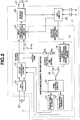
- Fig. 2 shows the internal structure of the electric operation apparatus 1.
- the electric operation apparatus 1 comprises: the power supply apparatus 11 according to the first embodiment; a high-frequency generating circuit 24; a sensor circuit 25; and a CPU circuit 26.
- the foot switch 5 and the operating panel 6 are connected to the CPU circuit 26.
- the electric operation apparatus 1 shown in Fig. 2 uses the power supply apparatus 11, in place of the power supply apparatus 23 shown in Fig. 7 .
- the power supply apparatus 11 comprises: a PFC circuit 31; a DC/DC converter circuit 12; and a control circuit 13. Similarly to Fig. 7 , the PFC circuit 31 converts AC power supplied from the commercial power supply 22 into DC power, and supplies the converted power to the DC/DC converter circuit 12.
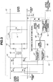
- the DC/DC converter circuit 12 and the control circuit 13 in the power supply apparatus 11 according to the first embodiment has the structure shown in Fig. 3 .
- the DC/DC converter circuit 12 is obtained by using an output smoothing filter (or low path filter) 14 comprising a capacitor with a capacitance Ca and a choke coil with inductance La for obtaining a higher cut-off frequency (specifically, 500 Hz or more), in place of the output smoothing filter 44, in the DC/DC converter circuit 32 shown in Fig. 8 and by connecting the patient circuit GND of the DC/DC converter circuit 12 to a frame ground (abbreviated to an FG) via a capacitor 15 as capacitor connecting means.
- an output smoothing filter or low path filter 14 comprising a capacitor with a capacitance Ca and a choke coil with inductance La for obtaining a higher cut-off frequency (specifically, 500 Hz or more)
- the capacitor 15 uses a capacitor with such preferable frequency property that the impedance is low up to the higher frequency, such as a laminated ceramic capacitor.
- a capacitor with such preferable frequency property that the impedance is low up to the higher frequency such as a laminated ceramic capacitor.
- a non-laminated ceramic capacitor, a polyester film capacitor, a polystyrene capacitance, and a mica capacitor may be used.
- the capacitance of the capacitor 15 is, e.g., 1,000 pF.
- the DC/DC converter circuit 12 comprises: a field-effect transistor (hereinafter, abbreviated to FET) bridge (switching element bridge) 41 comprising filed-effect transistors (hereinafter, abbreviated to FETs) Q1 to Q4; an insulating transfer 42; a diode bridge 43; and the output smoothing filter 14.
- FET field-effect transistor
- switching element bridge switching element bridge
- the DC current is supplied (inputted) to the FET bridge 41 from the PFC circuit 31.
- the FET bridge 41 is connected to the primary wiring of the insulating transfer 42, and the FET bridge 41 is switched on, thereby transmitting the power to the secondary wiring.
- the diode bridge 43 is connected to the secondary wiring of the insulating transfer 42.
- the pulsating flow shaped by the diode bridge 43 is smoothed by the output smoothing filter 14 comprising the choke coil and the capacitor.
- the smoothed DC power output is supplied to the high-frequency generating circuit 24.
- the negative line of the power output is connected to a patient circuit ground (abbreviated to the patient GND in Figs. 2 and 3 ).
- the power output is divided to two DC voltages with proper levels via two dividing resistors Ra and Rb, and the voltages are inputted to one input terminal of an error amplifier 45 of the control circuit 13, as output voltage feedback signals (abbreviated to output voltage FB signals).
- a reference output voltage instructing signal is inputted to another input terminal of the error amplifier 45 via the normal-mode noise/common-mode noise removing circuit 16.
- the error amplifier 45 outputs, to a PWM control circuit (pulse width modulation control circuit) 46, the compared results of the two input signals as error amplifier output signals.
- the PWM control circuit 46 outputs switching element driving signals with varied pulse widths, in accordance with the voltage level of the error amplifier output.
- the switching element driving signal is applied to gates of the FETs Q1 to Q4 forming the FET bridge 41 via the insulating element 47 such as a pulse transfer.
- the FET bridge 41 is switched on/off.
- Drains of the FETs Q1 and Q2 are connected to a positive output terminal of the PFC circuit 31.
- Sources of the FETs Q1 and Q2 are connected to drains of the FETs Q3 and Q4.
- Sources of the FETs Q3 and Q4 are connected to the primary-circuit ground (abbreviated to the primary GND in Fig. 3 ).
- the sources of the FETs Q1 and Q2 are connected to both ends of the primary wiring of the insulating transfer 42, and the diode bridge 43 comprising four diodes are connected to the secondary wiring of the insulating transfer 42.
- the control circuit 13 comprises a normal-mode noise/common-mode noise removing circuit 16, as noise removing means (noise reducing means), which removes or reduces a normal-mode noise (also referred to as a differential-mode noise) and a common-mode noise at a signal input portion which receives the output voltage instructing signal.
- noise removing means noise reducing means
- the input terminal of the error amplifier 45 receives the output voltage FB signal which is obtained by dividing the power output of the DC/DC converter circuit 12 by the resistors Ra and Rb and an output signal of the normal-mode noise/common-mode noise removing circuit 16 whose input terminal receives the output voltage instructing signal.
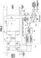
- Fig. 4 shows the main portion of the power supply apparatus 11, as the normal-mode noise/common-mode noise removing circuit 16 shown in Fig. 3 , including the control circuit 13 using a differential amplifier circuit 16A.
- the differential amplifier circuit 16A is arranged to the signal input portion of the control circuit 13, thereby removing or reducing the normal-mode noises and the common-mode noises in the control circuit 13.
- the output voltage instructing signal is inputted to the non-inverting and inverting input terminals of the differential amplifier circuit 16A via resistors R1 and R2.
- the non-inverting input terminal of the differential amplifier circuit 16A is connected to the ground of the power output via a resistor R3.
- the inverting input terminal is connected to an output terminal of the differential amplifier circuit 16A via a resistor R4.
- the output terminal of the differential amplifier circuit 16A is connected to the error amplifier 45.
- the response speed is improved by setting, to be higher, the cut-off frequency of the output smoothing filter 14 in the DC/DC converter circuit 12. Since the cut-off frequency of the output smoothing filter 14 is set to be higher, the noises increase.
- the common-mode noises are reduced by connecting the ground of the output terminal of the DC/DC converter circuit 12 to a frame ground (abbreviated to an FG) via capacitor connecting means and further noise removing means is arranged to remove or reduce the normal-mode noises and the common-mode noises to the signal input portion of the control circuit 13. Consequently, the noise mixing in the control circuit 13 is suppressed.
- the error amplifier 45 as the signal input portion of the control circuit 13 receives the output voltage FB signal which is obtained by dividing the output voltage of the DC/DC converter circuit 12 and the output voltage instructing signal via the normal-mode noise/common-mode noise removing circuit 16.
- the output voltage FB signal inputted to the error amplifier 45 is a signal which is obtained by diving the power output by resistors and therefore the voltage level of the signal changes in proportion to the power output.
- the error amplifier 45 compares the reference output voltage instructing signal with the output voltage FB signal and then outputs the compared result to the PWM control circuit 46.
- the PWM control circuit 46 comprises the comparator 48 which compares the error amplifier output with the reference zigzag wave. Further, the PWM control circuit 46 outputs the compared result as the switching element driving signal.
- the PWM control circuit 46 when the voltage of the reference zigzag wave is higher than the voltage of the error amplifier output, the PWM control circuit 46 outputs the switching element driving signal. Then, the switching element driving signal is transmitted to the FETs Q1 to Q4 forming the FET bridge 41 of the DC/DC converter circuit 12 via the insulating element 47.
- the power is transmitted to the secondary wiring via the insulating transfer 42.
- the transmitted power is shaped by the diode bridge 43 and further the DC power output smoothed by the output smoothing filter 14 is supplied to the high-frequency generating circuit 24.
- the DC/DC converter circuit 12 supplies, to the high-frequency generating circuit 24, the power output in accordance with the output voltage instructing signal.
- the cut-off frequency of the output smoothing filter 14 is set to be higher, the noises increase.
- the noise mixing is suppressed as follows.
- the capacitor 15 couples the FG (ground) and the ground of the power output of the DC/DC converter circuit 12.
- the GND potential of the power output is more stable, as compared with that according to the conventional art, thus to reduce the normal-mode noise and common-mode noise which are mixed to the signal input portion of the control circuit 13, from the power output.
- the impedance is reduced between the ground of the power output and the FG. Further, the normal-mode noise and common-mode noise mixed to the positive line via the capacitor (its capacitance Ca) forming the output smoothing filter 14 are reduced.
- the differential amplifier circuit 16A is arranged to the signal input portion in the control circuit 13 as shown in Fig. 4 .
- the common-mode noises are reduced as follows and the generation of normal-mode noises is suppressed in the control circuit 13.
- reference symbol Vin denotes the output voltage instructing signal, and it is assumed that the common-mode noise is mixed to the output voltage instructing signal Vin.
- the use of the differential amplifier circuit 16A enables the reduction of the common-mode noises mixed in the output voltage instructing signal.
- the common-mode noises are removed in the signal input portion of the control circuit 13, thus, the generating of normal-mode noises is suppressed in the control circuit 13 and the common-mode noise and the normal-mode noise are removed or are reduced.
- CMRR common mode rejection ratio
- the influence of the frequency property of CMRR enables the more reduction of noise removing property as the frequency is higher. Further, the deterioration of noise removing property is prevented with the cut-off frequency (e.g., 500 Hz or more) of the output smoothing filter 14.
- the cut-off frequency e.g., 500 Hz or more
- a capacitor with preferable frequency property may be used, e.g., the laminated ceramic capacitor.
- the necessary insulating property is assured and the common-mode noise and the normal-mode noise are reduced.
- the response speed is improved by increasing the cut-off frequency of the output smoothing filter 14 in the DC/DC converter circuit 12, and the noises are reduced and the stable operation is realized by arranging the noise removing means.
- the response speed of the power output is not delayed because of the reduction of noises, but both the fast response and the noise reduction are established.
- the fast speed of the power supply apparatus 11 is ensured and the treatments such as the incision of the high-frequency electric scalpel and the coagulating are properly performed without noises.
- the response property of the power output is further improved as compared with the conventional art. Therefore, when the treatments change the organ of the patient, the power output is supplied in fast response to the change. The more proper power-supply is possible.
- the reliability for the power supply apparatus 11 and the electric operation apparatus is improved.
- Fig. 5 shows the structure of a main portion of a power supply apparatus according to the second embodiment.
- an instrumentation amplifier circuit 16B is used as the normal-mode noise/common-mode noise removing circuit 16.
- the non-inverting input terminal of the instrumentation amplifier circuit 16B is connected to the ground of the power output via a resistor R3.
- the inverting input terminal of the instrumentation amplifier circuit 16B is connected to the output terminal thereof.
- reference symbol Vin denotes the output voltage instructing signal and reference symbol Vn denotes the common-mode noise.
- Vin+Vn the signals applied to the non-inverting input terminal and inverting input terminal of the instrumentation amplifier circuit 16B are expressed by (Vin+Vn) and Vn, respectively.
- the normal-mode noises are suppressed in the control circuit 13.
- the removing property of the instrumentation amplifier circuit 16B is determined depending on the CMRR of the instrumentation amplifier circuit 16B.
- the CMRR of the instrumentation amplifier circuit 16B is further higher (normally, higher by several tens dB), as compared with the case of the differential amplifier circuit 16A.
- the property for removing the noises is further improved.
- the noise removing property is reduced.
- the reduction of the noise removing property is prevented up to the frequency that is equal to the cut-off frequency or more of the output smoothing filter 14.
- the second embodiment has the same advantages as those according to the first embodiment and the function for reducing or removing the noises is improved.
- a normal-mode noise/common-mode noise removing circuit 16C comprises a common-mode choke coil 20.
- the common-mode choke coil 20 operates as the choke coil, only for the same phase signal (current).
- the output voltage instructing signal is inputted and then the current in one signal line of the common-mode choke coil 20 is opposite to the current in another feedback line. Therefore, the magnetic fluxes generated in the common-mode choke coil 20 are mutually negated, that is, this state is close to the non-insertion of the choke coil.
- the common-mode choke coil by using the common-mode choke coil, the common-mode noise mixed in the output voltage instructing signal are removed. Further, by removing the common-mode noises in the input portion of the control circuit 13, the generation of the normal-mode noises is suppressed in the control circuit 13.
- the noise removing property using the common-mode choke coil 20 is determined depending on the inductance of the common-mode choke coil 20. Further, the noise removing property is reduced by the frequency higher than the resonant frequency under the influence of the stray capacitance of the wiring and the inductance. However, the influence of the inductance and the stray capacitance of the wiring is reduced by setting the resonant frequency of the common-mode choke coil 20 to be higher than the one of the cut-off frequency of the output smoothing filter 14.
Landscapes
- Engineering & Computer Science (AREA)
- Power Engineering (AREA)
- Dc-Dc Converters (AREA)
- Surgical Instruments (AREA)
Claims (9)
- Energiezufuhrgerät (11) für ein elektrisches Operationsgerät (1), das dazu eingerichtet ist, eine Gleichspannungsausgabespannung an einen Hochfrequenzerzeugungsschaltkreis (24) auszugeben, wobei das Energiezufuhrgerät (11) umfasst:einen Ausgabeglättungsfilter (14), der dazu eingerichtet ist, eine Gleichspannung zu glätten, wobei die geglättete Gleichspannung an den Hochfrequenzerzeugungsschaltkreis (24) ausgegeben wird, um ein Hochfrequenzsignal zu erzeugen; undeinen Fehlerverstärker (45), der dazu eingerichtet ist, ein Ausgabespannungs-Feedbacksignal mit einem Ausgabespannungs-Befehlssignal zu vergleichen;dadurch gekennzeichnet, dassdie Frequenzobergrenze des Ausgabeglättungsfilters (14) auf 500 Hz oder mehr festgelegt ist, so dass eine Reaktionsgeschwindigkeit des Energiezufuhrgeräts verbessert wird, und dassdas Energiezufuhrgerät ein Störungsreduktionsmittel (16; 16A, 16B, 16C) zur Reduktion von zumindest einer Common-Mode-Störung umfasst, wobei das Störungsreduktionsmittel (16; 16A, 16B, 16C) mit einem Eingangsanschluss des Fehlerverstärkers (45) verbunden und dazu eingerichtet ist, das Ausgabespannungs-Befehlssignal zu empfangen.
- Energiezufuhrgerät (11) nach Anspruch 1, dadurch gekennzeichnet, dass das Störungsreduktionsmittel (16) dazu eingerichtet ist, eine Normal-Mode-Störung und eine Common-Mode-Störung zu reduzieren.
- Energiezufuhrgerät (11) nach Anspruch 1, das ferner dadurch gekennzeichnet ist, dass es umfasst:ein Kapazitätskopplungsmittel (15), das dazu eingerichtet ist, eine Kapazität zwischen eine Masse an einem Ausgangsanschluss der Ausgabespannung und eine geerdete Gehäusemasse zu koppeln.
- Energiezufuhrgerät (11) nach Anspruch 1, dadurch gekennzeichnet, dass das Störungsreduktionsmittel (16A) einen Differenzialverstärker umfasst.
- Energiezufuhrgerät (11) nach Anspruch 4, dadurch gekennzeichnet, dass das Störungsreduktionsmittel (16B) einen Instrumentationsverstärker umfasst, der Pufferverstärker (19a, 19b) umfasst, die über Widerstände (R1, R2) verbunden sind, die Widerstandswerte haben, die jeweils gleich denjenigen eines invertierten Eingangsanschlusses und eines nicht-invertierten Eingangsanschlusses des Differenzialverstärkers (16A) sind.
- Energiezufuhrgerät (11) nach Anspruch 1, dadurch gekennzeichnet, dass das Störungsreduktionsmittel (16C) eine Common-Mode-Drosselspule (20) umfasst.
- Energiezufuhrgerät (11) nach Anspruch 3, dadurch gekennzeichnet, dass das Kapazitätskopplungsmittel ein Kondensator (15) mit einer vorbestimmten Frequenzeigenschaft ist.
- Energiezufuhrgerät (11) nach Anspruch 7, dadurch gekennzeichnet, dass der Kondensator (15) ein keramischer Kondensator oder ein laminierter keramischer Kondensator ist.
- Energiezufuhrgerät (11) für eine elektrische Operation nach Anspruch 7, dadurch gekennzeichnet, dass der Kondensator einen Kondensator (15) mit ungefähr 1000 pF hat.
Applications Claiming Priority (2)
| Application Number | Priority Date | Filing Date | Title |
|---|---|---|---|
| JP2003336547 | 2003-09-26 | ||
| JP2003336547A JP2005102750A (ja) | 2003-09-26 | 2003-09-26 | 電気手術用電源装置 |
Publications (2)
| Publication Number | Publication Date |
|---|---|
| EP1519472A1 EP1519472A1 (de) | 2005-03-30 |
| EP1519472B1 true EP1519472B1 (de) | 2017-03-08 |
Family
ID=34191540
Family Applications (1)
| Application Number | Title | Priority Date | Filing Date |
|---|---|---|---|
| EP04022423.0A Expired - Lifetime EP1519472B1 (de) | 2003-09-26 | 2004-09-21 | Elektrochirurgisches Schaltnetzteil |
Country Status (3)
| Country | Link |
|---|---|
| US (1) | US7324357B2 (de) |
| EP (1) | EP1519472B1 (de) |
| JP (1) | JP2005102750A (de) |
Families Citing this family (59)
| Publication number | Priority date | Publication date | Assignee | Title |
|---|---|---|---|---|
| US6033399A (en) * | 1997-04-09 | 2000-03-07 | Valleylab, Inc. | Electrosurgical generator with adaptive power control |
| US7364577B2 (en) | 2002-02-11 | 2008-04-29 | Sherwood Services Ag | Vessel sealing system |
| US7901400B2 (en) | 1998-10-23 | 2011-03-08 | Covidien Ag | Method and system for controlling output of RF medical generator |
| US7137980B2 (en) | 1998-10-23 | 2006-11-21 | Sherwood Services Ag | Method and system for controlling output of RF medical generator |
| US8133218B2 (en) | 2000-12-28 | 2012-03-13 | Senorx, Inc. | Electrosurgical medical system and method |
| US6620157B1 (en) | 2000-12-28 | 2003-09-16 | Senorx, Inc. | High frequency power source |
| US20050004559A1 (en) | 2003-06-03 | 2005-01-06 | Senorx, Inc. | Universal medical device control console |
| US7044948B2 (en) | 2002-12-10 | 2006-05-16 | Sherwood Services Ag | Circuit for controlling arc energy from an electrosurgical generator |
| CA2524289C (en) * | 2003-05-01 | 2016-01-19 | Sherwood Services Ag | Method and system for programming and controlling an electrosurgical generator system |
| EP1676108B1 (de) | 2003-10-23 | 2017-05-24 | Covidien AG | Schaltung für thermoelement-messsignalen |
| US7396336B2 (en) * | 2003-10-30 | 2008-07-08 | Sherwood Services Ag | Switched resonant ultrasonic power amplifier system |
| US7131860B2 (en) * | 2003-11-20 | 2006-11-07 | Sherwood Services Ag | Connector systems for electrosurgical generator |
| US7628786B2 (en) * | 2004-10-13 | 2009-12-08 | Covidien Ag | Universal foot switch contact port |
| US8795195B2 (en) | 2004-11-29 | 2014-08-05 | Senorx, Inc. | Graphical user interface for tissue biopsy system |
| US9474564B2 (en) * | 2005-03-31 | 2016-10-25 | Covidien Ag | Method and system for compensating for external impedance of an energy carrying component when controlling an electrosurgical generator |
| US8734438B2 (en) | 2005-10-21 | 2014-05-27 | Covidien Ag | Circuit and method for reducing stored energy in an electrosurgical generator |
| US7947039B2 (en) * | 2005-12-12 | 2011-05-24 | Covidien Ag | Laparoscopic apparatus for performing electrosurgical procedures |
| CA2574935A1 (en) * | 2006-01-24 | 2007-07-24 | Sherwood Services Ag | A method and system for controlling an output of a radio-frequency medical generator having an impedance based control algorithm |
| CA2574934C (en) | 2006-01-24 | 2015-12-29 | Sherwood Services Ag | System and method for closed loop monitoring of monopolar electrosurgical apparatus |
| US20070173813A1 (en) * | 2006-01-24 | 2007-07-26 | Sherwood Services Ag | System and method for tissue sealing |
| US8147485B2 (en) | 2006-01-24 | 2012-04-03 | Covidien Ag | System and method for tissue sealing |
| US8685016B2 (en) | 2006-01-24 | 2014-04-01 | Covidien Ag | System and method for tissue sealing |
| US9186200B2 (en) | 2006-01-24 | 2015-11-17 | Covidien Ag | System and method for tissue sealing |
| US8216223B2 (en) | 2006-01-24 | 2012-07-10 | Covidien Ag | System and method for tissue sealing |
| US7972328B2 (en) * | 2006-01-24 | 2011-07-05 | Covidien Ag | System and method for tissue sealing |
| US7513896B2 (en) | 2006-01-24 | 2009-04-07 | Covidien Ag | Dual synchro-resonant electrosurgical apparatus with bi-directional magnetic coupling |
| US7651493B2 (en) * | 2006-03-03 | 2010-01-26 | Covidien Ag | System and method for controlling electrosurgical snares |
| JP5094132B2 (ja) * | 2006-04-07 | 2012-12-12 | 株式会社デージーエス・コンピュータ | 被検体病巣用rf波照射素子 |
| US7651492B2 (en) * | 2006-04-24 | 2010-01-26 | Covidien Ag | Arc based adaptive control system for an electrosurgical unit |
| US20070282320A1 (en) * | 2006-05-30 | 2007-12-06 | Sherwood Services Ag | System and method for controlling tissue heating rate prior to cellular vaporization |
| AU2007258679B2 (en) | 2006-06-05 | 2013-02-21 | Senorx, Inc. | Biopsy system with integrated ultrasonic imaging |
| US7794457B2 (en) * | 2006-09-28 | 2010-09-14 | Covidien Ag | Transformer for RF voltage sensing |
| US8777941B2 (en) * | 2007-05-10 | 2014-07-15 | Covidien Lp | Adjustable impedance electrosurgical electrodes |
| US7834484B2 (en) * | 2007-07-16 | 2010-11-16 | Tyco Healthcare Group Lp | Connection cable and method for activating a voltage-controlled generator |
| US8216220B2 (en) * | 2007-09-07 | 2012-07-10 | Tyco Healthcare Group Lp | System and method for transmission of combined data stream |
| US8512332B2 (en) | 2007-09-21 | 2013-08-20 | Covidien Lp | Real-time arc control in electrosurgical generators |
| US8396806B2 (en) | 2007-10-30 | 2013-03-12 | Red Hat, Inc. | End user license agreements associated with messages |
| US8106829B2 (en) * | 2007-12-12 | 2012-01-31 | Broadcom Corporation | Method and system for an integrated antenna and antenna management |
| US8226639B2 (en) | 2008-06-10 | 2012-07-24 | Tyco Healthcare Group Lp | System and method for output control of electrosurgical generator |
| US8262652B2 (en) | 2009-01-12 | 2012-09-11 | Tyco Healthcare Group Lp | Imaginary impedance process monitoring and intelligent shut-off |
| US7863984B1 (en) * | 2009-07-17 | 2011-01-04 | Vivant Medical, Inc. | High efficiency microwave amplifier |
| US8542364B1 (en) * | 2009-12-17 | 2013-09-24 | Honeywell International Inc. | System to reduce gyroscopic errors with limited power supply quality in a fiber optic gyroscope |
| US9375250B2 (en) | 2012-04-09 | 2016-06-28 | Covidien Lp | Method for employing single fault safe redundant signals |
| JP5458227B1 (ja) * | 2012-05-16 | 2014-04-02 | オリンパス株式会社 | 内視鏡の光源用電源装置とこの内視鏡の光源用電源装置を有する内視鏡システム。 |
| JP6039091B2 (ja) * | 2012-10-12 | 2016-12-07 | カーディオインサイト テクノロジーズ インコーポレイテッド | 医療用増幅器の絶縁 |
| US10842563B2 (en) | 2013-03-15 | 2020-11-24 | Covidien Lp | System and method for power control of electrosurgical resonant inverters |
| US9283028B2 (en) | 2013-03-15 | 2016-03-15 | Covidien Lp | Crest-factor control of phase-shifted inverter |
| US10729484B2 (en) | 2013-07-16 | 2020-08-04 | Covidien Lp | Electrosurgical generator with continuously and arbitrarily variable crest factor |
| US9872719B2 (en) | 2013-07-24 | 2018-01-23 | Covidien Lp | Systems and methods for generating electrosurgical energy using a multistage power converter |
| US9655670B2 (en) | 2013-07-29 | 2017-05-23 | Covidien Lp | Systems and methods for measuring tissue impedance through an electrosurgical cable |
| PL2853217T3 (pl) * | 2013-09-30 | 2017-07-31 | Erbe Elektromedizin Gmbh | Przyrząd chirurgiczny z ulepszonym modułem sieciowym |
| US9642670B2 (en) * | 2013-10-29 | 2017-05-09 | Covidien Lp | Resonant inverter with a common mode choke |
| US10314563B2 (en) | 2014-11-26 | 2019-06-11 | Devicor Medical Products, Inc. | Graphical user interface for biopsy device |
| CN107562165B (zh) | 2017-08-03 | 2020-06-26 | 苏州浪潮智能科技有限公司 | 一种为服务器供电的电源装置和电源管理系统 |
| DE102017218662A1 (de) | 2017-10-19 | 2019-04-25 | Audi Ag | Filterung von Gegentaktstörungen mit einer stromkompensierten Drossel |
| US11779280B2 (en) | 2018-06-29 | 2023-10-10 | Biosense Webster (Israel) Ltd. | Reference wires to remove noise and artifacts in cardiac mapping catheter |
| RU188014U1 (ru) * | 2018-10-16 | 2019-03-26 | Федеральное государственное бюджетное учреждение науки Институт общей физики им. А.М. Прохорова Российской академии наук (ФГБУ "ИОФ РАН") | Высокочастотный электрохирургический аппарат |
| US12226143B2 (en) | 2020-06-22 | 2025-02-18 | Covidien Lp | Universal surgical footswitch toggling |
| CN116898562B (zh) * | 2023-05-18 | 2026-04-21 | 浙江量子医疗器械有限公司 | 一种高频手术设备控制系统 |
Family Cites Families (12)
| Publication number | Priority date | Publication date | Assignee | Title |
|---|---|---|---|---|
| US4607621A (en) | 1983-10-07 | 1986-08-26 | Welch Allyn Inc. | Endoscopic apparatus |
| JPS6171777A (ja) | 1984-09-14 | 1986-04-12 | Olympus Optical Co Ltd | 差動増幅装置 |
| US4866367A (en) * | 1988-04-11 | 1989-09-12 | Virginia Tech Intellectual Properties, Inc. | Multi-loop control for quasi-resonant converters |
| JP3321245B2 (ja) | 1993-06-01 | 2002-09-03 | オリンパス光学工業株式会社 | 超音波振動子駆動装置 |
| US5496312A (en) | 1993-10-07 | 1996-03-05 | Valleylab Inc. | Impedance and temperature generator control |
| JP3097485B2 (ja) * | 1995-02-03 | 2000-10-10 | 株式会社村田製作所 | チョークコイル |
| US5836943A (en) * | 1996-08-23 | 1998-11-17 | Team Medical, L.L.C. | Electrosurgical generator |
| WO2000055875A1 (en) * | 1999-03-16 | 2000-09-21 | Maxwell Energy Products | Low inductance four terminal capacitor lead frame |
| US6501255B2 (en) * | 2000-11-21 | 2002-12-31 | Lake Shore Cryotronics, Inc. | Differential current source with active common mode reduction |
| EP1220432A3 (de) * | 2000-12-19 | 2003-01-29 | Fuji Electric Co., Ltd. | Geräuschverminderungsvorrichtung für elektrische Leistungswandlungsvorrichtung |
| US6483724B1 (en) * | 2002-02-15 | 2002-11-19 | Valere Power, Inc. | DC/DC ZVS full bridge converter power supply method and apparatus |
| JP3937869B2 (ja) | 2002-02-26 | 2007-06-27 | サンケン電気株式会社 | 増幅回路、ノイズ低減装置及び電力変換装置 |
-
2003
- 2003-09-26 JP JP2003336547A patent/JP2005102750A/ja active Pending
-
2004
- 2004-09-21 EP EP04022423.0A patent/EP1519472B1/de not_active Expired - Lifetime
- 2004-09-23 US US10/948,329 patent/US7324357B2/en not_active Expired - Lifetime
Non-Patent Citations (1)
| Title |
|---|
| None * |
Also Published As
| Publication number | Publication date |
|---|---|
| JP2005102750A (ja) | 2005-04-21 |
| US20050068011A1 (en) | 2005-03-31 |
| US7324357B2 (en) | 2008-01-29 |
| EP1519472A1 (de) | 2005-03-30 |
Similar Documents
| Publication | Publication Date | Title |
|---|---|---|
| EP1519472A1 (de) | Elektrochirurgisches Schaltnetzteil | |
| US6998911B2 (en) | Gate control circuit with soft start/stop function | |
| US20060006933A1 (en) | Self-oscillating switching amplifier | |
| KR20260047643A (ko) | 복수의 독립된 출력 스테이지들을 가진 클래스-d 증폭기 | |
| US6476674B2 (en) | Method and apparatus for error correction of amplifier | |
| US7161421B2 (en) | Volume control in class D amplifier using variable supply voltage | |
| JP5497762B2 (ja) | 電気手術器用高周波発生器 | |
| US10749486B2 (en) | Class D amplifier current feedback | |
| JP6819690B2 (ja) | 電力増幅器 | |
| US11159132B2 (en) | Class D amplifier stereo to mono converter | |
| CN113328617B (zh) | 一种有源共模电磁干扰滤波器、电源管理装置及滤波方法 | |
| CN210780595U (zh) | 一种用于聚焦超声核酸打断仪的超声波电源 | |
| JPH0946144A (ja) | 絶縁型d級増幅器 | |
| JP2002247836A (ja) | 電力変換器のノイズ低減装置 | |
| CN109792231B (zh) | 功率转换系统 | |
| JP7030070B2 (ja) | 電力変換装置 | |
| WO2005062452A1 (ja) | キャパシタ絶縁電源装置 | |
| JP2005210620A (ja) | 正弦波信号出力装置 | |
| JP2002252553A (ja) | 半導体装置の駆動回路および半導体装置 | |
| CN119093888A (zh) | 一种用于超声软组织手术系统的滤波电路 | |
| JP2002018353A (ja) | 超音波振動子駆動装置 | |
| JP2911084B2 (ja) | 低ノイズ直流定電圧回路 | |
| CN120421202A (zh) | 一种用于驱动超声换能器的电路、刚柔耦合电路板及方法 | |
| JP3117597U (ja) | Dクラスオーディオアンプの方形波変調設計回路 | |
| KR20200063038A (ko) | 임피던스 매칭을 이용한 과전류 제어 장치 |
Legal Events
| Date | Code | Title | Description |
|---|---|---|---|
| PUAI | Public reference made under article 153(3) epc to a published international application that has entered the european phase |
Free format text: ORIGINAL CODE: 0009012 |
|
| AK | Designated contracting states |
Kind code of ref document: A1 Designated state(s): AT BE BG CH CY CZ DE DK EE ES FI FR GB GR HU IE IT LI LU MC NL PL PT RO SE SI SK TR |
|
| AX | Request for extension of the european patent |
Extension state: AL HR LT LV MK |
|
| 17P | Request for examination filed |
Effective date: 20050715 |
|
| AKX | Designation fees paid |
Designated state(s): DE FR GB |
|
| 17Q | First examination report despatched |
Effective date: 20090909 |
|
| RAP1 | Party data changed (applicant data changed or rights of an application transferred) |
Owner name: OLYMPUS CORPORATION |
|
| GRAP | Despatch of communication of intention to grant a patent |
Free format text: ORIGINAL CODE: EPIDOSNIGR1 |
|
| RAP1 | Party data changed (applicant data changed or rights of an application transferred) |
Owner name: OLYMPUS CORPORATION |
|
| INTG | Intention to grant announced |
Effective date: 20161005 |
|
| GRAS | Grant fee paid |
Free format text: ORIGINAL CODE: EPIDOSNIGR3 |
|
| GRAA | (expected) grant |
Free format text: ORIGINAL CODE: 0009210 |
|
| AK | Designated contracting states |
Kind code of ref document: B1 Designated state(s): DE FR GB |
|
| REG | Reference to a national code |
Ref country code: GB Ref legal event code: FG4D |
|
| REG | Reference to a national code |
Ref country code: DE Ref legal event code: R096 Ref document number: 602004050865 Country of ref document: DE |
|
| REG | Reference to a national code |
Ref country code: DE Ref legal event code: R097 Ref document number: 602004050865 Country of ref document: DE |
|
| PLBE | No opposition filed within time limit |
Free format text: ORIGINAL CODE: 0009261 |
|
| STAA | Information on the status of an ep patent application or granted ep patent |
Free format text: STATUS: NO OPPOSITION FILED WITHIN TIME LIMIT |
|
| 26N | No opposition filed |
Effective date: 20171211 |
|
| GBPC | Gb: european patent ceased through non-payment of renewal fee |
Effective date: 20170921 |
|
| REG | Reference to a national code |
Ref country code: FR Ref legal event code: ST Effective date: 20180531 |
|
| PG25 | Lapsed in a contracting state [announced via postgrant information from national office to epo] |
Ref country code: GB Free format text: LAPSE BECAUSE OF NON-PAYMENT OF DUE FEES Effective date: 20170921 |
|
| PG25 | Lapsed in a contracting state [announced via postgrant information from national office to epo] |
Ref country code: FR Free format text: LAPSE BECAUSE OF NON-PAYMENT OF DUE FEES Effective date: 20171002 |
|
| PGFP | Annual fee paid to national office [announced via postgrant information from national office to epo] |
Ref country code: DE Payment date: 20180920 Year of fee payment: 15 |
|
| REG | Reference to a national code |
Ref country code: DE Ref legal event code: R119 Ref document number: 602004050865 Country of ref document: DE |
|
| PG25 | Lapsed in a contracting state [announced via postgrant information from national office to epo] |
Ref country code: DE Free format text: LAPSE BECAUSE OF NON-PAYMENT OF DUE FEES Effective date: 20200401 |